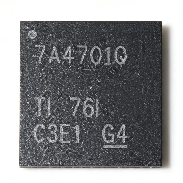
TPS7A4701QRGWRQ1 - 1A 35V Ultra-Low Noise LDO | TI Automotive
MPN: TPS7A4701QRGWRQ1 ✓ Active| Qty | Unit Price | Extended |
|---|---|---|
| 1 | $5.35 | $5.35 |
| 10 | $4.82 | $48.20 |
| 100 | $4.29 | $429.00 |
| 500 | $3.86 | $1,930.00 |
| 1,000 | $3.48 | $3,480.00 |
TPS7A4701QRGWRQ1 Overview
An LDO (low-dropout regulator) is a type of linear voltage regulator that maintains a stable output voltage even when the input is only slightly higher than the output. Within the power management IC hierarchy, the TPS7A47-Q1 sits at the precision post-regulation stage, typically cleaning up noisy switching-converter rails for sensitive analog loads.
Key features include 4.2 uVRMS output noise (20 Hz to 100 kHz), very high PSRR that suppresses upstream DC-DC ripple, an enable pin for power sequencing, thermal shutdown, and bipolar process technology optimized for RF and analog performance. According to TI datasheet for TPS7A47-Q1, the device is designed primarily for noise-critical RF signal chains.
Typical applications include automotive ADAS sensor power supplies, RF PLL/VCO rails, high-end audio DAC supplies, and precision data-converter reference rails. The 35V input tolerance supports automotive 12V and industrial 24V buses with load-dump headroom.
Design consideration: at large VIN-VOUT deltas and 1A load, power dissipation is significant - ensure adequate PCB copper area on the exposed pad. Prices as of 2026-08-29.
Drop-in alternatives for TPS7A4701QRGWRQ1 — same package, pin-to-pin compatible. Different-package parts requiring PCB rework are excluded.
Variants in this series
Same-series models that are drop-in compatible with TPS7A4701QRGWRQ1 (same form factor and footprint) — differing in Input Voltage Range, Output Noise, Output Type, Output Voltage Range.
Quick Comparison Tool — Select alternative parts for side-by-side comparison:
TPS7A4700QRGWRQ1
✓ In Stock
$3.65 / Unit
View Datasheet →TPS7A4701RGWR
✓ In Stock
$3.2467 / Unit
View Datasheet →TPS7A4701QRGWTQ1
📋 Reference alternative (not in catalog)
TPS7A4701-EP
📋 Reference alternative (not in catalog)
LT3045
📋 Reference alternative (not in catalog)
TPS7A4701QRGWRQ1 Maximum Ratings & Electrical Characteristics
| Output Type | Adjustable/Programmable |
| Output Voltage Range | 1.4 V to 34 V (adjustable), up to 20.5 V (PCB-programmable) |
| Maximum Output Current | 1 A |
| Input Voltage Range | Up to 35 V |
| Output Noise | 4.2 uVRMS (20 Hz to 100 kHz) |
| Regulator Topology | LDO (Low-Dropout Linear Regulator) |
| Number of Outputs | 1 |
| Polarity | Positive |
| Technology | Bipolar |
| Enable Pin | Yes |
| Protection Features | Thermal shutdown, current limit |
| Qualification | AEC-Q100 (Automotive) |
| Package | 20-VQFN (5x5 mm) with exposed pad |
| Mounting Type | Surface Mount |
| RoHS Status | Compliant |
| Packaging | Tape & Reel (T/R) |
TPS7A4701QRGWRQ1 Pin Configuration
| Pin 1-4 | IN — Input supply voltage (up to 35V) |
| Pin 5-8 | OUT — Regulated output voltage |
| Pin 9 | EN — Enable (active high) |
| Pin 10 | NR/SS — Noise reduction / soft-start capacitor |
| Pin 11 | FB — Feedback for adjustable output |
| Pin 12-15 | GND — Ground |
| Pin 16-20 | GND/Pad — Ground and exposed thermal pad |
| Pin PAD | PowerPAD — Exposed thermal pad, must be soldered to PCB ground |
Typical Applications
TPS7A4701QRGWRQ1 is suitable for 6 applications: Automotive ADAS Sensor Power, RF PLL/VCO Power Supply, Automotive Audio Amplifier Supply, Precision ADC/DAC Reference Rails, Industrial 24V Bus Post-Regulation, Automotive Body Electronics and Lighting.
Automotive ADAS Sensor Power
The TPS7A4701QRGWRQ1 suits ADAS radar and camera sensor rails with its 35V input tolerance and AEC-Q100 qualification. Its 4.2 uVRMS noise keeps radar LO chains and image-sensor analog rails clean, while the 1A output supports sensor SoC core supplies. Post-regulating a buck converter output with this LDO removes switching ripple via high PSRR, trading efficiency for noise-critical signal integrity in safety-rated systems.
Recommended
RF PLL/VCO Power Supply
RF synthesizers demand ultra-clean supplies because VCO pushing and phase-noise degradation track supply noise directly. The 4.2 uVRMS noise and high PSRR of the TPS7A4701QRGWRQ1 minimize spurs on PLL charge-pump and VCO tuning rails. Placing it after a switching preregulator yields a quiet 5V or 3.3V rail; the bipolar process maintains low noise across the audio-to-RF noise bandwidth cited in the TI datasheet.
Recommended
Automotive Audio Amplifier Supply
In infotainment and external amplifier designs, the TPS7A4701QRGWRQ1 provides a low-noise analog rail for DACs and preamplifiers. The 4.2 uVRMS specification keeps the noise floor far below the audible threshold, preserving dynamic range of 24-bit audio paths. The enable pin allows sequencing with the audio DSP supply, and AEC-Q100 qualification covers the harsh automotive cabin thermal environment.
Recommended
Precision ADC/DAC Reference Rails
High-resolution data converters need supply noise well below 1 LSB; the TPS7A4701QRGWRQ1 delivers with 4.2 uVRMS output noise. It post-regulates a buck-derived 5V rail down to a clean 3.3V AVDD at up to 1A. Its high PSRR rejects upstream converter ripple, avoiding clock spurs folding into the converter output band, making it suitable for test-measurement and industrial data acquisition front ends.
Recommended
Industrial 24V Bus Post-Regulation
The 35V maximum input accommodates industrial 24V rails with transient headroom, letting the TPS7A4701QRGWRQ1 serve as a final cleanup regulator for PLC analog modules, sensors, and instrumentation. Feeding it from a wide-VIN buck (e.g., 24V to 6V) then regulating to 5V achieves both efficiency and sub-5-uVRMS noise. Thermal design must account for the series dropout dissipation at 1A loads.
Recommended
Automotive Body Electronics and Lighting
The enable pin supports power sequencing and sleep-mode control in body control modules, while AEC-Q100 qualification meets automotive reliability requirements. The TPS7A4701QRGWRQ1 can supply low-noise analog sense rails and microcontroller analog supplies in lighting drivers and gateway modules. Its 1A capacity covers multiple low-power loads from one regulator, reducing BOM count versus distributed small LDOs.
Recommended
Recommended Products Summary
Engineering reference data for TPS7A4701QRGWRQ1 — comparison, design guidance, and compliance information.
Selection Guide
Comparison with Alternatives
| Parameter | This Product | TPS7A4700QRGWRQ1 | TPS7A4701RGWR | LT3045 |
|---|---|---|---|---|
| Package | VQFN-20 (5x5 mm) EP | VQFN-20 (5x5 mm) - same | VQFN-20 (5x5 mm) - same | LFCSP - pinout differs |
| Brand | Texas Instruments | Texas Instruments | Texas Instruments | Analog Devices |
| Output Current | 1 A | 1 A | 1 A | 0.5 A |
| Maximum Input Voltage | 35 V | 35 V | 36 V | 15 V |
| Output Noise | 4.2 uVRMS | 4.2 uVRMS | 4.17 uVRMS | 0.8 uVRMS |
| Output Voltage Range | 1.4 V to 34 V | 1.4 V to 34 V | 1.4 V to 34 V | 1.0 V to 15 V |
| AEC-Q100 Qualification | Yes (Q1) | Yes (Q1) | No | No |
| Enable Pin | Yes | No | Yes | Yes |
Key Differentiators
- Automotive AEC-Q100 qualification at 1A and 4.2 uVRMS noise (vs LT3045)
- Enable pin for power sequencing in the Q1 family (vs TPS7A4700QRGWRQ1)
- PCB-programmable fixed output option (vs TPS7A4701RGWR)
Design Notes
At VIN=13.5V (automotive rail), VOUT=5V, and 1A load, dissipation is approximately 8.5W. The VQFN-20 PowerPAD must be soldered to a substantial ground pour - TI layout guidelines recommend an array of thermal vias to inner ground layers. Above roughly 2-3W dissipation, evaluate junction temperature against the datasheet thermal resistance and consider reducing VIN-VOUT delta with a switching preregulator.
Place a 10uF ceramic input capacitor and 10uF output capacitor as close to the IN and OUT pins as possible. Connect the NR/SS capacitor (typically 10nF to 1uF) to reduce output noise below the standalone 4.2 uVRMS figure and to control soft-start ramp. Follow TI TPS7A47-Q1 datasheet layout section for FB divider placement to avoid noise pickup.
Do not exceed 35V input including automotive load-dump transients - use a TVS or upstream wide-VIN preregulator. Use 1%-tolerance FB divider resistors to hold output accuracy, and do not omit the NR/SS capacitor in noise-critical designs. When substituting TPS7A4700QRGWRQ1 (no EN pin), tie the enable net appropriately on the shared footprint.
Compliance Information
AEC-Q100 qualified per TI Q1 designation and DigiKey/Mouser listings. RoHS/lead-free per TI standard product page.







