Дискретные полупроводники
Подкатегории
Товары (1729)

SZNUP2105LT3G - Dual CAN Bus TVS ESD Protector | onsemi
The onsemi SZNUP2105LT3G is a dual-line CAN bus protector TVS diode providing bidirectional ESD and transient protection for both CAN data lines, with a 24V reverse standoff voltage, 44V maximum clamping voltage at 8A (8/20 us) peak pulse current, and 350W peak pulse power capability, housed in a compact 3-pin SOT-23 (TO-236) surface-mount package. A TVS (Transient Voltage Suppressor) diode is a semiconductor protection device that clamps fast overvoltage events such as electrostatic discharge (ESD), load dump, and inductive switching transients before they reach sensitive circuitry. In the power-protection hierarchy, TVS diodes sit at the board level, upstream protection layer, complementing fuses, varistors, and common-mode chokes in a complete electromagnetic-compatibility (EMC) front end. Key features include bidirectional protection on each of the two channels in a single package, a low 30pF line capacitance that preserves CAN FD and high-speed CAN signal integrity, and an automotive-grade SZ prefix indicating AEC-Q101 qualification for harsh environments. The 26.2V minimum breakdown voltage and 24V standoff rating give designers margin over the nominal 12V/24V vehicle rail transients seen on CAN_H and CAN_L. The device is specifically engineered for high-speed and fault-tolerant CAN networks per the onsemi datasheet, protecting the transceiver pins from ESD strikes and harmful transient voltage events. Its symmetrical bidirectional characteristic suits differential signaling, where both positive and negative overvoltages must be clamped relative to ground. Typical applications include automotive CAN_H/CAN_L line protection at the transceiver, industrial CANopen and DeviceNet nodes, 24V industrial bus protection, and general dual-line ESD protection for RS-485 style differential links. For design, place the SZNUP2105LT3G as close as possible to the connector side of the CAN transceiver, with a short, low-inductance ground return; excessive trace inductance degrades clamping performance during fast ESD edges. This page synthesizes distributor pricing, drop-in alternative comparisons, and practical design notes not found in the manufacturer datasheet alone.

SZNUP2124MXWTBG - 28V CAN/CAN-FD Dual TVS Protector | onsemi
The onsemi SZNUP2124MXWTBG is a dual bidirectional surge protection device (TVS diode) for CAN and CAN-FD data lines, rated for a 40V clamping voltage and 3A (8/20 us) peak pulse current, housed in an ultra-compact 3-pin XDFNW3 (1x1 mm) wettable-flank package. A TVS (transient voltage suppressor) diode is a circuit-protection semiconductor that clamps fast, high-energy voltage transients before they can damage sensitive transceiver ICs. Within the protection hierarchy, the SZNUP2124 sits at the board-level ESD/EMI layer of surge protection devices, complementing system-level protection such as varistors and upstream power supervision. Bidirectional devices like this one protect differential signaling lines where the signal swings both above and below ground, as in CAN and CAN-FD automotive buses. Key features include dual bidirectional channels in a single 1x1 mm footprint, Zener-based PN junction technology optimized for low dynamic resistance (Rdyn), a low turn-on voltage, and a wettable-flank package for reliable automated optical inspection (AOI). The device has been tested to EMI and ESD levels representative of ISO 7637-2 and ISO 7637-3 surge and transient events on road-vehicle power and data lines. Technically, the SZNUP2124 uses optimized Zener diode architecture that expands the active junction area, distributing transient energy and lowering dynamic resistance during an event. Lower Rdyn translates directly into a lower clamped voltage at the transceiver pins during a surge, which reduces stress on the CAN transceiver receiver front-end. The combination of low turn-on voltage and low dynamic resistance gives designers a low-cost option for improving system robustness without compromising signal integrity on 5 Mbps CAN-FD networks. Typical applications include CAN and CAN-FD bus line protection in automotive body, powertrain, and gateway ECUs, industrial CAN networks (DeviceNet, CANopen), and 12V/24V battery-system communication lines exposed to load-dump-like transients and ESD strikes at connectors. Design consideration: place the protector as close as possible to the connector or transceiver pins, and keep the clamp path (including ground return) short; parasitic series inductance dominates the actual clamped voltage during fast transients. This page synthesizes distributor pricing, drop-in variant options, and practical design notes not found in the manufacturer datasheet alone.
TA200616 - Phase Control SCR 1800A 2200V | Powerex
The Powerex TA200616 is a phase control SCR (silicon controlled rectifier) rated for 1600-1800 amperes average on-state current and blocking voltages spanning 100 to 2200 volts, intended for high-power AC line commutated conversion applications. A phase control SCR is a thyristor family device that switches from a blocking state to a conducting state when a small gate current pulse is applied at a controlled phase angle of the AC mains cycle. Within the power semiconductor hierarchy, it sits as a discrete thyristor, a sibling of the TRIAC and GTO, and a foundational building block of power conversion systems such as rectifiers, controlled bridges, and soft starters. Because conduction is latched, the device turns off only when the anode current falls below the holding threshold at each AC zero crossing, making it exceptionally rugged for line-frequency power control. The headline specifications of the TA200616, per the Powerex datasheet, are its very high average current class of 1600-1800 A and its wide repetitive peak voltage coverage from 100 V up to 2200 V. This voltage span allows one mechanical and thermal design to serve multiple line-voltage standards by selecting the appropriate voltage-code suffix. Devices in this class are typically supplied in press-pack (hockey-puck) housings with double-side cooling, which maximizes surge current capability, a critical parameter for failure-tolerant rectifier stacks and DC transmission valves. Phase control SCRs of this rating rely on a diffusion gate structure optimized for high di/dt immunity and low on-state voltage, which reduces conduction losses at thousands of amperes. Thermal design dominates: the heatsink, clamp force, and snubber network must be engineered around the surge (I2t) rating and gate trigger specifications published by the manufacturer. Typical applications include high-current DC power supplies, electrochemical rectifiers (chlorine, aluminum smelting), controlled DC motor drives, welding power sources, soft starters for large induction motors, and AC power controllers for furnace heating. When integrating this SCR, verify the exact voltage code of the ordered suffix against the datasheet, and apply RC snubbers sized to the manufacturer dv/dt limits to prevent unwanted triggering from line transients. This page consolidates verified distributor data, stock indications, and datasheet references for the TA200616, adding sourcing and application context not present in the manufacturer datasheet alone.

TJ30S06M3L(T6L1 - P-Ch 60V 30A 21.8mΩ DPAK+ MOSFET | Toshiba
The Toshiba TJ30S06M3L(T6L1 is a P-channel enhancement-mode power MOSFET built on Toshiba's U-MOS silicon process, rated for -60 V VDS, -30 A continuous drain current (Tc), and 68 W power dissipation, housed in a surface-mount DPAK+ (TO-252-3) package. According to the Toshiba datasheet, it delivers a typical RDS(ON) of 16.8 mΩ at VGS = -10 V and a maximum RDS(ON) of 21.8 mΩ, with a gate threshold of -3.0 V (VDS = -1 mA) and maximum leakage IDSS of -10 µA at VDS = -60 V. The (T6L1,NQ suffix denotes the tape-and-reel packaging variant aimed at high-volume automotive and industrial assembly lines. A P-channel MOSFET is a voltage-controlled transistor in which a negative gate-source voltage creates a conductive P-type channel between source and drain. Unlike N-channel MOSFETs, P-channel devices can be placed on the high-side of a load without a charge pump, simplifying reverse-polarity protection, load switching, and high-side drive circuits. P-channel MOSFETs sit within the broader power-MOSFET taxonomy: power MOSFET > MOSFET > field-effect transistor > discrete semiconductor, making them a foundational building block in modern switching power conversion. Key differentiating features of the TJ30S06M3L(T6L1 include AEC-Q101 automotive qualification, an ultra-low RDS(ON) of 16.8 mΩ typical that minimizes conduction losses, and a low gate charge suitable for high-frequency switching. The -3.0 V typical Vth allows direct CMOS/TTL logic-level driving without a gate driver in many applications. Built on Toshiba's U-MOS process, the cell pitch is optimized for the 60 V breakdown class to balance RDS(on), switching speed, and avalanche ruggedness. The DPAK+ package offers an exposed thermal pad and a tab that doubles as the drain terminal, achieving a junction-to-case thermal resistance (RθJC) suitable for 68 W continuous dissipation with adequate PCB copper. Typical applications include automotive motor drivers (power seats, window lifts, fuel pumps, fans), DC-DC converters (buck and buck-boost topologies), switching voltage regulators, reverse-battery protection circuits, and high-side load switches in industrial PLCs and battery management systems. The 60 V drain rating provides comfortable headroom for 12 V and 24 V automotive bus transients while supporting 48 V mild-hybrid loads in newer systems. When designing with this MOSFET, verify that VGS does not exceed the ±20 V absolute maximum rating, and place the gate-source pull-down resistor (typically 10 kΩ-100 kΩ) directly across the gate-source pins to prevent accidental turn-on from leakage or dv/dt-induced Miller coupling. Use a low-impedance gate-drive path with appropriate series resistance to limit ringing and overshoot in high-di/dt switching applications. This page synthesizes distributor stock data, drop-in alternatives from verified cross-references, and practical PCB layout notes not collected in the manufacturer datasheet, giving engineers a faster path to qualified sourcing and replacement decisions for the TJ30S06M3L(T6L1.
TJ50S06M3L - P-Ch 60V 50A 10.3mΩ U-MOSVI MOSFET | Toshiba
The Toshiba TJ50S06M3L is a P-channel enhancement-mode power MOSFET built on Toshiba's latest-generation U-MOSVI silicon process, rated for -60 V VDS, -50 A continuous drain current (Tc), and a typical RDS(on) of 10.3 mΩ at VGS = -10 V, housed in a surface-mount DPAK+ (TO-252-3) package. Its 90 W (TC) power dissipation and 13.8 mΩ maximum on-resistance position it as a high-current, low-loss switching element for automotive motor drivers, DC-DC converters, and switching voltage regulators. The device is qualified to AEC-Q101 for automotive-grade reliability, and the gate is rated for +10 V / -20 V VGS with a low threshold suitable for direct gate-drive from logic-level or standard MOSFET drivers. A P-channel MOSFET (P-ch) is a voltage-controlled field-effect transistor in which the channel region between source and drain is formed by inversion of n-type silicon under a negative gate-source voltage. Unlike N-channel MOSFETs (which require a gate drive above the source, often necessitating a charge pump or bootstrap), P-channel MOSFETs simplify high-side switching because their source sits at the load supply rail and a simple pull-down (or logic-low) gate signal turns them on. P-ch devices are commonly used in load switching, reverse-battery protection, motor reverse-braking, and high-side half-bridge or synchronous-rectifier positions where ease of drive outweighs the on-resistance penalty inherent to P-channel silicon. Key differentiating features of the TJ50S06M3L include Toshiba's U-MOSVI cell structure, which optimizes the trade-off between RDS(on) × Qg figure-of-merit and avalanche ruggedness. The 13.8 mΩ max RDS(on) at VGS = -10 V delivers low conduction loss in 30-40 A continuous-load paths, while the small TO-252-3 footprint allows direct substitution for legacy D-PAK footprints. The part also integrates a body-drain diode for synchronous-rectifier and freewheeling applications. Typical applications span automotive electronic power steering (EPS), brushless DC (BLDC) motor drivers for HVAC blowers and water pumps, 12 V bidirectional DC-DC converters in mild-hybrid systems, load switches and high-side OR-ing for redundant supplies, and switching voltage regulators. It is also a strong candidate for industrial-aggressive robotics, e-bike controllers, and battery management protection FET positions. When designing with this device, ensure the gate-source rating of +/-20 V is never exceeded and that adequate thermal copper (>=1 sq. inch of 2 oz pour) is provided under the DPAK+ tab. P-channel parts dissipate heat through the drain tab; do not rely on plastic-only thermal dissipation. This page synthesizes distributor pricing, drop-in alternatives, and practical design notes not found in the manufacturer datasheet.
TJ60S06M3L - P-Ch 60V 60A 11.2mΩ U-MOSVI MOSFET | Toshiba
The Toshiba TJ60S06M3L is a P-channel enhancement-mode power MOSFET built on the U-MOSVI silicon process, rated for -60 V VDS, -60 A continuous drain current, and a maximum power dissipation of 100 W (Tc). It is housed in a surface-mount DPAK+ (TO-252-3 lead-form) package with a typical on-resistance of 11.2 mΩ at VGS = -10 V, making it suitable for high-current switching applications. A Power MOSFET (Metal-Oxide-Semiconductor Field-Effect Transistor) is a voltage-controlled three-terminal semiconductor used for switching and amplifying signals in power electronics. P-channel MOSFETs specifically conduct when a negative gate-source voltage is applied, making them ideal for high-side switching where one terminal sits at the load supply. The TJ60S06M3L belongs to the U-MOSVI generation, which Toshiba's datasheet describes as offering low on-resistance, low leakage, and a -3.0 V enhancement-mode threshold for low-voltage gate drive compatibility. Key electrical characteristics include RDS(ON) of 11.2 mΩ (typ.) at VGS = -10 V, a low drain leakage IDSS of -10 µA (max) at VDS = -40 V, and an enhancement-mode threshold Vth of -3.0 V measured at VDS = -1 mA. The 7760 pF typical input capacitance (consistent with the Mouser datasheet snippet) reflects a die optimized for low gate charge rather than ultra-fast switching. The DPAK+ package provides a tab that acts as the drain connection and the primary thermal path, supporting sustained 60 A operation with proper heatsinking. Architecturally, this part uses Toshiba's U-MOSVI trench cell structure, which reduces cell pitch to lower on-resistance per unit area while keeping the Miller plateau modest. The result is a P-channel die that competes with similarly rated N-channel parts in 60 V class, but in a package commonly chosen for high-side load switching. The automotive-grade LJ suffix (AEC-Q101 qualified) is also available, designated TJ60S06M3L,LXHQ. Typical applications include high-side load switches in automotive ECUs, motor driver H-bridges, DC-DC converter high-side switches, and switching voltage regulators. Its low RDS(ON) reduces conduction loss in continuous-current paths such as reverse-battery protection circuits. Design considerations include keeping the gate-source loop area small to minimize ringing at turn-on, and ensuring the source-pin PCB copper area is sufficient to carry the full 60 A without excessive voltage drop.
TJ60S06M3L(T6L1,NQ - 60V 60A P-Ch MOSFET DPAK+ | Toshiba
The Toshiba TJ60S06M3L(T6L1,NQ is a P-channel silicon power MOSFET rated at -60 V VDS, -60 A continuous drain current, and 100 W power dissipation, housed in a surface-mount DPAK+ (TO-252-3) package. Built on Toshiba's U-MOS process, it delivers a typical on-resistance of 11.2 mOhm at VGS = -10 V and a typical threshold voltage of -3.0 V, achieving a figure of merit that suits high-current switching applications. The device is qualified to AEC-Q101 for automotive reliability. A P-channel MOSFET (P-FET) is a type of metal-oxide-semiconductor field-effect transistor in which the body-source p-n junction is reversed-biased and majority-carrier conduction is by holes rather than electrons. P-channel MOSFETs belong to the broader category of power MOSFETs (MOSFET -> discrete semiconductor -> power transistor), and they occupy a unique role in high-side switching because their source sits at the load supply rail, simplifying gate drive when the load must be switched to ground. P-FETs are commonly used as reverse-polarity protection devices, high-side load switches, and synchronous-rectifier replacements in low-voltage buck converters. Key features of the TJ60S06M3L include a maximum drain-source on-resistance RDS(ON) of 14.5 mOhm at VGS = -10 V, a low input capacitance Ciss of 7760 pF that keeps gate-drive losses manageable, and an enhancement-mode threshold that allows direct logic-level gate drive from -3.3 V or -5 V microcontrollers. The DPAK+ tab provides a low-thermal-resistance path (junction-to-case) suitable for continuous high-current operation with modest PCB copper area. The architecture uses Toshiba's latest-generation U-MOS trench cell, which lowers specific on-resistance versus older planar P-FET generations, and integrated gate-protection circuitry to limit avalanche energy. Compared with a mechanical relay, the MOSFET offers silent, fast (<50 ns half-controlled) switching and zero contact bounce, while compared with a PNP bipolar transistor it eliminates base-drive current and the saturation-voltage knee. Typical applications for this part include automotive reverse-battery protection, DC-DC converter high-side switches, motor-driver H-bridges (low-side or high-side position), and switching voltage regulators in industrial power systems. Because of its 60 V rating it can replace mechanical relays in 24 V and 48 V automotive and industrial buses. Design tip: when using the TJ60S06M3L as a reverse-polarity protection FET, ensure that the gate is pulled to ground through a resistor when the system is off; floating gates can leave the FET in an undefined state and create leakage paths. Also note that the AEC-Q101 grade makes this part suitable for under-hood automotive designs where ambient temperatures can reach 125 C.
TJ60S06M3L(T6L1,NQ - P-Ch -60V -60A 11.2mOhm DPAK+ MOSFET | Toshiba
The Toshiba TJ60S06M3L(T6L1,NQ is a P-channel silicon power MOSFET built on Toshiba's U-MOS process, rated for -60 V VDS, -60 A continuous drain current (TC), and a maximum power dissipation of 100 W. Housed in a surface-mount DPAK+ (TO-252 with extended leads) package, it delivers an ultra-low on-resistance of 0.0112 ohm at VGS = -10 V, with an input capacitance (Ciss) of 7760 pF. A P-channel MOSFET is a voltage-controlled field-effect transistor in which the conductive channel is formed by holes rather than electrons. Because P-channel devices turn on with a negative gate-source voltage, they simplify high-side switching in circuits where the load is tied to ground - no charge pump or bootstrap network is needed to drive the gate. P-channel MOSFETs are typically placed in the power-MOSFET hierarchy under 'P-channel -> MOSFET -> power MOSFET -> discrete semiconductor' and are widely used as reverse-polarity protection, high-side load switches, and synchronous-rectifier complements in DC-DC converters. Key features of the TJ60S06M3L include the very low 11.2 milliohm Rds(on) at full gate drive, the -60 V drain rating that provides substantial avalanche headroom for 12 V / 24 V automotive buses, and an industry-standard DPAK+ footprint that allows direct PCB mounting with a thermal pad for low thermal resistance. The part is qualified for automotive motor drivers, DC-DC converters, and switching voltage regulators per Toshiba's product family positioning. Technically, the device uses Toshiba's latest-generation U-MOS trench cell structure to achieve a per-cell figure-of-merit (FOM = Rds(on) x Qg) optimized for switching loss reduction. This makes it particularly suitable for hard-switched applications up to several hundred kHz where switching losses dominate conduction losses. The P-channel polarity allows direct logic-level driving from standard microcontrollers without additional gate-driver circuitry. Typical applications include automotive ECU load switching, motor-driver H-bridge high-side switches, battery management system (BMS) reverse-polarity protection, synchronous-rectifier secondary-side switches in isolated DC-DC converters, and high-current load management in industrial 24 V systems. The DPAK+ package's exposed thermal pad allows direct PCB heatsinking. When designing with this device, mind the gate-source voltage rating of +10 V / -20 V - the absolute maximum must not be exceeded even during transients. Use a gate-source resistor (typically 10 kohm) to prevent inadvertent turn-on from Miller-coupling during drain-voltage transients. Verify continuous drain current against your thermal envelope using the SOA curve from the manufacturer datasheet. This page synthesizes distributor pricing, drop-in alternatives, and practical design notes not found in the manufacturer datasheet alone, providing a single reference for sourcing and second-sourcing the TJ60S06M3L(T6L1,NQ.

TL431AIDBVR - 2.495V-36V Adjustable Shunt Reference, 1% | Texas Instruments
The Texas Instruments TL431AIDBVR is a precision adjustable shunt voltage reference that delivers a programmable output from 2.495V to 36V with a 1% initial tolerance (A grade) in a 5-pin SOT-23 (DBV) package. It provides up to 100 mA of cathode current with low dynamic impedance of 0.2 ohm typical, making it functionally equivalent to a non-isolated Zener diode but with tighter tolerance and adjustable setpoint. A shunt voltage reference is a two-terminal (plus reference pin) device that maintains a constant voltage across its terminals by shunting excess current to ground, analogous to a Zener diode but with programmable breakdown voltage. Shunt references form a sub-category of voltage references within the broader voltage regulator hierarchy (voltage reference -> shunt regulator -> analog reference circuit -> signal chain IC), and they are foundational building blocks for power supply feedback, ADC reference rails, comparator thresholds, and error amplifiers in isolated and non-isolated converter topologies. Key features of the TL431AIDBVR include a 2.495V reference voltage (Vref) with 1% initial accuracy at 25C, an operating cathode current range of 1 mA to 100 mA, typical dynamic impedance of 0.2 ohm at 1 kHz, and an operating temperature range of -40C to +85C. The SOT-23-5 surface-mount package offers a compact footprint while exposing the reference, anode, and cathode pins in a standardized layout used industry-wide across second-source vendors. The TL431 architecture uses a buried-Zener bandgap reference cell feeding an on-chip op-amp that drives a pass transistor, producing a sharp knee in the I-V curve and excellent thermal stability. According to the manufacturer datasheet, the device exhibits typical output impedance of 0.2 ohm over 1 kHz and a wideband noise figure suitable for switch-mode power supply feedback loops and audio threshold detection. Typical applications include SMPS secondary-side regulation, isolated flyback error amplifier reference, adjustable Zener replacement, voltage monitoring and reset circuits, and precision current limiting. The SOT-23-5 form factor is well suited for high-density DC-DC converter boards and compact adapter designs. When designing with the TL431AIDBVR, ensure the cathode current stays between 1 mA and 100 mA across all load and line conditions, including start-up transients. Place the device close to the opto-coupler or error-amplifier input to minimize loop-area noise pickup, and use a bypass capacitor on the reference pin if the application requires low AC noise. This page synthesizes distributor pricing, drop-in alternatives, and practical design notes not found in the manufacturer datasheet alone.
TL431AIDBVRG4 - 2.495V Adjustable Shunt Reference | Texas Instruments
The Texas Instruments TL431AIDBVRG4 is a precision programmable shunt voltage reference IC with an adjustable output of 2.495 V to 36 V, ±1% initial accuracy, and 100 mA cathode current capability, housed in a 5-pin SOT-23 (DBV) package. It belongs to the TL431 family of three-terminal adjustable shunt regulators specified for operation from -40°C to 85°C, with the G4 suffix marking the lead-free, RoHS-compliant, tape-and-reel packaging option. A shunt voltage reference is a two-terminal (or three-terminal with adjustment) device that maintains a constant voltage across its terminals by sinking varying amounts of current through a parallel load. Shunt references sit at the same hierarchy level as series (bandgap) references, but are wired in parallel with the load rather than in series — making them functionally closer to a Zener diode than to a LDO regulator. The TL431 family implements an adjustable bandgap core with an on-chip op-amp and reference network, allowing the user to set the output via an external resistor divider. Key features include a typical output impedance of 0.2 Ω at low frequencies, a low output noise of approximately 0.2 µV_RMS across the audio band, and a temperature coefficient of 109 ppm/°C (max). The device sinks from 1 mA (minimum cathode current for regulation) up to 100 mA continuously, with absolute-maximum cathode voltage of 37 V. The SOT-23-5 footprint offers a compact land pattern of approximately 2.9 mm × 1.6 mm, suiting it to high-density switching supply and isolated feedback designs. The TL431 architecture pairs a precision bandgap reference with a transconductance error amplifier driving an open-collector pass transistor. When the divided output drops below the internal 2.495 V bandgap, the amplifier reduces cathode conduction, raising V_OUT; when it rises above, conduction increases, clamping V_OUT. This feedback loop yields tight line and load regulation in closed-loop SMPS optocoupler and primary-side feedback circuits. Typical applications include isolated DC-DC converter secondary-side regulation, switch-mode power supply (SMPS) feedback loops, adjustable Zener replacement, voltage monitoring, and precision comparator thresholds. Its wide cathode voltage range makes it ideal for 3.3 V, 5 V, 12 V, and 24 V rails. The combination of small SOT-23 footprint and high accuracy is particularly valuable in industrial PSU designs with tight PCB constraints. When designing with this part, ensure the cathode current stays between 1 mA and 100 mA under all load and line conditions. Add a 0.1 µF bypass capacitor close to the cathode pin when the device operates in fast-loop SMPS feedback paths to suppress transient oscillation. Choose resistors in the divider for low standby current, and ensure the divider current is at least 100× the TL431 reference bias current for accuracy. This page synthesizes distributor pricing, drop-in alternatives, and practical design notes not found in the manufacturer datasheet.
TL431ASA-7 - Adjustable Shunt Regulator 36V 1% SOT-23-3 | Diodes Inc.
The Diodes Incorporated TL431ASA-7 is an adjustable precision shunt voltage reference regulator with a 2.495V bandgap reference, ±1% initial tolerance, adjustable output range up to 36V, and 100mA cathode current capability in a 3-pin SOT-23 (SOT-23-3) surface-mount package. An adjustable shunt regulator is a three-terminal voltage reference device that maintains a precise voltage across its cathode and anode terminals by shunting excess current, controlled by an external resistor divider connected to the reference pin. In the power-management hierarchy, it sits below switching regulators and linear regulators as the precision building block used to set feedback thresholds, and it is one of the most widely used reference ICs in the industry, with the TL431 function being a de-facto industry standard footprint. Key features of the TL431ASA-7 include the ±1% initial reference accuracy of the A-grade die, a temperature-compensated bandgap reference, and a low dynamic output impedance. According to the Diodes Incorporated datasheet, the TL431 series has the same electrical specifications as the industry-standard '431 and is offered in A (1%) and B (0.5%) accuracy grades. The device operates as either a shunt regulator or an open-collector comparator with a 2.495V threshold, giving engineers two functions in one package. Technically, the part uses an internal bandgap reference and an output amplifier driving a shunt transistor. When the reference pin voltage exceeds 2.495V, the device sinks current from cathode to anode, holding the reference pin at 2.495V. With two external resistors the output is programmable from 2.495V up to 36V. The primary use case is as the error amplifier and reference in the feedback loop of flyback and buck switching power supplies, optocoupler-coupled feedback networks, and precision comparators. Typical applications include SMPS feedback regulation, battery chargers, adjustable zener replacement, voltage monitoring thresholds, and constant-current source circuits. Its low cost and small SOT-23-3 footprint make it suitable for both industrial and consumer designs. A key design consideration is ensuring the cathode current stays above the minimum regulation level (typically ~1mA region) across load and temperature for guaranteed regulation, and choosing divider resistor values that balance accuracy against quiescent loading. This page adds information gain beyond the datasheet by combining distributor pricing tiers, cross-brand drop-in alternatives, comparison tables, and practical design notes in one place.
TL431BFDT - Adjustable Shunt Regulator 2.495-36V SOT-23 | Nexperia
The Nexperia TL431BFDT is a three-terminal adjustable precision shunt voltage regulator with a reference voltage of 2.495 V, an adjustable output range from 2.495 V to 36 V set by two external resistors, and a cathode current capability up to 100 mA, housed in a 3-pin SOT-23 (TO-236AB) surface-mount package. A shunt regulator (also called a shunt voltage reference) is a type of voltage regulator that maintains a set voltage across its terminals by sinking or sourcing current in parallel with the load. Unlike a series regulator, the shunt topology sits across the supply path and absorbs surplus current, making it the workhorse of the voltage reference family within power management and discrete semiconductor hierarchies. The TL431 is the industry-standard part of this class, widely used in isolated and non-isolated power supplies. The TL431BFDT offers a tight B-grade reference tolerance of +/-0.5% at 25 C, an operating temperature range of -40 C to +125 C (Q-grade qualification per Nexperia automotive designation), and enhanced stability with a very low minimum load capacitance requirement in the FDT variant family. According to the Nexperia product page, the family covers reference tolerances from 2.0% down to 0.5% and temperature ranges up to 125 C, with AEC-Q100 qualification noted for automotive use. Architecturally, the device integrates a 2.495 V bandgap reference, an error amplifier, and an open-collector output transistor. When the voltage at the REF pin exceeds the internal reference, the output transistor conducts cathode current, regulating the cathode voltage in closed-loop configurations such as optocoupler feedback in flyback converters. Typical applications include secondary-side feedback regulation in AC-DC adapters and flyback SMPS, adjustable voltage references in battery chargers, overvoltage protection crowbars, and setpoint generation in LED drivers. Design-wise, provide a minimum cathode bias current (about 1 mA) for regulation and add a small compensation capacitor at REF for loop stability in optocoupler feedback paths. This page synthesizes verified distributor data, drop-in alternatives, pricing, and practical design notes not found in the manufacturer datasheet.
TL431CDBZR - Adjustable 2.495V Shunt Reference 100mA SOT-23-3 | TI
The Texas Instruments TL431CDBZR is a three-terminal adjustable precision shunt voltage reference IC with a programmable output range of 2.495 V to 36 V, up to 100 mA sink current capability, and ±2.2% initial reference tolerance, housed in a 3-pin SOT-23 (DBZ) surface-mount package. An adjustable shunt regulator (also called a programmable shunt reference) is a type of voltage reference IC that regulates voltage by sinking current from a supply rail through its cathode when the reference pin senses a voltage above an internal bandgap threshold. In the power-management hierarchy, it sits between a fixed zener diode and a full linear regulator: more precise and temperature-stable than a zener, yet far cheaper and simpler than an LDO. Because the output is set by just two external resistors, the shunt reference family is a fundamental building block in analog circuit design. Key features include a wide adjustable output range set by two external resistors, approximately 2.495 V internal reference with 2.2% (standard C grade) initial tolerance, 0.2 ohm to 0.5 ohm order typical dynamic output impedance, and a maximum cathode current of 100 mA. The C-grade device is specified over the 0 C to 70 C commercial temperature range, and its low minimum cathode current of roughly 1 mA allows operation in low-power systems. Technically, the TL431 combines an internal 2.495 V bandgap reference with an operational amplifier and an open-collector output transistor. When the REF pin exceeds the internal threshold, the output transistor conducts and sinks current from cathode to anode, forming the basis of error-amplifier action in isolated flyback and forward power supplies, where the TL431 is frequently paired with an optocoupler such as the PC817 for secondary-side feedback. Typical applications include secondary-side voltage regulation and feedback in AC-DC and DC-DC switch-mode power supplies, adjustable zener replacement and overvoltage crowbar sensing, battery charger voltage monitoring, and precision threshold comparators in industrial instrumentation. A critical design consideration is temperature drift: the C grade (2.2% at 25 C) drifts more than the A or B grades over temperature, so precision systems should select TL431ACDBZR or TL431BDBZR instead. Always provide at least the minimum cathode current for regulation. This page adds distributor pricing, drop-in alternatives, and practical design notes not found in the manufacturer datasheet.

TL431ILPR - Adjustable 2.495V Shunt Reference | TI
The Texas Instruments TL431ILPR is a three-terminal adjustable precision shunt regulator with a 2.495V reference voltage, up to 100mA sink-current capability, and cathode voltage operation to 36V, housed in a 3-pin TO-92 (LP) through-hole package supplied on tape and reel. According to TI, the standard grade TL431I offers an initial reference tolerance of 2% at 25C. An adjustable shunt regulator is a type of voltage reference IC that maintains a programmed voltage across its cathode-anode terminals by sinking current when the sense voltage at its reference pin exceeds an internal bandgap threshold. Within the power-management hierarchy it sits below linear regulators as a precision reference element, and it is widely used as the feedback error amplifier inside isolated and non-isolated switching power supplies. Key features of the TL431ILPR include a programmable output voltage set anywhere from Vref (approximately 2.5V) to 36V using just two external resistors, a sharp low-dynamic-output-impedance characteristic, low output noise, and a typical temperature coefficient in the low ppm/C range across the specified -40C to +85C industrial operating range. Its 1mA to 100mA sink-current range gives designers wide loop-gain control in optocoupler feedback networks. Technically, the TL431 combines an internal 2.495V bandgap reference with an open-collector-style error amplifier driving the cathode output. Because the reference input draws only about 2uA typical, high-impedance divider networks are practical. The device is stable with appropriate capacitive loading per the stability boundary in the manufacturer datasheet, and it is specified for thermal stability over automotive, commercial, and military temperature grades across the family. Typical applications include secondary-side voltage regulation in flyback and forward AC-DC power supplies, adjustable zener replacement in overvoltage protection Crowbar circuits, precision current-source and current-limiter biasing, and set-point generation in battery chargers. Its three-pin simplicity and low cost make it the industry default feedback element driving optocoupler LEDs in isolated converters. Design-wise, keep the cathode current above the 1mA minimum for regulation and respect the datasheet stability criteria when adding decoupling capacitance at the cathode node; the compensation capacitor interacts with the equivalent series resistance in ways that can destabilize the loop. This page synthesizes distributor pricing, drop-in cross-brand alternatives, pinout detail, and practical design notes not consolidated in the manufacturer datasheet.

TLP183(GB-TPL,E - 3750Vrms Phototransistor Optocoupler SO6
The Toshiba TLP183(GB-TPL,E is a 4-pin SO6 phototransistor optocoupler providing 3750 Vrms isolation voltage, DC input, and a current transfer ratio (CTR) rank of GB (100% to 300% at IF=5 mA). It is housed in a miniature 6-SOP surface-mount package (Toshiba designation 4-pin SO6) that combines a high-emission infrared LED with a phototransistor detector optically coupled in a plastic DIP-style body. A phototransistor optocoupler is a galvanic isolation device that transfers an electrical signal between two circuits using light, blocking high voltages and transient surges while transmitting the analog or digital signal at the speed of the photodetector. Within the broader component taxonomy, the TLP183 belongs to optoisolators > optocouplers > solid-state relays > isolators > discrete semiconductors, with the phototransistor output placing it in the same family as the Toshiba TLP181, TLP185 and TLP184 series. Key features include 3750 Vrms minimum isolation voltage, 50 mA maximum forward current, 80 V collector-emitter breakdown voltage, 50 mA collector current, and an operating temperature range of -55C to +110C. The GB CTR rank provides 100% to 300% typical transfer ratio at IF=5 mA and VCE=5 V, which is well suited to digital signal isolation in PLCs and communication interfaces. A GaAs infrared LED emitter delivers fast switching with rise/fall times measured in microseconds. The TLP183 employs a high-isolation optically-coupled architecture: the input-side GaAs LED converts the input current into modulated infrared light that crosses an internal transparent isolation barrier, after which a silicon phototransistor converts the light back into a current at the output side. The result is complete electrical isolation between input and output while preserving the timing and amplitude characteristics of the original signal. Typical applications include PLC digital input/output isolation, communication interface isolation (RS-232, RS-485 line-side isolation), power supply feedback loops, and AC mains detection circuits where 3750 Vrms isolation is required by safety standards. The wide -55C to +110C temperature range also supports industrial and consumer-grade equipment. When designing with the TLP183, ensure that the bias resistor on the LED side limits the forward current to within 50 mA DC, and that the collector pull-up resistor is sized according to the desired switching speed and the chosen CTR rank. Proper creepage and clearance around the SO6 body must be maintained to preserve the 3750 Vrms isolation rating in end-equipment safety certification. This page synthesizes distributor pricing, drop-in same-brand alternatives, parametric comparison and practical design notes not found in the standalone Toshiba datasheet.
TLV431IDBVR - 1.5% 6V Adj Shunt Reference | Texas Instruments
The Texas Instruments TLV431IDBVR is a low-voltage three-terminal adjustable precision shunt regulator providing a 1.24 V reference with ±1.5% initial accuracy and 15 mA maximum cathode current, housed in a 5-pin SOT-23 (DBV) package. Output voltage is programmable from VREF (1.24 V) to 6 V through two external resistors, enabling flexible rail design from sub-1.5 V point-of-load references up to small analog and digital supplies. The low minimum cathode current of 80 µA (typical) makes the part well suited to low-power and always-on circuits. A shunt voltage reference such as the TLV431 is functionally a two-terminal analog building block - when biased with a resistor from a higher supply, it conducts current through its cathode-to-anode path to hold its reference pin at the programmed voltage. As a category, voltage references sit alongside linear regulators, supervisors, and ADC/DAC references inside the power management IC hierarchy, and behave as programmable Zener diodes with much tighter tolerance and lower dynamic impedance than discrete components. They are the building blocks of closed-loop SMPS feedback, precision comparators, and adjustable linear regulators. Key features of the TLV431 family include 1.24 V typical reference with ±1.5% tolerance (the tighter TLV431A grade specifies ±1%), a wide programmable output range of VREF to 6 V, 80 µA typical minimum cathode current, low output impedance of 0.25 Ω typical, and operation across -40 °C to +85 °C industrial/commercial temperatures. The 5-pin SOT-23 (DBV) footprint enables drop-in replacement among TLV431 grades and competitor parts in the same pin-out. Architecturally, the TLV431 uses a bandgap-derived 1.24 V reference buffer, an internal error amplifier that compares the reference pin to VREF, and a pass transistor that sinks current to regulate the output. The wide cathode operating range and low dynamic impedance allow the regulator to maintain tight output regulation across load and supply variations typical of switching-supply feedback loops. Typical applications include switching-supply secondary-side feedback, adjustable linear regulator references, isolated point-of-load rails, precision comparator thresholds, and ADC/DAC reference circuits. Engineers may also use the TLV431 as a low-cost, low-power replacement for a TL431 where lower minimum cathode current and a smaller SOT-23-5 package are required. When designing with the TLV431, size the cathode bias resistor to keep the device above its minimum operating current (80 µA typical) under worst-case load, and add a capacitor on the reference pin if the application demands transient stability. Because the part ships in the small SOT-23-5 outline, expect to follow standard SMD PCB layout practices - minimize reference-pin leakage and route the cathode trace away from switching nodes. This page synthesizes distributor pricing, drop-in alternatives, and practical design notes not found on the manufacturer datasheet, giving engineers a single reference for sourcing, second-sourcing, and properly biasing the TLV431IDBVR in low-voltage reference designs.
TPD1E10B06DPYR - Single-Channel ESD TVS Diode, ±30kV | TI
The Texas Instruments TPD1E10B06DPYR is a single-channel ESD protection TVS diode rated for ±30kV contact and ±30kV IEC air-gap ESD discharge in a compact 2-pin X1SON (DPY) package measuring approximately 1.0 x 0.6 mm. It provides a 14V working voltage rating with 5A peak pulse current (8/20 µs waveform) and integrated back-to-back TVS diodes for bipolar or bidirectional signal support, making it suitable for both positive- and negative-going transients on a single line. What is a TVS diode? A TVS (transient voltage suppressor) diode is a clamping semiconductor that diverts ESD and surge energy away from sensitive downstream ICs. Within the protection hierarchy (TVS -> protection diode -> discrete semiconductor -> electronic component), TVS arrays sit closest to external connectors, where they shunt fast transients (ns-scale ESD, µs-scale surge) before they reach ASICs, MCUs, or analog front-ends. The TPD1E10B06 family uses a back-to-back configuration to handle bipolar signals. Key specifications include 12pF (typical, per DigiKey listing; datasheet lists 10pF IO capacitance typical and 12pF line capacitance) line capacitance, 0.37 Ω dynamic resistance (R_DYNAMIC), and ±6V minimum DC breakdown voltage. The 0402-class footprint frees PCB real estate for high-density mobile and wearable designs where every square millimeter matters. The device is rated for ultra-low leakage current, minimizing quiescent loss on protected lines. Architecturally, the TPD1E10B06 uses a silicon TVS structure with back-to-back Zener diodes, achieving system-level IEC 61000-4-2 ESD immunity. Its low capacitance suits data lines like USB VBUS/ID, audio (microphone, headphone, speakerphone), SD card interfaces, keypads, and GPIO. The bidirectional capability removes the need for two unidirectional TVS in many use cases, halving the BOM on differential or AC-coupled lines. Typical applications include protection for audio lines (microphone, earphone, speakerphone), SD card interfaces, keypad buttons, USB port VBUS/ID pins, and general-purpose GPIO. End-equipment targets are portable devices, wearables, set-top boxes, electronic point-of-sale terminals, and appliances. The low 12pF capacitance preserves signal integrity on high-speed interfaces. Design tip: place the TPD1E10B06DPYR as close as possible to the external connector with a short, low-inductance ground return. Use a dedicated TVS ground via directly to the chassis/ground plane to maximize the IEC 61000-4-2 discharge current path and avoid coupling noise into adjacent signal traces. This component is also available in a larger SOD-523 (DPYT) variant on the same datasheet for layouts needing a different footprint.
TPD2E001DRLR - 2Ch ESD Protection Array SOT-5 | Texas Instruments
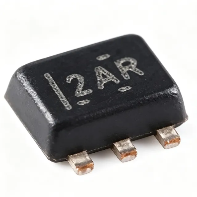
The Texas Instruments TPD2E001DRLR is a 2-channel Transient Voltage Suppressor (TVS) based Electrostatic Discharge (ESD) protection diode array rated to handle ESD strikes up to ±15 kV (HBM) and ±8 kV (IEC 61000-4-2 contact) with a typical channel capacitance of 1.5 pF, housed in a 5-pin SOT (DRL) package for space-constrained high-speed data lines. An ESD protection diode array is a circuit-protection component that shunts transient voltage events to ground, protecting sensitive downstream ICs from electrostatic discharge. In the electronics taxonomy, TVS diode arrays sit under discrete semiconductors > diodes > TVS protection devices, where they form the lowest-level shield in a layered PCB protection strategy (typically used alongside common-mode chokes, PTC fuses, and bulk TVS). Because high-speed interfaces carry multi-Gbps signals, the protection device must add minimal parasitic capacitance so the signal eye diagram remains compliant with USB, HDMI, or LVDS masks. Key features include a working range up to 5.5 V, a typical clamping voltage of 16 V, and a dynamic resistance of 1.2 Ω. Two TVS channels are integrated into one 5-pin SOT package, allowing protection of a differential pair (D+, D-) or two single-ended lines from a single component. The low 1.5 pF line capacitance minimizes insertion loss on USB 2.0, LVDS, HDMI, and Ethernet signal paths, and the device is qualified to IEC 61000-4-2 Level 4 for air and contact discharge. Technically, the TPD2E001DRLR uses a steering-diode + Zener-clamp TVS architecture that biases through an optional VCC pin. When VCC is tied to the protected supply rail, the clamping voltage is tightened; when left floating, the device still clamps but with slightly higher residual voltage. The 1.2 Ω dynamic resistance ensures that even at 8 kV contact discharge the protected IC sees a transient below its absolute-maximum rating. Typical applications include USB 2.0 port protection on laptops and tablets, HDMI and DisplayPort link protection, LVDS line protection in LCD panels, Ethernet PHY protection, and general-purpose ESD protection for any 5 V high-speed data interface. The small SOT-5 footprint lets designers place the diode array immediately adjacent to the connector, minimizing trace inductance between the ESD event and the protection clamp. When designing with this part, place the device within 2 mm of the connector body, keep ground-return loops short (less than 5 mm), and add a 1 μF bypass capacitor near VCC if it is biased; otherwise leave VCC floating. This page synthesizes distributor pricing, pin-compatible TI drop-in alternatives (TPD2E001DRLRG4, TPD2E001DRSR, TPD2E001IDRLRQ1, TPD2E2U06DRLR), and layout guidance not compiled in the manufacturer datasheet alone.
TPD2EUSB30 - 2-Ch 0.7pF USB 3.0 ESD Protector | Texas Instruments
The Texas Instruments TPD2EUSB30 is a dual-channel 0.7-pF, 5.5-V TVS-based ESD protection diode array designed for SuperSpeed USB 3.0 (6 Gbps) interfaces. It provides ±8 kV IEC 61000-4-2 contact discharge protection, ±15 kV air-gap discharge protection, and a 5 A (8/20 µs) surge rating in a 3-pin SOT-3 (DRT) footprint. A Transient Voltage Suppressor (TVS) diode array is a passive protection device that clamps transient over-voltages (such as ESD strikes, cable discharge events, and lightning-induced surges) to a safe level, protecting downstream ICs. TVS arrays sit at the boundary of the ESD-sensitive analog/digital subsystem hierarchy: TVS diode -> ESD protector -> interface protection IC -> power management IC -> semiconductor. Their capacitance and leakage directly affect signal integrity on high-speed lines, making ultra-low capacitance (sub-1 pF) critical for USB 3.0, HDMI, and DisplayPort links. The TPD2EUSB30's key features include 0.7 pF typical line capacitance (compatible with 6 Gbps SuperSpeed signaling), 0.05 µA maximum leakage current, and an 8 V working voltage. Each channel integrates a TVS steering diode plus a TVS clamp, allowing a single 3-pin SOT-23 package to protect two data lines (D+/D-) without requiring an external bias supply. The TPD2EUSB30A variant (pin-compatible) adds integrated VBUS protection. Typical applications include USB 3.0 host and device port protection, USB Type-A and Type-B connectors, USB 3.0 hubs, docking stations, smartphones, tablets, and laptops. Designers select this part when signal-integrity preservation at 5 Gbps and beyond is mandatory and board area is constrained. When designing with this device, place the TPD2EUSB30 within 3 mm of the USB connector and route protected traces directly to the protected IC. Avoid routing protected and unprotected traces in parallel to prevent ESD coupling. This page synthesizes distributor stock data, drop-in alternatives (TPD2EUSB30A, TPD4EUSB30, etc.), and practical PCB layout guidance not consolidated in the manufacturer datasheet.
TPD4S012DRYR - 4-Ch USB ESD Protection, 15V VBUS | TI
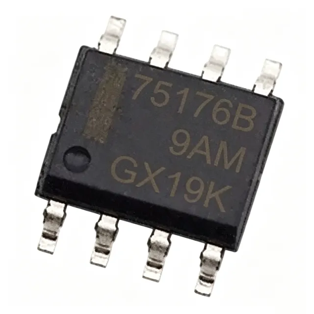
The Texas Instruments TPD4S012DRYR is a 4-channel transient voltage suppressor (TVS) ESD protection diode array purpose-built for USB High-Speed (HS), USB On-The-Go (OTG), and USB charger interfaces. It integrates four 0.8-pF low-capacitance protection channels plus a power-rail clamp with 15-V tolerance on the VBUS line, in an ultra-small flow-through 6-SON (1.45 mm x 1 mm) package rated for IEC 61000-4-2 system-level ESD strikes of ±10 kV (contact/air). An ESD protection diode array is a type of transient voltage suppressor (TVS) within the broader circuit-protection hierarchy: surge protector -> TVS diode -> ESD protection array. Its role is to clamp fast electrostatic-discharge transients before they reach sensitive transceiver silicon, diverting charge to ground or to the supply rail while remaining invisible to the high-speed signal during normal operation. Key differentiating features include: (1) 0.8 pF typical line capacitance, which preserves USB 2.0 high-speed eye diagrams at 480 Mbps with minimal insertion loss; (2) 15-V VBUS tolerance, allowing the power clamp to survive charger voltages and OTG VBUS events that would destroy ordinary 5.5-V clamps on data lines; (3) 3-A (8/20 us) Ipp clamp capability on the power path; and (4) a flow-through package that enables clean differential D+/D- routing without stubs. The device uses snapback-free directional TVS cells on D+/D- and a dedicated zener-based clamp for VBUS, achieving sub-nanosecond response to ESD events per IEC 61000-4-2 testing. Typical applications are smartphone and tablet USB ports, portable charger power paths, USB OTG connectors, and any downstream USB transceiver exposed to user-handled connectors. Design consideration: keep the TPD4S012 within a few millimeters of the connector and place the ground connection to a low-impedance plane; ESD protection effectiveness degrades rapidly with trace inductance. Prices as of 2026-08-29.
TPD4S012DRYR - 4-Ch USB ESD Protection, 15V VBUS | TI
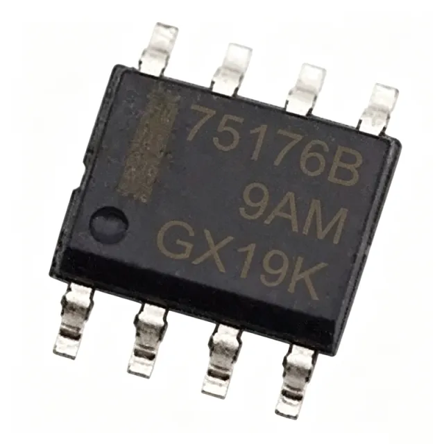
The Texas Instruments TPD4S012DRYR is a 4-channel transient voltage suppressor (TVS) based ESD protection diode array with 0.8-pF line capacitance, ±10-kV IEC 61000-4-2 system-level ESD protection, and 15-V VBUS tolerance, housed in a 6-SON (1.45 mm x 1 mm) surface-mount package. An ESD protection diode array is a specialized category of transient voltage suppressor within the broader circuit-protection hierarchy: surge protector -> TVS diode -> ESD protection array. Its function is to clamp nanosecond-scale electrostatic discharge transients at a connector before they reach sensitive transceiver silicon, diverting charge to ground or the supply rail while remaining electrically invisible to the high-speed signal during normal operation. Key differentiating features include 0.8 pF typical channel capacitance, which preserves USB 2.0 high-speed (480 Mbps) eye diagrams with minimal insertion loss; a dedicated power clamp with 15-V tolerance on the VBUS line, allowing it to survive charger overvoltages and OTG VBUS events that would destroy ordinary 5.5-V data-line clamps; and a 3-A (8/20 us) Ipp clamp capability on the power path. Architecturally, the device combines snapback-free directional TVS cells on D+/D- and ID lines with a zener-based clamp for VBUS, achieving sub-nanosecond response to ESD events per IEC 61000-4-2 testing. The flow-through pinout enables clean differential D+/D- routing without stubs, protecting 3 high-speed I/O lines plus VBUS simultaneously - a combination specifically targeted at USB OTG designs. Typical applications include smartphone and tablet USB ports, portable charger power paths, USB OTG connectors on media players and cameras, and any downstream USB transceiver exposed to user-handled connectors. Design consideration: place the TPD4S012 within a few millimeters of the connector and return its ground pin to a low-impedance plane; protection effectiveness degrades rapidly with added trace inductance. This page synthesizes distributor availability, drop-in alternative analysis, and practical layout guidance not found in the manufacturer datasheet. Pricing shown is estimated as of 2026-09-01.

TVS4201MR6T1G - 5V TVS Array, 12V Clamp, 6-TSOP | onsemi
The onsemi TVS4201MR6T1G is a low-capacitance transient voltage suppressor (TVS) diode array designed to protect high-speed data lines from ESD, EFT, and lightning-induced surges. Housed in a compact 6-pin TSOP-6 (TSOT-23-6) surface-mount package, it integrates a unidirectional 5 V working-voltage TVS array that clamps at 12 V and absorbs up to 25 A of peak pulse current (8/20 µs waveform), making it a drop-in protection block for USB, HDMI, and other consumer interface ports. A TVS (transient voltage suppressor) diode is a specialized clamping device that maintains a near-open circuit under normal operating conditions but rapidly conducts (clamps) when the line voltage exceeds its breakdown threshold, shunting dangerous transients to ground before downstream ICs can be harmed. The TVS4201MR6 family is part of onsemi's low-capacitance portfolio, optimized for high-speed lines where excessive loading capacitance would otherwise degrade signal integrity. Key features include 12 V maximum clamping voltage at 25 A (8/20 µs), 5 V reverse working voltage (Vrwm), an integrated unidirectional TVS array, low line-to-line capacitance suited to high-speed data rates, and an operating temperature range of -40 °C to +125 °C. The 6-TSOP package also meets AEC-Q101 automotive qualification criteria, enabling deployment in body-electronics and infotainment designs alongside consumer applications. The TVS4201MR6T1G uses onsemi's TVS array process that integrates steering diodes in a compact form factor, achieving tight clamping behavior with minimal series inductance. This architecture is purpose-built for transient suppression on differential or single-ended lines where a small PCB footprint and high surge-handling are simultaneously required, reducing the BOM count compared to discrete TVS solutions. Typical applications include USB 2.0/3.0 data-line clamping, HDMI/MHL/MIPI video-interface protection, smartphone charging-port ESD protection, automotive infotainment and body-control ports, and general-purpose I/O protection on microcontroller or SoC pins. Designers favor this part because it provides datasheet-verified surge and ESD immunity in a footprint compatible with industry-standard TSOT-23-6 TVS arrays. For best results, place the TVS as close as possible to the connector and use a low-inductance ground return via multiple vias. Ensure that the trace between the protected IC and the connector is short and direct, with the TVS ground stitch tied to the chassis or system ground rather than the digital ground, to maximize surge dissipation and minimize residual clamping voltage seen by the protected IC. This page synthesizes distributor pricing, AEC-Q101 automotive-grade drop-in alternatives in the same 6-TSOP footprint, and practical PCB-layout design notes not found in the onsemi datasheet, providing engineering value beyond raw specification repetition.

UF3007 - 3A 800V Ultra-Fast Rectifier Diode | Diodes Inc
The Diodes Incorporated UF3007 is a 3.0 A ultra-fast rectifier diode with an 800 V repetitive peak reverse voltage, a 1.7 V maximum forward voltage drop, and a 75 ns reverse recovery time, housed in a DO-201AD (DO-27 style) axial-lead through-hole package. An ultra-fast rectifier is a power semiconductor diode engineered for very short reverse recovery time (trr), which is the interval during which the diode continues to conduct after the applied voltage reverses. Within the power-conversion component hierarchy, the ultra-fast rectifier is a member of the rectifier diode family, which in turn belongs to discrete semiconductors and power management building blocks. Fast recovery matters because slow diodes dissipate significant switching losses in high-frequency converters. Key features of the UF3007 include a diffused-junction construction optimized for high switching efficiency, a surge overload rating of up to 150 A peak (non-repetitive), low reverse leakage current, and a plastic body carrying a UL flammability classification of 94V-0. High current capability combined with low forward voltage drop reduces conduction losses in the output stage. Technical analysis: the 75 ns trr class places the UF3007 well below standard-recovery diodes (microseconds) and suits switching frequencies commonly found in flyback and forward converters. According to the manufacturer datasheet, for capacitive loads the output current should be derated by 20% relative to the resistive-load rating. Storage temperature spans -65C to +175C per typical DO-201AD ratings, enabling rugged industrial designs. Typical applications include secondary-side output rectification in AC-DC switch-mode power supplies, free-wheeling and snubber circuits in motor drives, DC-DC converter output stages, and reverse-polarity protection in industrial equipment. Design consideration: keep lead length short and verify average forward current derating at elevated ambient temperatures, since DO-201AD axial packages rely on lead conduction for heat extraction. This page synthesizes distributor cross-reference data, drop-in alternatives, and practical design notes not found in the manufacturer datasheet alone.

ULC0502P3 - 5V 2-Line Ultra-Low Capacitance TVS | Leiditech
The Shanghai Leiditech Electronic Technology ULC0502P3 is a 2-line ultra-low capacitance transient voltage suppressor (TVS) diode array rated for 5V operating voltage, housed in a 3-pin leadless DFN1006-3 (1.0mm x 0.6mm x 0.5mm) package. It is engineered to protect two high-speed data lines or signal lines from electrostatic discharge (ESD), electrical fast transients (EFT), and lightning-induced surges, while adding minimal parasitic loading to the protected lines. A TVS (Transient Voltage Suppressor) diode is a solid-state semiconductor device designed to clamp voltage spikes and divert transient currents away from sensitive downstream ICs. Within the protection hierarchy (TVS diode -> ESD suppressor -> surge protector -> circuit protection component), TVS diodes sit at the IC-port level and are routinely placed next to USB, HDMI, MIPI, and antenna connectors. Ultra-low capacitance variants like the ULC0502P3 specifically target high-speed signal lines where conventional TVS diodes would degrade signal integrity. Key features of the ULC0502P3 include ultra-low leakage at the nA level, a low 5V operating (working) voltage, low clamping voltage during transient events, and a miniature 3-pin leadless DFN1006-3 footprint. The device is compliant with IEC 61000-4-2 ESD immunity testing at +/-30kV air discharge and +/-25kV contact discharge, with IEC 61000-4-4 EFT immunity at 40A (5/50ns) and IEC 61000-4-5 surge immunity at 5A (8/20us). Lead finish is NiPdAu (nickel-palladium-gold) for reliable soldering and corrosion resistance, and the device is RoHS compliant. The ULC0502P3 is best understood as a two-channel unidirectional low-capacitance ESD diode in a sub-millimeter package, optimized for high-speed signal routing. Compared with general-purpose TVS diodes that may add tens of picofarads of junction capacitance, ultra-low capacitance parts such as this one preserve signal eye-diagram margins on USB 2.0, USB 3.0, HDMI, MIPI DSI/CSI, and other GHz-class interfaces. Typical applications include USB 2.0/3.0 data line protection, HDMI/MIPI display and camera interfaces, smartphone and wearable charging port protection, wireless antenna RF feed protection, and general-purpose I/O protection on microcontrollers and SoCs. Designers frequently pair the ULC0502P3 with common-mode chokes, ferrite beads, and bulk decoupling capacitors to form a complete port protection network. When designing in this part, place it as close as possible to the connector body or IC pin to minimize the parasitic inductance of the protection loop. Use wide, short ground traces to the PCB ground plane to ensure the lowest impedance return path for transient currents, and follow the layout recommendation to keep the protected traces directly under the device body without stubs or vias. This page synthesizes distributor pricing, drop-in alternatives, and practical design notes not found on the Leiditech product page or datasheet, helping engineers shorten the selection cycle and avoid common port-protection pitfalls.