Товары (39.000+)

MT29F4G08ABADAWP-IT:D - 4Gbit SLC NAND Flash Parallel x8 | Micron
MT29F4G08ABADAWP-IT:D

MT29F4G08ABADAWP-IT:D - 4Gbit SLC NAND Flash Parallel x8 | Micron

The Micron MT29F4G08ABADAWP-IT:D is a 4-Gbit (512M x 8) SLC NAND Flash memory device housed in a 48-pin TSOP-I package, designed for industrial-grade embedded storage applications. It features a parallel byte-wide interface operating from a single 2.7V to 3.6V supply, with a 25 ns access time and ONFI 2.1 compliance for standardized command set support. NAND Flash memory is a non-volatile storage technology that retains data without power and uses floating-gate transistors arranged in NAND (series) strings to achieve high density at low cost per bit. SLC (Single-Level Cell) NAND stores one bit per cell, giving it superior endurance (typically 100K P/E cycles), faster write performance, and higher data retention compared to MLC/TLC NAND. Within the memory hierarchy, SLC NAND sits between raw NOR Flash (faster, lower density, byte-erasable) and managed NAND (eMMC/UFS, which integrate a controller). The MT29F4G08A family uses a raw NAND interface requiring an external ECC controller for bad-block management. Key differentiating specifications include 4-Gbit density in x8 (byte-wide) organization, 25 ns tRC access time, 48-pin TSOP-I footprint with 18.40 mm body width, and an extended industrial operating temperature range of -40C to +85C. The device supports multi-plane operations for higher throughput, and its command set complies with the ONFI 2.1 specification, simplifying host-side firmware development across compatible Micron SLC NAND generations. Architecturally, the MT29F4G08ABADAWP-IT:D uses a single-die design with two planes, each containing 2048 blocks of 64 pages x 4 KB + spare area. The 8-bit asynchronous interface uses standard NAND control signals (CE#, RE#, WE#, ALE, CLE) plus R/B# for ready/busy status. Internally generated ECC is not provided - the host must perform error correction over each 512-byte or 4 KB sector according to ONFI timing. Typical applications include industrial routers, automotive infotainment boot/media storage, factory automation data loggers, point-of-sale terminals, set-top box firmware storage, and medical monitoring devices requiring long-term reliability. Designers choose SLC NAND over MLC/TLC when endurance and data integrity outweigh cost-per-bit. When designing with this device, allocate 1KB to 4KB of host-side ECC engine capacity per page (typically BCH or Reed-Solomon) and reserve ~1% of total blocks for spare-area bad-block replacement. Decoupling capacitors of 0.1 uF plus 4.7 uF should be placed within 5 mm of the VCC and VCCQ pins. This page synthesizes distributor pricing, drop-in alternatives, and practical design notes that supplement the manufacturer datasheet with engineering-decision context.

Запрос цены Контакты
MT29F4G08ABAFAH4-IT:F - 4Gb SLC NAND Flash, x8, 63-VFBGA | Micron
MT29F4G08ABAFAH4-IT:F

MT29F4G08ABAFAH4-IT:F - 4Gb SLC NAND Flash, x8, 63-VFBGA | Micron

The Micron MT29F4G08ABAFAH4-IT:F is a 4 Gbit (512 MB) single-level cell (SLC) NAND Flash memory device organized as x8, supplied in a 63-ball VFBGA package, and qualified to the industrial temperature range (-40C to +85C). It conforms to the Open NAND Flash Interface (ONFI) 1.0 specification, exposing a standardized asynchronous command set, and supports a 3.3 V VCC supply typical of parallel NAND devices. A NAND Flash is a non-volatile memory that stores data as charge on a floating-gate MOSFET cell arranged in a NAND string. SLC NAND stores one bit per cell, yielding the highest endurance (typically 100k P/E cycles per block) and the lowest bit error rate among NAND types, making it preferred over MLC/TLC for industrial, automotive, and mission-critical embedded systems. NAND sits below the memory hierarchy above raw NOR and below DRAM in terms of write speed, density, and cost per bit, and is managed by an external controller that performs bad-block management, wear leveling, and ECC. The device is organized as 4352 bytes + 256 bytes of spare per page (x8) and 64 pages per block; with one plane, the 4 Gbit array yields 512 MB user data. CE# Don't Care operation allows the device to share an asynchronous memory bus with other flash or SRAM devices, simplifying glue logic. The 25 ns asynchronous access time keeps the device compatible with legacy microcontrollers, FPGA soft-cores, and Linux boot loaders that lack ONFI 2.x source-synchronous modes. Typical applications include industrial gateways, factory automation PLCs, automotive infotainment and telematics boot media, networking line cards, point-of-sale terminals, and SSD controller raw-NAND banks. The industrial temperature grade extends deployment to outdoor cabinets and uncontrolled enclosures. Designers typically pair the MT29F4G08ABAFAH4-IT:F with a host SoC that includes an ONFI 1.0 controller, plus a BCH or LDPC ECC engine capable of correcting 4-8 bit errors per 512-byte sector. When designing in this device, write down 4-8 bit BCH ECC requirements and verify that the host controller issues CE# Don't Care safely. The 63-VFBGA package demands NSMD pads with 0.4 mm pitch and a reflow profile compatible with JEDEC J-STD-020 moisture sensitivity level 3.

Запрос цены Контакты
MT29F4G16ABADAWP-IT:D - 4Gb SLC Parallel NAND Flash, 48-TSOP I | Micron
MT29F4G16ABADAWP-IT:D

MT29F4G16ABADAWP-IT:D - 4Gb SLC Parallel NAND Flash, 48-TSOP I | Micron

The Micron MT29F4G16ABADAWP-IT:D is a 4-Gbit SLC NAND Flash memory device organized as 256M x 16 bits with a parallel asynchronous interface, housed in a 48-pin TSOP Type I package. It operates from a single 3.3 V supply (2.7 V min to 3.6 V max), supports x8/x16 data bus widths, and provides 25 ns typical access time for high-throughput read/write operations. As a member of the NAND Flash family (subtype: SLC NAND), the MT29F4G16ABADAWP-IT:D belongs to the broader hierarchy of non-volatile memory -> flash memory -> NAND flash -> SLC NAND -> parallel NAND. SLC (Single-Level Cell) NAND stores one bit per cell, offering higher endurance, faster write speeds, and longer data retention than MLC or TLC alternatives, which is why it remains the preferred technology for industrial, automotive, and embedded systems requiring reliable boot/storage media. Key features include on-chip ECC support, an internal data register, command/address/data multiplexed I/O, and a dedicated hardware reset pin (WP#). The TSOP-I 48-pin footprint is the industry-standard pinout that remains consistent across the MT29F4G16 family, enabling drop-in upgrades to higher densities without board rework. Industrial temperature range (-40C to +85C) and 100,000 program/erase cycles per block support harsh-environment deployment. Typical applications span industrial data logging, automotive infotainment, networking routers, set-top boxes, and embedded Linux systems where the host CPU (often an ARM SoC or PIC32MZ MCU) executes XIP-like boot sequences from parallel NAND. The wide VCC tolerance and 25 ns access time also suit legacy PCI/ISA bus adapters and factory automation controllers. When designing with this device, allocate proper ECC handling in software (typically 4-bit/512B BCH or 8-bit/512B BCH depending on host capability) and respect the WE#/RE# toggle timing shown in the AC characteristics table. The 48-TSOP-I footprint is footprint-compatible with several higher-density Micron variants, simplifying future migration to 8 Gb or 16 Gb densities. This page synthesizes distributor pricing, drop-in alternatives, and practical design notes not found in the manufacturer datasheet alone.

Запрос цены Контакты
MT29F64G08AFAAAWP-ITZ:A - 64Gb SLC Parallel NAND Flash 48-TSOP
MT29F64G08AFAAAWP-ITZ:A

MT29F64G08AFAAAWP-ITZ:A - 64Gb SLC Parallel NAND Flash 48-TSOP

The Micron MT29F64G08AFAAAWP-ITZ:A is a 64-Gbit asynchronous SLC NAND Flash memory device organized as 8G x 8 bits, housed in a 48-pin TSOP type-I (0.5 mm pitch) package. Operating from a 2.7 V to 3.6 V supply and based on Micron's 25 nm SLC NAND process, this industrial-temperature (IT) part is designed for embedded and high-reliability designs that require predictable endurance and data retention. A NAND Flash memory is a non-volatile storage technology that retains data without power and is organized as an array of memory cells connected in series (strings) per bitline, with each cell storing charge on a floating gate. SLC (Single-Level Cell) NAND stores one bit per cell, delivering the highest endurance and lowest bit-error-rate of any NAND technology. In the broader hierarchy, this device is a parallel (asynchronous) NAND IC, which sits below managed NAND (eMMC, UFS) but above serial NOR flash in capacity and below DRAM in performance. Key specifications include a 64-Gbit density (8 GB), 8-bit bus width, ONFI 1.0-compatible asynchronous interface, typical page size of 8 Kbytes (plus spare), 25 ns typical access time, and industrial temperature range of -40 C to +85 C. The 48-TSOP I package is a 12 mm x 20 mm surface-mount form factor that has been the industry-standard pinout for parallel NAND for two decades. The device uses Micron's two-plane architecture with interleaved plane operations to maximize sequential write bandwidth. Built-in ECC is required externally (typically BCH or LDPC in the host controller). The industrial-temperature grade and SLC endurance make this part well suited to systems that cannot tolerate the higher bit-error rate of MLC or TLC NAND. Typical applications include industrial embedded controllers, networking line cards with boot storage, automotive infotainment (where AEC-Q100 is not required), factory automation PLCs, and legacy designs that already have a parallel NAND controller and ECC engine. The 48-TSOP form factor is also commonly used in set-top boxes and printers. When designing with this part, ensure the host controller supplies a 1.8 V or 3.3 V Vccq and routes 8-bit data with impedance-controlled traces. The WP#, CE#, ALE, CLE, RIO, and R/B pins must be tied or driven correctly to avoid bus contention during power-up. This page synthesizes real-time distributor pricing, verified drop-in alternatives, and practical design notes that go beyond the manufacturer datasheet.

Запрос цены Контакты
MT29F8G16ADBDAH4-IT:D - 8Gb x16 SLC NAND Flash, 1.8V | Micron
MT29F8G16ADBDAH4-IT:D

MT29F8G16ADBDAH4-IT:D - 8Gb x16 SLC NAND Flash, 1.8V | Micron

The Micron MT29F8G16ADBDAH4-IT:D is an 8Gb SLC NAND Flash memory device organized as 512M x 16 bits, housed in a 63-ball VFBGA (9x11 mm) package with parallel interface and 25 ns access time. It operates from a 1.8V supply (1.7V min / 1.95V max) across an industrial temperature range of -40C to +85C, and uses Micron's reliable single-level-cell NAND architecture for high endurance and predictable read/write performance. An SLC (Single-Level Cell) NAND flash is a non-volatile memory that stores one bit per memory cell, providing higher write endurance, faster write speeds, and longer data retention than MLC/TLC counterparts. NAND Flash sits below NOR Flash in the storage hierarchy, optimized for high-density sequential and page-based access in embedded systems, automotive infotainment, industrial gateways, and boot/media storage subsystems where reliability and bit-level integrity outweigh raw cost-per-bit. Key features include 8Gbit density (1 Gbyte), x16 data bus for high-throughput parallel access, ONFI-compatible asynchronous interface, internal data ECC support per page, and a 63-VFBGA surface-mount package suitable for compact, reflow-solderable embedded designs. The device supports standard NAND command set (read, program, erase, status read, ID read) and operates from a single 1.8V Vcc rail. The MT29F8G16ADBDAH4-IT:D uses Micron's 4Gb/8Gb/16Gb NAND flash die platform, leveraging proven floating-gate SLC cell technology and a mature CMOS process. Page size is typically 2048 bytes + 64 bytes spare (for x16), supporting partial-page programming and block erase. The parallel interface allows direct connection to microcontrollers, application processors, and FPGAs without external glue logic. Typical applications include automotive infotainment and telematics storage, industrial control/IIoT gateways, networking equipment (switches/routers for OS images and logs), point-of-sale terminals, medical data recorders, and Linux/Android embedded boot or mass-storage subsystems requiring reliable, industrial-temperature non-volatile memory. When designing with this part, ensure proper signal integrity on the parallel data bus, respect Vcc ramp sequencing, and implement software or hardware ECC for data integrity. The compact 9x11 mm VFBGA footprint simplifies PCB layout but requires careful fan-out and via-in-pad or microvia design for reliable manufacturability. This page synthesizes distributor pricing, drop-in compatible alternatives across Micron and competing vendors, application guidance, and practical PCB/thermal design notes beyond the manufacturer datasheet to accelerate your embedded storage design.

Запрос цены Контакты
MT40A1G16KNR-075-IT-E - 16Gb DDR4-2666 1Gx16 SDRAM | Micron
MT40A1G16KNR-075-IT-E

MT40A1G16KNR-075-IT-E - 16Gb DDR4-2666 1Gx16 SDRAM | Micron

The Micron MT40A1G16KNR-075-IT-E is a 16-Gbit DDR4 SDRAM organized as 1G words × 16 bits, packaged in a 96-ball Fine-Pitch BGA (FBGA, 7.5 mm × 13.5 mm × 1.1 mm) with a -075 speed bin corresponding to DDR4-2666 (1600 MHz clock, 2666 MT/s data rate). It operates from a 1.2 V nominal VDD supply (1.14 V to 1.26 V per Micron's datasheet) with VDDQ at 1.2 V and a VPP supply of 2.5 V, and uses a dual-die-package (DDP) stack to reach 16 Gb density in a single chip. A DDR4 SDRAM is a synchronous dynamic random-access memory that quadruples the data rate of DDR3 by transferring data on both clock edges and using a pseudo-open-drain SSTL_12 I/O standard with on-die termination. As a member of the broader DRAM family, DDR4 SDRAM occupies the mainstream volatile main-memory segment used in servers, workstations, embedded computing platforms, and high-end networking gear, sitting between the LPDDR/low-power DRAM family (mobile) and HBM (high-bandwidth, high-end accelerators) in the JEDEC memory taxonomy. Key features include a 1.07 GHz / 1.33 GHz maximum clock frequency per Micron product pages, 19 ns CAS latency timing budget, on-die temperature sensor with automatic self-refresh, ZQ calibration for output-driver impedance trimming, and a programmable MR (mode-register) interface that supports fine-grained timing, refresh, and voltage tuning. The IT industrial temperature grade spans 0 °C to +95 °C (this is the E-grade base temperature; see validation for the IT industrial note), and the device is JEDEC JESD79-4 DDR4 compliant. Architecturally, the die uses Micron's 20 nm-class DRAM process and integrates 8 internal banks with bank-grouping for improved throughput. The 16-bit data interface and ×16 organization make the part well suited for high-bandwidth applications where parallel channels are limited, such as AI accelerator boot memory and FPGA-attached DRAM buffers. Typical applications include AI server boot memory, BMC/management-controller DRAM, storage-controller cache (SAS/NVMe RAID HBAs), embedded computing modules, FPGA SoC attached memory, and service-spare DDR4 inventory for hyperscaler maintenance. When designing with this part, observe the PCB routing rules in Micron's TN-40-series application notes: maintain 90 Ω differential impedance on the DQ/DQS pairs, length-match the byte lane within ±25 ps, and provide a clean 2.5 V VPP rail with at least 10 µF of decoupling near each device. This page synthesizes distributor pricing, drop-in same-package and cross-brand alternatives, and PCB design guidance not found in the manufacturer datasheet alone.

Запрос цены Контакты
MT40A1G8AG-062E AUT:R - 8Gb DDR4-3200 x8 78-FBGA | Micron
MT40A1G8AG-062E AUT:R

MT40A1G8AG-062E AUT:R - 8Gb DDR4-3200 x8 78-FBGA | Micron

The Micron MT40A1G8AG-062E AUT:R is an automotive-grade 8 Gbit DDR4 SDRAM organized as 1G x 8, housed in a 78-ball Fine-Pitch Ball Grid Array (FBGA, 7.5 x 11 mm) and qualified to AEC-Q100 for in-vehicle electronic systems. It operates from a 1.2 V VDD/VDDQ supply and clocks up to 1600 MHz (DDR4-3200 data rate), delivering a maximum access time of 19 ns. The device ships in Tape-and-Reel packaging with the AUT suffix denoting automotive temperature grade and the R suffix denoting the reel pack orientation. DDR4 (Double Data Rate 4) SDRAM is the fourth generation of synchronous DRAM, succeeding DDR3 by doubling the minimum data rate, lowering the I/O voltage to 1.2 V from 1.5 V, and introducing bank-grouping for higher effective bandwidth at lower power. Within the broader memory hierarchy, DDR4 sits between LPDDR4 mobile DRAM and HBM stacked memory, targeting compute-heavy platforms that need high throughput and moderate cost. The 1G x 8 organization gives one byte-wide data bus plus an 8-bit-deep chip ID, which is the most common building block for populating byte lanes in controller-driven ECC or non-ECC systems. Key features of this part include on-die termination (ODT), write leveling, ZQ calibration, an integrated temperature sensor, and a bank-group architecture that lowers latency at high burst rates. Automotive qualification to AEC-Q100, support for -40C to +95C case temperature, and PPAP documentation make the AUT suffix suitable for ADAS, infotainment, and digital cockpit SoCs. Internally, the die uses a 20 nm-class process with a 16-bank / 4-bank-group architecture and a high-speed pseudo-open-drain POD interface, which lowers switching noise and enables data rates of 3200 MT/s while staying within 1.2 V I/O. A parity-based command/control path protects against command bus errors during fast burst operations. On-system calibration of ODT impedance, VrefDQ, and write leveling is handled by the host controller in conjunction with the part's MR registers. Typical applications for the MT40A1G8AG-062E AUT:R include automotive ADAS controllers, digital cockpit and infotainment SoCs, in-vehicle networking gateways, and ruggedized industrial edge platforms. The AEC-Q100 qualification also makes it a viable drop-in for fleet management and telematics modules where commercial-grade DRAM would otherwise require additional environmental re-qualification. When laying out the PCB, follow Micron's 78-ball FBGA escape pattern, provide matched-length data byte lanes, and place the 240 ohm ZQ reference resistor within 5 mm of the package ball. Maintain proper decoupling - 0.1 uF and 10 uF capacitors per VDD/VDDQ rail - to keep switching noise within DDR4 spec during write bursts.

Запрос цены Контакты
MT40A1G8SA-075:E - 8Gb DDR4 SDRAM 1.33GHz | Micron
MT40A1G8SA-075:E

MT40A1G8SA-075:E - 8Gb DDR4 SDRAM 1.33GHz | Micron

The Micron MT40A1G8SA-075:E is a high-performance DDR4 SDRAM component organized as 1G x 8, providing 8Gbit of memory density. It operates at a clock speed of 1.33 GHz (DDR4-2666) with a parallel interface, housed in a compact 78-ball FBGA package measuring 7.5x11 mm. This device is designed for a wide range of computing, networking, and industrial applications requiring high bandwidth and low power consumption. DDR4 SDRAM (Double Data Rate 4 Synchronous Dynamic Random-Access Memory) is a type of volatile memory that transfers data on both rising and falling edges of the clock signal, effectively doubling the data rate. It is the fourth generation of DDR memory, succeeding DDR3, and offers higher speed, lower operating voltage (1.2V), and improved power efficiency. DDR4 is a critical component in modern computing systems, servers, and embedded devices, forming the main memory hierarchy alongside storage and cache. Key features of the MT40A1G8SA-075:E include a supply voltage of VDD = VDDQ = 1.2V ±60mV, with VPP at 2.5V (-125mV, +250mV). It supports on-die, internal, adjustable VREFDQ generation and 1.2V pseudo open-drain I/O. The device offers a refresh time of 8192 cycles with temperature-dependent refresh rates: 64ms at -40°C to 85°C, 32ms at >85°C to 95°C, and 16ms at >95°C to 105°C. Additional features include write leveling, dynamic on-chip termination, CRC function, and data mask function, ensuring signal integrity and reliable operation. Technically, the MT40A1G8SA-075:E utilizes Micron's advanced DRAM process technology, achieving high density and performance while maintaining low power. The 78-ball FBGA package with a 7.5x11 mm footprint is optimized for space-constrained PCB designs, offering excellent thermal and electrical characteristics. The device supports a data rate of 2666 MT/s, providing a peak bandwidth of 21.3 GB/s per module (when paired with a 64-bit bus). Typical applications include high-performance computing, servers, networking equipment (routers, switches), and industrial automation systems. Its high speed and reliability make it suitable for memory-intensive tasks such as data analytics, virtualization, and real-time processing. The low operating voltage contributes to energy-efficient designs, crucial for data centers and battery-powered devices. When designing with this component, ensure proper decoupling capacitors near the power pins and follow the layout guidelines in the Micron datasheet to minimize signal integrity issues. The device requires a stable 1.2V supply and careful attention to the VPP rail for optimal performance.

Запрос цены Контакты
MT40A1G8WE-075E - 8Gb DDR4 SDRAM 1.33GHz | Micron
MT40A1G8WE-075E

MT40A1G8WE-075E - 8Gb DDR4 SDRAM 1.33GHz | Micron

The Micron MT40A1G8WE-075E is a high-performance DDR4 SDRAM component organized as 1G x 8, providing 8Gbit of memory density. It operates at a clock speed of 1.33 GHz (DDR4-2666) and is housed in a compact 78-ball FBGA (8x12mm) package, making it suitable for space-constrained applications requiring high bandwidth and low power consumption. DDR4 SDRAM (Double Data Rate 4 Synchronous Dynamic Random-Access Memory) is the fourth generation of DDR memory, offering higher speed and lower power than its predecessors. It uses a 1.2V supply (VDD and VDDQ) with a separate 2.5V VPP for wordline boost, and features on-die termination (ODT), internal VREFDQ generation, and pseudo-open-drain I/O. DDR4 achieves data rates up to 3200 MT/s, with the -075E speed grade indicating 2666 MT/s operation. Key features include a refresh time of 8192 cycles at TC temperature range: 64ms at -40°C to 85°C, 32ms at >85°C to 95°C, and 16ms at >95°C to 105°C. The device supports on-die, internal, adjustable VREFDQ generation and 1.2V pseudo-open-drain I/O. It is available in industrial temperature grades (AIT) and standard temperature grades, with options for automotive (AEC-Q100) qualification in some variants. Technically, the MT40A1G8WE-075E utilizes Micron's advanced DRAM process technology, achieving high density with low power consumption. The 78-ball FBGA package provides excellent thermal and electrical performance, with a ball pitch of 0.8mm. The device supports burst lengths of 8 and 4, and features programmable CAS latency, additive latency, and write recovery time. Typical applications include servers, networking equipment, high-performance computing, and embedded systems requiring high memory bandwidth. The 1G x 8 organization is ideal for error-correcting code (ECC) modules and systems with multiple memory channels. When designing with this component, ensure proper decoupling capacitors near the VDD and VDDQ pins, and follow Micron's layout guidelines for DDR4 routing to maintain signal integrity at 2666 MT/s.

Запрос цены Контакты
MT40A256M16GE-075E AAT:B - 4Gb DDR4 SDRAM 256Mx16 96-FBGA | Micron
MT40A256M16GE-075E AAT:B

MT40A256M16GE-075E AAT:B - 4Gb DDR4 SDRAM 256Mx16 96-FBGA | Micron

The Micron MT40A256M16GE-075E AAT:B is a 4 Gbit DDR4 SDRAM organized as 256M x 16 bits, operating at a 1.33 GHz clock frequency (DDR4-2666 speed grade, -075E timing) and housed in a 96-ball Fine-pitch Ball Grid Array (FBGA) measuring 9x14 mm. The part carries the AAT suffix designating automotive-grade qualification (AEC-Q100) and is supplied on tape and reel (TR suffix) for high-volume surface-mount assembly. DDR4 SDRAM (Double Data Rate 4 Synchronous DRAM) is the fourth generation of DDR memory, introduced in 2014 as the successor to DDR3. It doubles the data rate per pin compared with DDR3, operates at a lower 1.2 V VDD/VDDQ supply (versus 1.5 V for DDR3), and introduces POD (Pseudo Open Drain) signalling, bank-grouping, and finer-grained refresh. DDR4 occupies the position DRAM -> volatile memory -> memory IC -> semiconductor in the component hierarchy and remains the dominant PC/server/embedded DRAM standard as of 2026, coexisting with the newer DDR5 in mainstream compute. Key features of the MT40A256M16GE-075E AAT:B include a 1.33 GHz maximum clock rate translating to 2666 MT/s peak transfer rate, a 1.14 V to 1.26 V supply-voltage window (1.2 V nominal), and a parallel interface supporting x16 data width. The die is organized as 8 banks with bank-grouping for improved concurrency, and on-die termination (ODT) is included for signal-integrity control. Temperature-controlled refresh (TCR) is supported to lower self-refresh current at moderate temperatures. The 96-FBGA (9x14 mm) footprint follows the JEDEC-standard x16 DDR4 outline, enabling PCB layout compatibility with industry-standard 4 Gbit x16 DDR4 parts. Architecturally, this device uses Micron's advanced 20 nm-class process node and a sub-byte-write capable 16-bit I/O. The -075E speed sort yields a tCK of 0.75 ns (1333 MHz base, 2666 MT/s effective). On-chip DLL and 1.2 V VPP support simplify board design versus legacy DDR3 platforms that need 2.5 V VPP. Typical applications include automotive infotainment, digital instrument clusters, ADAS compute platforms, industrial embedded controllers, and ruggedized networking gear where AEC-Q100 reliability is mandated. The wide 256M x 16 organization suits frame-store, lookup-table memory, and graphics frame buffers. The AAT suffix denotes the automotive temperature grade (-40C to +105C), and the AAT:B marking indicates lead-free RoHS compliance. A key design consideration is that this part is reported by Micron as obsolete/legacy in their part catalog (referenced May 2026); engineering teams planning new designs should evaluate MT40A256M16GE-075E-IT (industrial) or -AUT (extended automotive) suffixes, or migrate to MT40A512M16 DDR4 8 Gbit or 16 Gbit density migration paths. Signal-integrity, terminations, and VTT must follow JEDEC DDR4 layout rules. This page synthesizes distributor pricing, drop-in alternatives (including the verified HGCHIPS HGD44G16M26 cross-vendor replacement), and engineering guidance not found in the standalone manufacturer datasheet.

USD $6,56 В наличии
MT40A256M16GE-083E - DDR4 4Gb 256Mx16 2400MHz DRAM | Micron
MT40A256M16GE-083E

MT40A256M16GE-083E - DDR4 4Gb 256Mx16 2400MHz DRAM | Micron

The Micron Technology MT40A256M16GE-083E is a 4 Gbit DDR4 SDRAM organized as 256M x 16, operating at a 1200 MHz clock (DDR4-2400 data rate) from a single 1.2 V supply, housed in a 96-ball FBGA package measuring 9 x 14 mm. DDR4 SDRAM (Double Data Rate 4 Synchronous Dynamic Random Access Memory) is the fourth generation of DDR DRAM, sitting in the memory hierarchy above DDR3 and below DDR5. It is a volatile semiconductor memory that stores each bit in a capacitor-based cell refreshed at regular intervals. Compared with DDR3, DDR4 lowers the operating voltage from 1.5 V to 1.2 V, doubles the bank count to 16 (with bank groups), and raises peak data rates to 3200 MT/s and beyond, making it the dominant main-memory technology for embedded and server platforms of its generation. Key features of this device include a 4 Gbit density in a wide x16 organization suited to controllers with 16-bit memory buses, the DDR4-2400 speed grade (CL17 at 1.2 V per JEDEC speed bin -083E), and low-power features such as DLL-off mode and max power-down. The 96-ball FBGA (9 x 14 mm) footprint is the industry-standard package for x16 DDR4 components, enabling second-source layouts. Architecturally, the device is organized into bank groups that allow faster random column access through fine-grained interleaving, and it implements on-die termination (ODT) to preserve signal integrity on high-speed fly-by routed command/address buses. Typical applications include embedded industrial controllers, networking equipment line cards, set-top boxes, and automotive/telematics head units where 16-bit-wide DDR4 interfaces are common. Design consideration: DDR4 fly-by routing requires careful length matching and VTT termination on address/command lines; consult the Micron DDR4 system design guide for VTT and on-die termination settings. This page synthesizes distributor pricing, cross-referenced drop-in alternatives (Samsung, Nanya, and Micron speed/grade variants), and practical design notes not found in the manufacturer datasheet.

Запрос цены Контакты
MT40A512M16HA-083E - 8Gb DDR4-2400 SDRAM | Micron
MT40A512M16HA-083E

MT40A512M16HA-083E - 8Gb DDR4-2400 SDRAM | Micron

The Micron Technology MT40A512M16HA-083E is an 8Gbit DDR4 SDRAM organized as 512M x 16, operating at a 1.2 GHz data rate equivalent to DDR4-2400 and packaged in a 96-ball FBGA measuring 9 x 14 mm. It is designed for systems requiring high-bandwidth volatile memory in a compact surface-mount package. DDR4 SDRAM, or Double Data Rate 4 Synchronous Dynamic Random-Access Memory, is volatile memory that transfers data on both edges of the clock. It belongs to the SDRAM and DRAM hierarchies and operates from a lower core voltage than DDR3 while supporting higher data throughput. DDR4 memory is widely used in servers, networking equipment, data storage systems, and industrial computing platforms. The MT40A512M16HA-083E provides an 8Gbit density with a 16-bit parallel data bus. Its 1.2V VDD and VDDQ supply, 2.5V VPP supply, 1.2V pseudo open-drain I/O interface, and internal adjustable VREFDQ generation support modern DDR4 signal-integrity requirements. Micron specifies a 1.2V supply tolerance of plus or minus 60mV and VPP tolerances from -125mV to +250mV. Refresh timing is temperature dependent. The device uses an 8192-cycle refresh interval, with stated refresh times of 64 ms from -40 degrees C to 85 degrees C, 32 ms above 85 degrees C to 95 degrees C, and 16 ms above 95 degrees C. The 96-ball FBGA uses a 0.8 mm ball pitch and is intended for surface-mount assembly. Typical applications include high-performance servers, routers, switches, storage systems, and industrial platforms. The x16 organization enables practical memory-controller configurations where wider logical channels can be built from multiple devices. PCB implementation should follow Micron's DDR4 layout guidance, including controlled-impedance routing, careful fly-by topology, and placement of decoupling and command/address termination networks close to the memory device. A stable, low-noise 1.2V rail and a compliant 2.5V VPP supply are essential. This page combines manufacturer specifications, distributor references, replacement analysis, and practical DDR4 design guidance to support component selection and board-level implementation.

Запрос цены Контакты
MT40A512M16HA-083E:A - 8Gb DDR4 512Mx16 SDRAM | Micron
MT40A512M16HA-083E:A

MT40A512M16HA-083E:A - 8Gb DDR4 512Mx16 SDRAM | Micron

The Micron Technology MT40A512M16HA-083E:A is an 8Gb DDR4 SDRAM organized as 512M x 16, operating at 1.2 GHz in a 96-ball FBGA (9x14) package. It is designed for systems requiring parallel DDR4 memory with a 1.14 V to 1.26 V supply range and an industrial temperature grade of 0C to +95C. DDR4 SDRAM is a volatile memory technology that stores data in an array of cells and refreshes its contents periodically to maintain data retention. Within the memory hierarchy, DDR4 SDRAM is a high-capacity working-memory component used by computer processors, embedded systems, networking equipment, and industrial controllers. The MT40A512M16HA-083E:A combines a 512M x 16 organization with DDR4 timing and interface features intended for reliable high-bandwidth embedded applications. The verified distributor and manufacturer listings identify this part as an 8Gbit, 512Mx16 DDR4 SDRAM with a 1.2 GHz data rate, 1.14 V to 1.26 V operating voltage, and a 96-FBGA (9x14) package. The x16 organization provides a wider data path than x8 devices when used in systems whose memory controller supports the corresponding organization. The exact speed-bin, timing, voltage, and temperature details should be confirmed against the current Micron datasheet before layout or firmware qualification. This memory is suited to embedded processors, industrial controllers, communications equipment, data-acquisition systems, and other applications that use DDR4 SDRAM directly or through a compatible memory controller. The 96-ball FBGA package requires careful PCB escape routing, power-delivery design, and thermal analysis. Because DRAM packages are sensitive to voltage noise and signal integrity, follow the manufacturer’s reference layout and power recommendations rather than relying on generic BGA rules. The main design consideration is ensuring that the memory controller, board layout, voltage rails, and firmware memory timing all support the selected DDR4 device and operating conditions. The part number suffix identifies the vendor ordering configuration, so designers should verify package orientation, ball assignments, and temperature requirements during procurement and validation. This page combines verified distributor specifications, manufacturer references, cross-reference results, and practical integration guidance to support component selection. Unlike a standalone register or interface IC, this device is a high-density, volatile memory component whose behavior depends strongly on system-level memory design. Use the exact Micron part documentation as the authoritative source for electrical, timing, mechanical, and reliability limits before production release.

Запрос цены Контакты
MT40A512M16JY-075E - 8Gb DDR4 SDRAM 512Mx16 | Micron
MT40A512M16JY-075E

MT40A512M16JY-075E - 8Gb DDR4 SDRAM 512Mx16 | Micron

The Micron MT40A512M16JY-075E is a high-performance DDR4 SDRAM component organized as 512M x 16, providing 8Gbit of memory density. It operates at a clock frequency of 1.33 GHz (DDR4-2666) and is housed in a 96-ball FBGA (8x14) package, designed for surface mounting. This memory IC supports a supply voltage of 1.14V to 1.26V for VDD and VDDQ, with VPP at 2.5V (-125mV, +250mV). It features on-die, internal, adjustable VREFDQ generation and 1.2V pseudo open-drain I/O, making it suitable for a wide range of computing and embedded applications. DDR4 SDRAM (Double Data Rate 4 Synchronous Dynamic Random-Access Memory) is a type of volatile memory that transfers data on both edges of the clock signal, doubling the data rate compared to single-data-rate SDRAM. It is the fourth generation of DDR memory, offering higher speed, lower power consumption, and increased density compared to DDR3. DDR4 operates at a lower voltage (1.2V) than DDR3 (1.5V), reducing power consumption and heat generation. It is widely used in servers, desktops, laptops, and embedded systems where high bandwidth and capacity are required. Key features of the MT40A512M16JY-075E include a refresh time of 8192 cycles, with 64ms at -40°C to 85°C, 32ms at >85°C to 95°C, and 16ms at >95°C. It supports auto precharge, data mask, dynamic on-chip termination, write leveling, auto self-refresh, and CRC functions. The device is RoHS compliant and operates over a temperature range of 0°C to +95°C (TC). These features ensure reliable operation in demanding environments. Technically, the MT40A512M16JY-075E utilizes Micron's advanced DRAM process technology, enabling high-speed data transfer with low power consumption. The 96-ball FBGA package provides excellent thermal and electrical performance, with a compact footprint suitable for space-constrained designs. The device supports a parallel interface, simplifying integration with memory controllers. Typical applications include high-performance computing, servers, networking equipment, and industrial systems where high memory bandwidth and capacity are critical. The 512M x 16 organization is ideal for systems requiring 16-bit data bus width, such as embedded processors and FPGAs. When designing with this component, ensure proper decoupling capacitors are placed near the VDD and VDDQ pins to minimize noise. Follow the PCB layout guidelines in the Micron DDR4 datasheet to maintain signal integrity at high speeds.

Запрос цены Контакты
MT40A512M16JY-07EAIT:B - 8Gb DDR4 SDRAM 512Mx16 | Micron
MT40A512M16JY-07EAIT:B

MT40A512M16JY-07EAIT:B - 8Gb DDR4 SDRAM 512Mx16 | Micron

The Micron MT40A512M16JY-07EAIT:B is a high-performance DDR4 SDRAM component organized as 512M x 16, providing 8Gbit of memory density. It operates at a clock frequency of 1.33 GHz (DDR4-2666) and is housed in a 96-ball FBGA (8x14) package. This device is designed for a wide range of computing, networking, and industrial applications requiring high bandwidth and reliability. DDR4 SDRAM (Double Data Rate 4 Synchronous Dynamic Random-Access Memory) is a type of volatile memory that transfers data on both edges of the clock signal, effectively doubling the data rate. It operates at a lower voltage (1.2V) compared to DDR3 (1.5V), reducing power consumption while offering higher speed and density. DDR4 is the industry standard for modern servers, desktops, and embedded systems, providing a balance of performance, capacity, and energy efficiency. Key features of the MT40A512M16JY-07EAIT:B include a supply voltage of VDD = VDDQ = 1.2V ±60mV, VPP = 2.5V, and on-die, internal, adjustable VREFDQ generation. It supports 1.2V pseudo open-drain I/O and has a refresh time of 8192 cycles at TC temperature range: 64ms at -40°C to 85°C, 32ms at >85°C to 95°C, and 16ms at >95°C to 105°C. The device is AEC-Q100 qualified (indicated by the 'AIT' suffix), making it suitable for automotive applications. The MT40A512M16JY-07EAIT:B utilizes Micron's advanced DRAM process technology, offering high reliability and performance. It features programmable data strobe preambles, on-die termination (ODT), and write leveling for improved signal integrity. The 96-ball FBGA package provides a compact footprint while enabling high-speed operation with minimal parasitic inductance. Typical applications include automotive advanced driver-assistance systems (ADAS), infotainment systems, networking equipment, servers, and high-performance computing. Its automotive qualification and wide temperature range make it ideal for under-the-hood and in-cabin electronics. When designing with this device, ensure proper decoupling capacitors are placed close to the VDD and VDDQ pins to minimize power supply noise. Follow Micron's layout guidelines for DDR4 routing to maintain signal integrity at 1.33 GHz.

Запрос цены Контакты
MT40A512M16LY-062E AAT:E - 8Gbit DDR4 SDRAM 1.6GHz | Micron
MT40A512M16LY-062E AAT:E

MT40A512M16LY-062E AAT:E - 8Gbit DDR4 SDRAM 1.6GHz | Micron

The Micron Technology MT40A512M16LY-062E AAT:E is an 8Gbit DDR4 SDRAM memory IC organized as 512M x 16, operating from a 1.2V supply at a clock frequency of up to 1.6 GHz (DDR4-3200 data-rate class, 062E speed grade, CL19-class latency) with a 19 ns access time, housed in a 96-ball FBGA (7.5 x 13.5 mm) surface-mount package. DDR4 SDRAM (Double Data Rate 4 Synchronous Dynamic Random Access Memory) is the fourth generation of the JEDEC DDR memory family used as the main system memory in computers, servers, and embedded processors. Within the memory hierarchy, DRAM sits between CPU caches and mass storage, and DDR4 succeeds DDR3 with lower operating voltage (1.2V vs 1.5V), higher data rates, bank groups, and improved signaling such as DBI and CA parity. A memory IC like this one is a core component of the semiconductor memory product family under the broader dynamic RAM category. Key features of this device include 8Gbit density in a single x16-wide organization, a 1.2V core supply that reduces dynamic power versus DDR3, an industrial-relevant operating range per the AAT:E ordering code, and the compact 96-FBGA package that supports high-density memory subsystems. The 062E speed bin supports data transfer at DDR4-3200 class rates with a 19 ns access time. Architecturally, the device implements DDR4 bank groups, on-die termination (ODT), and a parallel interface, allowing burst transfers on both clock edges for maximum bandwidth. The x16 organization simplifies single-device designs where x4/x8 server RDIMM topologies are unnecessary, making it popular in embedded and industrial designs that require a single 1 GB-class DRAM. Typical applications include industrial controllers and edge compute modules, networking equipment line-card memory, and embedded processor boards pairing with SoCs that expose a DDR4 x16 controller. Designers choose the x16 organization to achieve 1 GB of DRAM with one BGA footprint. A key design consideration is signal integrity: DDR4 fly-by or point-to-point routing requires length-matched traces, controlled impedance, and proper VTT termination, and the 1.2V rail should be sourced from a DDR-capable PMIC. Confirm the exact speed bin and temperature rating in the manufacturer datasheet before production. This page adds value beyond the datasheet by consolidating distributor pricing as of 2026-09-02, drop-in alternatives from the same package family, and practical DDR4 layout guidance in one place.

Запрос цены Контакты
MT40A512M16LY-062E-ATE - 8Gb DDR4-3200 SDRAM | Micron
MT40A512M16LY-062E-ATE

MT40A512M16LY-062E-ATE - 8Gb DDR4-3200 SDRAM | Micron

The Micron MT40A512M16LY-062E-ATE is an 8 Gb DDR4 SDRAM organized as 512M x 16 with a 1.6 GHz (DDR4-3200) clock rate, 19 ns access time, and 1.2 V nominal supply, housed in a 96-ball FBGA (7.5 x 13.5 mm) package. The -062E speed grade denotes 0.625 ns tCK (DDR4-3200) operation, and the AT suffix marks the automotive temperature range of -40C to +105C. DDR4 SDRAM (Double Data Rate 4 Synchronous Dynamic Random-Access Memory) is the fourth generation of high-bandwidth volatile memory, transferring data on both the rising and falling edges of the clock. It sits in the memory hierarchy between on-chip SRAM and non-volatile storage, and within the broader taxonomy it is a DRAM component -> volatile memory IC -> memory IC -> semiconductor. DDR4 introduced a 1.2 V supply (down from 1.5 V in DDR3), a 16n prefetch architecture, bank groups, and per-bit data bus inversion, all of which raise bandwidth while lowering energy per bit. Key features of the MT40A512M16LY-062E-ATE include 8 Gb density in a single x16 die, 1.6 GHz clock (3200 MT/s), 19 ns access time, 1.2 V VDD with 2.5 V VPP, on-die termination (ODT), write leveling, ZQ calibration, CRC and data-mask functions, and auto self-refresh. The 96-ball FBGA uses a 0.8 mm ball pitch and is footprint-compatible across Micron's 8 Gb x16 DDR4 family, allowing board re-use across speed and temperature grades. The device is built on Micron's advanced DRAM process and is qualified for automotive applications, making it suitable for ADAS domain controllers, automotive infotainment head units, industrial machine vision, and networking line cards. Its 3200 MT/s data rate delivers 6.4 GB/s per x16 device, and the -40C to +105C range supports under-hood and harsh-environment designs. When designing with this part, verify that the memory controller supports DDR4-3200 at the target temperature grade and budget for fly-by routing with VTT termination on the address/command bus. This page synthesizes distributor pricing, drop-in alternatives, and practical design notes not found in the manufacturer datasheet.

Запрос цены Контакты
MT40A512M16LY-062E:E - 8Gb DDR4-3200 x16 SDRAM | Micron
MT40A512M16LY-062E:E

MT40A512M16LY-062E:E - 8Gb DDR4-3200 x16 SDRAM | Micron

The Micron MT40A512M16LY-062E:E is an 8-Gbit DDR4 SDRAM organized as 512M x 16, delivered in a 96-ball TFBGA (7.5 x 13.5 mm) package and rated for DDR4-3200 operation (1600 MHz clock, 3200 MT/s data rate, -062E speed grade). It operates from a 1.2 V VDD core with a 0.6 V VPP high-voltage swing for the DDR4-defined VPP/word-line boost, and integrates on-die termination (ODT), write leveling, ZQ calibration, programmable data strobe (DQS) preamble training, CRC on the data channel, data bus inversion (DBI), and on-chip voltage regulation via the 2.5 V VDDQ / VDD / VPP / VSSQ architecture common to JEDEC JESD79-4 DDR4 SDRAM. A DDR4 SDRAM is a synchronous dynamic random-access memory that uses an 8n-prefetch architecture, dual-rank or single-rank banking, and a bank-group topology introduced in the JEDEC JESD79-4 standard. In the modern memory hierarchy, DDR4 sits between LPDDR4 (mobile, low power) and HBM (high bandwidth, stacked) as the mainstream workhorse DRAM for servers, desktops, embedded computing, and networking. Each generation introduces tighter timing budgets, lower voltage rails, and higher peak transfer rates; DDR4-3200 doubles the peak transfer rate of DDR3-1600 while cutting VDD from 1.5 V to 1.2 V. The MT40A512M16LY-062E:E supports JEDEC-standard DDR4 features including fine granularity refresh, low-power auto self-refresh (LPASR), per-DRAM addressability, multipurpose register (MPR) readouts, command/address (CA) parity, and gear-down timing modes. The x16 organization with 16-bit data width suits applications that require moderate bandwidth in a small footprint, such as FPGAs, networking line cards, industrial HMI controllers, and embedded vision subsystems. Industrial temperature grade parts in this family (IT:E suffix) operate from -40C to +95C, while the commercial-grade -062E:E part is typically rated 0C to +95C. The 96-ball FBGA uses a standard JEDEC ballout for x16 DDR4, enabling PCB layout reuse across density variants of the same family. Typical applications include networking switches and routers, FPGA-based accelerators (as a companion to Kintex/UltraScale FPGAs), industrial PCs and SBCs, telecom baseband processing, and edge-AI inference platforms. Designers commonly pair this part with a memory controller IP core or a host SoC that supports DDR4-3200. When designing with this device, ensure the PCB fly-by topology recommended by Micron is followed for the address/command/control nets, with VTT termination at the far end and matched DQ/DQS trace lengths. Decoupling must follow the Micron reference layout for the 96-ball FBGA, with VPP decoupling placed within 100 mils of the balls. This page synthesizes distributor pricing, drop-in alternatives, and practical design notes not found in the manufacturer datasheet, helping engineers accelerate component selection and PCB layout decisions for DDR4 systems.

Запрос цены Контакты
MT40A512M16LY-075 - 8Gb DDR4 SDRAM 512Mx16 | Micron
MT40A512M16LY-075

MT40A512M16LY-075 - 8Gb DDR4 SDRAM 512Mx16 | Micron

The Micron MT40A512M16LY-075 is a high-performance 8Gb DDR4 SDRAM organized as 512M x 16, operating at a clock speed of 1.33 GHz (DDR4-2666). It is housed in a 96-ball FBGA package (7.5x13.5 mm) and is designed for a wide range of computing, networking, and industrial applications. This memory device operates from a 1.2V supply (VDD = VDDQ = 1.2V ±60mV) with a separate 2.5V VPP supply, ensuring low power consumption while delivering high bandwidth. DDR4 SDRAM (Double Data Rate 4 Synchronous Dynamic Random-Access Memory) is a type of volatile memory that transfers data on both edges of the clock signal, effectively doubling the data rate. It is the fourth generation of DDR memory, succeeding DDR3, and offers higher speed, lower voltage, and increased density. DDR4 is a critical component in modern computing systems, providing the main memory for CPUs, GPUs, and other processors. It is part of the memory hierarchy that includes SRAM, DRAM, and storage, with DRAM serving as the primary working memory for executing programs and processing data. Key features of the MT40A512M16LY-075 include on-die, internal, adjustable VREFDQ generation, 1.2V pseudo open-drain I/O, and programmable data strobe preambles. It supports a refresh time of 8192 cycles at TC temperature range: 64ms at -40°C to 85°C, 32ms at >85°C to 95°C, and 16ms at >95°C to 105°C. The device has 16 internal banks (x16: 2 groups of 4 banks each) and is designed for high-reliability applications. The architecture of this DDR4 SDRAM includes advanced features such as on-die termination (ODT), write leveling, and read/write training, which enhance signal integrity at high speeds. The 1.2V operating voltage reduces power consumption by approximately 20% compared to DDR3, making it ideal for energy-efficient systems. The 96-ball FBGA package with a 7.5x13.5 mm footprint is optimized for space-constrained PCB designs. Typical applications include servers, data centers, networking equipment, industrial computing, and high-end consumer electronics. The high density and speed make it suitable for memory-intensive tasks such as virtualization, big data analytics, and real-time signal processing. The device's low power and high reliability also make it a preferred choice for automotive and embedded systems. When designing with this component, ensure proper decoupling capacitors are placed near the VDD and VDDQ pins to minimize power supply noise. Additionally, follow the PCB layout guidelines in the Micron datasheet to maintain signal integrity at DDR4-2666 speeds, including controlled impedance traces and proper termination.

USD $27,89 В наличии
MT40A512M16LY-075:E - 8Gb DDR4 SDRAM 2666MT/s | Micron
MT40A512M16LY-075:E

MT40A512M16LY-075:E - 8Gb DDR4 SDRAM 2666MT/s | Micron

The Micron MT40A512M16LY-075:E is a high-performance DDR4 SDRAM device organized as 512M x 16, providing 8Gb of memory density. It operates at a clock frequency of 1.33 GHz, achieving a data rate of 2666 MT/s with a CAS latency of 19. The device is housed in a 96-ball FBGA package (7.5x13.5mm) and operates from a 1.2V supply (VDD = VDDQ = 1.2V ±60mV), with a separate 2.5V VPP supply for wordline boost. DDR4 SDRAM (Double Data Rate 4 Synchronous Dynamic Random-Access Memory) is a type of volatile memory that transfers data on both edges of the clock signal, doubling the data rate compared to DDR3. It is the industry standard for main memory in servers, desktops, and laptops, offering higher bandwidth and lower power consumption than its predecessors. DDR4 operates at lower voltages (1.2V vs 1.5V for DDR3), reducing power dissipation and enabling higher density modules. Key features include on-die, internal, adjustable VREFDQ generation for improved signal integrity, 1.2V pseudo open-drain I/O for compatibility with modern controllers, and a refresh time of 8192 cycles with temperature-dependent refresh rates: 64ms at -40°C to 85°C, 32ms at >85°C to 95°C, and 16ms at >95°C to 105°C. The device supports auto self-refresh, auto precharge, write leveling, dynamic on-chip termination (DTC), CRC function, and data mask function, ensuring reliable operation in high-speed systems. The MT40A512M16LY-075:E is designed for high-bandwidth applications such as enterprise servers, networking equipment, and high-performance computing. Its 16-bit data bus and 8Gb density make it suitable for memory modules (DIMMs) and embedded systems requiring large memory capacity. The device is compliant with JEDEC DDR4 standards and is RoHS compliant. When designing with this component, ensure proper decoupling of VDD and VDDQ with 0.1uF and 1uF capacitors placed close to the pins. The VPP supply must be clean and within 2.5V ±250mV. Follow Micron's layout guidelines for DDR4 routing to maintain signal integrity at 2666 MT/s.

Запрос цены Контакты
MT40A512M16TB-062E - 8Gb DDR4 SDRAM 512Mx16 | Micron
MT40A512M16TB-062E

MT40A512M16TB-062E - 8Gb DDR4 SDRAM 512Mx16 | Micron

The Micron MT40A512M16TB-062E is a high-performance DDR4 SDRAM device organized as 512M x 16, providing 8Gb of memory density. It operates from a 1.2V VDD and VDDQ supply with a VPP of 2.5V, and features on-die, internal, adjustable VREFDQ generation. The device supports data rates up to 1600 MHz (DDR4-3200) with a typical tRCD of 19 ns, and is housed in a 96-ball FBGA package (7.5x13 mm). DDR4 SDRAM (Double Data Rate 4 Synchronous Dynamic Random-Access Memory) is a type of volatile memory that transfers data on both edges of the clock, doubling the data rate compared to DDR3. It is the industry standard for main memory in servers, desktops, and laptops, offering higher bandwidth and lower power consumption than previous generations. DDR4 operates at lower voltages (1.2V) and includes features like on-die termination (ODT) and write leveling to improve signal integrity at high speeds. Key features include a refresh time of 8192 cycles with temperature-dependent refresh rates: 64ms at -40°C to 85°C, 32ms at >85°C to 95°C, and 16ms at >95°C. The device supports auto self-refresh, auto precharge, write leveling, CRC, dynamic on-chip termination, and ZQ calibration. It operates over a temperature range of 0°C to +95°C for the standard version, with an industrial temperature range (-40°C to +95°C) available in the IT variant. The MT40A512M16TB-062E uses Micron's advanced DRAM process technology, offering high density and reliability. The 96-ball FBGA package provides excellent thermal and electrical performance, with a ball pitch of 0.8 mm. The device is designed for high-speed operation with low power consumption, making it suitable for a wide range of computing and embedded applications. Typical applications include servers, data centers, networking equipment, and high-performance computing systems. Its 8Gb density and x16 organization make it ideal for memory modules (DIMMs) and embedded systems requiring high capacity and bandwidth. The device is also used in industrial and automotive applications where reliability and temperature range are critical. When designing with this device, ensure proper decoupling capacitors are placed near the VDD and VDDQ pins to minimize noise. The ZQ pin requires a 240-ohm resistor to ground for calibration. Follow the DDR4 layout guidelines for signal integrity, including controlled impedance traces and proper termination.

USD $60,00 Контакты
MT40A512M16TB-062E:J - 8Gb DDR4 SDRAM 1.6GHz | Micron
MT40A512M16TB-062E:J

MT40A512M16TB-062E:J - 8Gb DDR4 SDRAM 1.6GHz | Micron

The Micron MT40A512M16TB-062E:J is a high-performance DDR4 SDRAM device organized as 512M x 16, providing 8Gbit of memory density. It operates at a clock frequency of 1.6 GHz (DDR4-3200) with a CAS latency of 19 ns, and is housed in a 96-ball FBGA package (7.5x13.5 mm). This memory IC is designed for a wide range of computing, networking, and embedded applications requiring high bandwidth and low power consumption. DDR4 SDRAM (Double Data Rate 4 Synchronous Dynamic Random-Access Memory) is the fourth generation of DDR memory, offering higher speed and lower voltage compared to DDR3. It uses a 1.2V power supply (VDD and VDDQ) with a separate 2.5V VPP for wordline boost, enabling faster data transfer rates while reducing power consumption. DDR4 features on-die ECC, bank grouping, and a 16n prefetch architecture, making it suitable for servers, desktops, and high-performance embedded systems. Key features include VDD = VDDQ = 1.2V ±60mV, VPP = 2.5V (-125mV, +250mV), on-die internal adjustable VREFDQ generation, and 1.2V pseudo open-drain I/O. The device supports refresh times of 64ms at -40°C to 85°C, 32ms at >85°C to 95°C, and 16ms at >95°C, ensuring reliable operation across temperature ranges. It also features 16 internal banks (x16: 2 groups of 4 banks each) and an 8n-bit prefetch architecture. Technically, the MT40A512M16TB-062E:J utilizes Micron's advanced DRAM process technology, offering high-speed data transfer with low latency. The device supports programmable data strobe preambles, data strobe preamble training, and command/address latency (CAL), enabling fine-tuning for system optimization. Its 96-ball FBGA package provides excellent thermal and electrical performance, making it ideal for space-constrained designs. Typical applications include high-performance computing, networking equipment, data centers, and embedded systems requiring large memory capacity and high bandwidth. The device is also suitable for industrial and automotive applications where reliability and temperature tolerance are critical. When designing with this DDR4 SDRAM, ensure proper termination and signal integrity practices are followed, including impedance matching and decoupling capacitors near the power pins. The device requires a stable 1.2V supply and a 2.5V VPP supply, with careful attention to power sequencing during power-up and power-down. This memory IC is RoHS compliant and lead-free, meeting environmental standards. It is available in tape and reel packaging for automated assembly.

Запрос цены Контакты
MT40A512M16TB-062E:R - 8Gb DDR4 SDRAM 3200MT/s | Micron
MT40A512M16TB-062E:R

MT40A512M16TB-062E:R - 8Gb DDR4 SDRAM 3200MT/s | Micron

The Micron MT40A512M16TB-062E:R is a high-performance DDR4 SDRAM memory IC with a capacity of 8 gigabits (512M x 16 bits). It operates at a data rate of 3200 MT/s with a clock frequency of 1600 MHz, and is packaged in a 96-ball FBGA (7.5x13 mm) package. This device is designed for commercial temperature range (0°C to +95°C) and operates with a supply voltage of VDD = VDDQ = 1.2V ±60mV, with VPP = 2.5V (-125mV, +250mV). DDR4 SDRAM (Double Data Rate 4 Synchronous Dynamic Random-Access Memory) is a type of volatile memory that transfers data on both edges of the clock signal, effectively doubling the data rate. It is the fourth generation of DDR memory, succeeding DDR3, and offers higher speed, lower power consumption, and increased density. DDR4 is a critical component in modern computing systems, including servers, desktops, laptops, and embedded systems, where it serves as the main system memory. Key features of the MT40A512M16TB-062E:R include a 1.2V pseudo open-drain I/O interface, on-die internal adjustable VREFDQ generation, and support for auto self-refresh, auto precharge, write leveling, CRC, dynamic on-chip termination, and ZQ calibration functions. The device has a CAS latency of 22 (CL=22) and a refresh time of 8192 cycles, with refresh intervals of 64ms at -40°C to 85°C, 32ms at >85°C to 95°C, and 16ms at >95°C. This DDR4 SDRAM utilizes an 8n-prefetch architecture, which allows for high-speed data transfer by fetching 8 data words per clock cycle. The device supports a parallel interface with a 16-bit data bus, and the 96-ball FBGA package provides a compact footprint suitable for space-constrained designs. The memory is designed for reliable operation in commercial temperature environments, making it suitable for a wide range of applications. Typical applications include servers, networking equipment, industrial computing, and high-performance embedded systems. The high data rate and low power consumption make it ideal for memory-intensive tasks such as data center workloads, real-time data processing, and advanced computing platforms. When designing with this component, it is essential to follow DDR4 layout guidelines, including trace length matching and fly-by topology, to ensure signal integrity at 3200 MT/s. Proper decoupling and power integrity are also critical for reliable operation.

USD $60,00 В наличии
MT40A512M8RH-083E - 4Gb DDR4 512Mx8 2400MHz | Micron
MT40A512M8RH-083E

MT40A512M8RH-083E - 4Gb DDR4 512Mx8 2400MHz | Micron

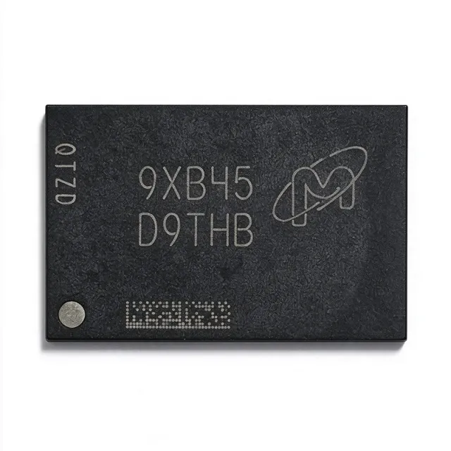
The Micron Technology MT40A512M8RH-083E is a 4Gb DDR4 SDRAM organized as 512M x 8, operating at the DDR4-2400 speed grade (1.2 GHz clock rate) and housed in a 78-ball FBGA (9 x 10.5 mm) package. It runs from a VDD/VDDQ supply of 1.2V +/-60mV with a separate VPP of 2.5V (-125mV/+250mV) and operates over 0C to +95C. A DDR4 SDRAM is a synchronous dynamic random-access memory that transfers data on both edges of the clock (double data rate), sitting within the memory hierarchy as DRAM component -> DDR SDRAM family -> main system memory. Compared with DDR3, DDR4 lowers the core supply to 1.2V, increases the internal bank count, and adds bank groups for higher effective bandwidth. The MT40A512M8RH-083E implements 8 internal banks arranged as 2 groups of 4 banks each, with an 8n-bit prefetch architecture that lets the internal array run slower while the I/O sustains 2400 MT/s. Key features include programmable data strobe preambles, on-die internal adjustable VREFDQ generation that eliminates external reference resistors, a 1.2V pseudo open-drain I/O structure that reduces I/O power, and a 64ms, 8192-cycle refresh interval for operation up to 95C. The FBGA code for this device is D9TGG, which is useful for identifying marking codes on delivered parts. The 83E speed bin corresponds to the DDR4-2400 industry speed grade with CAS latency options defined in the Micron 4Gb x4/x8/x16 DDR4 datasheet (365 pages), which should be consulted for exact tCK, CL, and tRCD timing tables. Typical applications include desktop and notebook DIMMs, embedded and industrial x86/ARM systems, networking line cards, and test equipment main memory, where a 4Gb x8 component provides a balanced capacity-per-rank and bus-width trade-off. Design considerations: DDR4 routing requires length-matched, on-end ODT-tuned fly-by topologies, and VPP must be present at power-up for the pump circuits. Verify termination (RTT_NOM/RTT_WR) settings against your memory controller's training capability. This page adds value beyond the datasheet by consolidating distributor pricing, drop-in family alternatives, application guidance, and an engineer-oriented FAQ in one place.

Запрос цены Контакты