Микросхемы памяти
Подкатегории
Товары (875)

MT48LC16M16A2BG-75 IT:D - 256Mbit SDRAM 133MHz | Micron
The Micron Technology MT48LC16M16A2BG-75 IT:D is a 256 Mbit (16M x 16) SDRAM organized as 16 mega-words by 16 bits, operating at 133 MHz (7.5 ns / -75 speed grade) in a 54-ball VFBGA (8x14) surface-mount package. The IT suffix indicates the industrial temperature grade (-40C to +85C) and the :D designator marks the die revision per Micron's SDRAM datasheet family. The device operates from a single 3.3V supply (3.0 V to 3.6 V) and is fully PC100- and PC133-compliant. An SDRAM (Synchronous Dynamic Random-Access Memory) is a type of volatile DRAM that synchronizes all operations to a system clock, enabling pipelined command execution and higher throughput than asynchronous DRAM. SDRAM sits within the memory IC hierarchy: SDRAM -> DRAM -> volatile memory -> memory IC -> semiconductor. The MT48LC16M16A2 is a member of Micron's legacy 256Mb SDRAM family (16Mx16, 32Mx8, and 64Mx4 configurations) introduced in the late 1990s and now classified as obsolete by Micron. Key features include a 133 MHz synchronous interface with all address and control signals registered on the positive clock edge, internal pipelined architecture that allows column-address changes every clock cycle, programmable CAS latency (2 or 3), burst read/write modes, and auto-refresh plus self-refresh support. The 54-VFBGA package provides a compact footprint suitable for space-constrained embedded designs, while the parallel 16-bit data bus delivers up to 266 MB/s peak bandwidth. Typical applications include legacy networking equipment, industrial control systems, point-of-sale terminals, telecommunications infrastructure, and embedded computing platforms that require reliable, high-bandwidth main memory. Designers should consult the Micron SDRAM datasheet for refresh scheduling, mode-register configuration, and PC133 timing parameters. For new designs, Micron recommends migrating to DDR/DDR2/DDR3 or newer DRAM families, as this part is in Micron's obsolete product catalog with limited long-term availability.
MT48LC16M16A2FG-75TR - 256Mbit 16Mx16 133MHz SDR SDRAM | Micron
The Micron MT48LC16M16A2FG-75TR is a 256 Mbit SDR SDRAM organized as 16M x 16 with a 133 MHz parallel interface, housed in a 54-ball VFBGA (8x14 mm) package and supplied in Tape and Reel packaging. It operates from a single 3.3V supply and is fully PC100- and PC133-compliant, with all signals registered on the positive edge of the system clock. What is an SDR SDRAM? An SDR (Single Data Rate) SDRAM is a synchronous dynamic random-access memory that transfers one data word per clock cycle, sitting one generation before DDR SDRAM in the evolution of synchronous DRAM. It belongs to the broader category of volatile memory ICs, ranking alongside SRAM and DDR/DDR2/DDR3 SDRAM, and forms part of the semiconductor memory hierarchy under the integrated circuit (IC) family. SDR SDRAM is commonly used as cost-effective main memory in legacy embedded and industrial systems where DDR is not required. Key features include a 5.4 ns access time at 133 MHz, internal pipelined 4-bank architecture, programmable CAS Latency (2/3), and self-refresh mode. The 16-bit data bus (x16 organization) gives 256 Mbit of storage with a standard LVTTL interface, while the VFBGA 54-ball package (8x14 mm) keeps the PCB footprint small for space-constrained designs. Architecturally, the device uses four internal banks that can be operated independently, allowing interleaved access for higher sustained throughput. The synchronous interface, internal pipelining, and burst-of-1, 2, 4, 8, or full-page read/write modes deliver high bandwidth with low latency for the supported 100/133 MHz clock rates. The Micron design supports auto refresh and self refresh to maintain data integrity in low-power standby modes. Typical applications include legacy industrial PCs, networking routers and switches, printers and imaging equipment, set-top boxes, and embedded computing platforms that retain an SDR SDRAM memory controller. It is also found in PC100/PC133 main-memory modules and test/measurement hardware where a known-good, mature memory interface is required. When designing with this device, ensure the PCB layout follows JEDEC trace-length and impedance rules for SSTL-2 signaling, keep VDD/VDDQ decoupling within a few millimeters of the balls, and provide proper clock-to-DQS alignment. The -75 speed grade guarantees 7.5 ns clock access time at 133 MHz, so verify tRCD and tRP against the chosen CAS Latency. This page consolidates distributor pricing, drop-in alternatives, and practical design notes that go beyond the manufacturer datasheet, helping engineers evaluate availability and second-source options for legacy SDRAM designs.

MT48LC16M16A2P-7E:D - 256Mbit SDRAM x16 133MHz 54-TSOP II | Micron
The Micron MT48LC16M16A2P-7E:D is a 256 Mbit Synchronous DRAM (SDRAM) organized as 16M words x 16 bits per word, supplied in a 54-pin TSOP II package, and qualified to the -7E speed grade for 133 MHz (PC133) operation. The :D suffix denotes the RoHS-compliant, lead-free matte-tin finish and tray packaging. It operates from a 3.3 V (3.0 V - 3.6 V) supply and presents a fully synchronous, LVTTL-compatible parallel interface with all address and data signals registered on the positive edge of the system clock. What is SDRAM? Synchronous DRAM is a generation of dynamic random-access memory whose read, write, and refresh operations are timed by a free-running system clock rather than by asynchronous control signals. SDRAM occupies a position in the memory hierarchy above asynchronous DRAM and below subsequent generations such as DDR, DDR2, and DDR3; it is the parent category that includes PC66, PC100, and PC133 variants used in late-1990s and early-2000s computing, networking, and embedded systems. Within a system-on-chip or processor board, SDRAM typically functions as the main off-chip working memory, sitting between the CPU/ASIC and any non-volatile storage. Key features of the MT48LC16M16A2P-7E:D include a 5.4 ns clock access time, an internal pipelined architecture that allows the column address to be changed every clock cycle, four internal banks for concurrent operation, programmable CAS latency (2 or 3), programmable burst length (1, 2, 4, 8, or full page), and auto-refresh plus self-refresh modes. The 16-bit data bus supports PC100 and PC133 compliance, while a deep, pipelined internal organization enables sustained throughput approaching the theoretical peak for the chosen bus width. Typical applications include industrial controllers, networking line cards, set-top boxes, printers, and legacy PC mainboards where 256 Mbit of low-cost, high-density, byte- or word-oriented working memory is required. The wide x16 data interface is convenient for color LCD frame buffers, DSP program/data stores, and 16-bit or 32-bit microprocessor external memory expansions. PC133 timing ensures compatibility with legacy host controllers and the Via/Intel chipsets of that era. When designing with this device, ensure that VDD and VDDQ are decoupled with 0.1 uF and 0.01 uF capacitors placed close to the pins, that all address/control traces are length-matched for clean clock-edge capture, and that a proper SSTL- or LVTTL-compatible clock with controlled impedance is provided. The self-refresh current should be budgeted for battery-backed or low-power standby use. This page synthesizes distributor pricing for the Micron MT48LC16M16A2P-7E:D, drop-in equivalent SDRAM candidates from Micron's own catalogue and cross-brand Alliance Memory alternatives, plus practical design notes not consolidated on any single manufacturer page.
MT48LC4M32B2B5-7G - 128Mb x32 SDRAM 143MHz | Micron
The Micron MT48LC4M32B2B5-7G is a 128 Megabit (4M x 32-bit) Synchronous DRAM (SDRAM) organized as four internal banks, operating from a 3.0 V to 3.6 V single supply and packaged in a 90-ball 8 mm x 13 mm VFBGA (Tape and Reel). It delivers a 143 MHz maximum clock rate with a 5.5 ns access time and uses a fully synchronous interface with LVTTL-compatible I/O, an internal pipelined architecture, and programmable CAS latency of 2 or 3 clocks. What is SDRAM? Synchronous DRAM is a generation of dynamic random-access memory that synchronizes all address, data, and control signals to a free-running system clock, in contrast to the asynchronous DRAM used in earlier PCs. Within the memory hierarchy, SDRAM sits above asynchronous DRAM and below Double Data Rate SDRAM (DDR), and within modern computing platforms it remains a low-cost, low-power solution for embedded graphics, networking line cards, set-top boxes, and industrial HMI where x32 bus width is convenient and DDR is unnecessary. SDRAM -> DRAM -> volatile memory -> semiconductor IC is the standard taxonomy. Key features of the MT48LC4M32B2B5-7G include auto-refresh (64 ms / 4096 rows), self-refresh mode, four-bank operation with concurrent bank precharge, and a programmable burst length of 1, 2, 4, 8, or full page with sequential or interleave burst type. The device supports LVTTL levels on all inputs and outputs, has a deep power-down mode, and provides a CKE pin for clock enable/disable and clock suspend operation, enabling fine-grained power management in battery-backed or intermittently active systems. Architecturally the part uses an internal pipelined 2n-prefetch architecture that allows the column address to change on every clock cycle, enabling fully random access. The four-bank design lets one bank be precharged while another is being accessed, which hides precharge cycles and sustains high throughput. The x32 organization maps directly to common 32-bit embedded buses such as 32-bit microcontrollers and DSPs, eliminating bus-width glue logic in many designs. Typical applications include graphics buffers in laser printers and POS terminals, frame stores in industrial cameras, SDRAM expansion for 32-bit microcontrollers (PIC32MZ, STM32, NXP i.MX external memory bus), networking line cards and DSLAM buffers, and main memory for low-cost FPGA soft-core processors such as Nios II and MicroBlaze. The wide x32 data bus makes the part especially attractive where the host is already 32 bits wide. When designing with the MT48LC4M32B2B5-7G, follow Micron TN-48-05 layout guidelines - matched-length clock, address, and command traces, a clean 3.3 V analog supply with local decoupling, Vss/VddQ noise isolation, and proper SSTL-style termination if multiple loads are present. Note that the -7G speed grade is the 143 MHz / CL3 commercial variant; the -7 IT:G variant is the industrial-temperature equivalent for -40 C to +85 C operation, and the -6A variant is the slower 166 MHz pin-compatible grade. This page synthesizes distributor pricing, drop-in speed-grade alternatives within the same Micron x32 SDRAM family, and practical PCB design notes not found in the manufacturer datasheet.

MT48LC4M32B2P-6:G - 128Mb x32 SDRAM, 167MHz, 86-TSOP II | Micron
The Micron MT48LC4M32B2P-6:G is a 128 Mbit Synchronous DRAM (SDRAM) organized as 4 Meg x 32 bits across 4 internal banks, delivered in a 86-pin TSOP II surface-mount package. Operating from a single +3.3V ±0.3V supply, it supports a clock rate of up to 167 MHz with a 5.5 ns random access time, providing a synchronous parallel interface for high-bandwidth memory subsystems. An SDRAM (Synchronous Dynamic Random Access Memory) is a volatile memory that synchronizes all address, data, and control signals to a master clock, allowing burst-oriented transfers at one word per clock cycle. SDRAM sits in the broader hierarchy: dynamic RAM -> volatile memory -> DRAM IC -> memory IC -> semiconductor. Compared with asynchronous DRAM, SDRAM enables higher throughput by overlapping bank precharge with row activation, hiding precharge cycles behind active accesses. Key features of the MT48LC4M32B2P-6:G include LVTTL-compatible inputs and outputs, programmable CAS latency of 1, 2, or 3 clocks, burst length options of 1, 2, 4, 8, or full page, and sequential or interleaved burst type. The device supports auto precharge and auto refresh, with a 64 ms refresh window distributed across 4096 refresh cycles. An internal pipelined architecture achieves the 2n-prefetch operation while allowing the column address to change on every clock cycle for fully random access. Typical applications include networking line cards, set-top box buffers, industrial control mainboards, mid-range graphics frame buffers, and embedded systems requiring high-density synchronous memory. The x32 organization reduces address-line count for wide data buses and pairs naturally with 32-bit processors and ASICs. When designing with this SDRAM, ensure VDDQ decoupling uses 0.1 µF plus 10 µF bulk capacitors placed close to the supply pins, maintain proper trace impedance for clock and DQ lines, and verify tRCD/tRP timing budgets at the chosen CAS latency. The -6 speed grade corresponds to a 167 MHz clock (6 ns clock period). This page synthesizes distributor pricing from DigiKey, drop-in alternatives from the Micron SDRAM family and cross-brand equivalents, and practical design notes not found in the manufacturer datasheet alone.

MT48LC8M16A2P-75IT - 128Mb SDRAM 8Mx16 133MHz 54-TSOP II
The Micron MT48LC8M16A2P-75IT is a 128-Mbit synchronous DRAM (SDRAM) organized as 8M x 16 bits, housed in a 54-pin TSOP II surface-mount package. The part runs from a single 3.3 V supply, delivers a 133 MHz clock rate (7.5 ns clock period, -75 speed grade), and provides a parallel LVTTL interface ideal for main-memory and frame-buffer roles. The "IT" temperature grade covers the industrial -40C to +85C range, while the "75" speed grade corresponds to a 133 MHz tCK. An SDRAM is a dynamic random-access memory synchronized to a system clock, internally divided into multiple banks that allow interleaved read/write bursts. SDRAM sits in the memory hierarchy between processor registers and bulk storage, displacing older asynchronous DRAM by adding burst-mode access, programmable CAS latency, and pipeline-friendly timing. SDRAM is the predecessor of DDR SDRAM and is now used primarily for legacy systems, industrial controllers, and cost-sensitive embedded designs where compatibility outranks raw data rate. Key features of the MT48LCM16A2P family include 4 internal banks (BA0/BA1), programmable burst lengths of 1, 2, 4, 8 or full-page, programmable CAS latency of 2 or 3, auto-refresh and self-refresh modes, and a 64 ms refresh period (8192 refresh cycles). The 16-bit data bus with two-byte DQ masking (LDQM/UDQM) simplifies 16-bit and 32-bit host connections. A 5.4 ns random access (tAC) supports high-throughput page-mode bursts. The device uses a 3.3 V CMOS process with internal VREF and clock-alignment, an on-chip delay-locked loop is NOT present (this is an SDR part, not DDR). It conforms to the JEDEC 54-TSOP II 0.400" outline. The package carries a single die routed to bond pads, then to 54 gull-wing leads on 0.8 mm pitch; the pinout follows the JEDEC 54-TSOP-II 8Mx16 standard with one additional pin reserved (NC). Typical applications include embedded industrial controllers, legacy networking line cards, point-of-sale terminals, printers, medical instrumentation, and replacement of older 128Mbit SDRAM designs. The wide industrial temperature grade suits outdoor or factory-floor deployments, and the 128Mb density matches the working memory size of older PowerPC, MIPS, ARM7/ARM9 SoCs that natively support SDRAM. When designing with this part, populate VDD and VSSQ with 0.1 uF + 10 uF decoupling placed within 5 mm of each supply pin, and tie CKE high during normal operation. PCB layout must route clocks with 50 ohm controlled impedance and keep DQs byte-grouped to maintain skew budget; unmatched traces cause burst errors at 133 MHz. This page synthesizes distributor pricing, drop-in pin-compatible alternatives, and practical design notes not found in the manufacturer datasheet alone, helping engineers select between industrial/commercial temperature grades, speed bins, and modern replacements.
MT48V8M32LFB5-8 - 256Mbit Mobile SDRAM, 125 MHz, 90-VFBGA | Micron
The Micron MT48V8M32LFB5-8 is a 256-Mbit Mobile Low-Power SDRAM (LPSDR) organized as 8M words x 32 bits, supplied in a compact 90-ball VFBGA (8x13 mm) package. Per Micron's mobile SDRAM datasheet family, the device supports a parallel interface clocked up to 125 MHz (8 ns tCK / -8 speed grade), delivering a peak data rate of 250 MT/s per I/O on a 32-bit bus and is qualified for low-power handheld and battery-backed embedded designs. What is Mobile SDRAM? Mobile SDRAM (Synchronous DRAM) is a class of low-power synchronous DRAM derived from the JEDEC SDRAM standard, designed for portable, battery-powered systems where standby current and partial-array refresh features directly determine battery life. Within the memory hierarchy, Mobile SDRAM sits between commodity SDRAM and higher-density LPDDR/LPDDR2; it provides synchronous burst access, programmable CAS latency, and partial-array self-refresh (PASR) while remaining pin-compatible with standard SDRAM controllers. Mobile SDRAMs are commonly used as the main working memory in feature phones, PDAs, portable media players, GPS receivers, and industrial handhelds that need SDRAM-like bandwidth but cannot tolerate the higher standby current of conventional SDRAM. Key features of the MT48V8M32LFB5-8 include 256 Mbit density (8M x 32), internal banks organized for high-throughput burst access, and selectable PASR modes that let the system retain only a portion of the array in self-refresh, dramatically cutting standby current. The device supports standard SDRAM commands (MR, REF, ACT, PRE, READ, WRITE) with programmable CAS latency and burst length, simplifying integration with general-purpose SDRAM controllers and embedded MPUs that lack native LPDDR support. Operating from a single 3.3 V supply (Vdd/Vddq), the device is targeted at mobile platforms where 1.8 V LPDDR is unnecessary but extended battery life is required. Architecturally, the device uses a 4-bank internal structure with synchronous pipelined access and on-chip refresh, packaged in a fine-pitch 90-ball VFBGA measuring 8 mm x 13 mm. This small form factor makes the part suitable for space-constrained portable products while the x32 organization reduces chip-enable count on the host bus. According to Micron's mobile SDRAM datasheet, the -8 speed grade corresponds to a 125 MHz clock and 7 ns access time at CAS latency 3. Typical applications include handheld GPS terminals, portable medical data loggers, feature-phone baseband subsystems, industrial barcode scanners, and ruggedized handheld terminals that pair a low-power application processor with a 32-bit SDRAM interface. The wide-word organization is convenient for processors with 32-bit external memory buses, removing the need for two x16 devices in parallel. When designing in this part, follow the VFBGA PCB layout guidelines in Micron's TN-00-08 application note: route the clock net with controlled impedance, match DQ/DQS trace lengths within a tight skew budget, and provide solid ground planes beneath the BGA to suppress simultaneous switching noise. Decoupling must include a 0.1 uF ceramic capacitor per Vdd/Vddq pin pair placed as close as physically possible to the package balls. This page synthesizes distributor pricing, pin-compatible alternatives, and practical design notes not found in the manufacturer datasheet, providing an independent reference for engineers selecting Mobile SDRAM for low-power embedded designs.

MT4LC4M16R6TG-5 - 4M x 16 EDO DRAM, 50-pin TSOP | Micron
The Micron MT4LC4M16R6TG-5 is a 4 Meg x 16 Extended Data-Out (EDO) dynamic random-access memory organized as 67,108,864 words of 16 bits each, packaged in a 50-pin TSOP (Type II) form factor and designed for a single +3.3V ±0.3V power supply. It features a -5 speed grade, indicating a 50 ns RAS access time, and uses a high-performance CMOS silicon-gate process that delivers low-power consumption suitable for extended battery-life applications. An EDO DRAM is a dynamic random-access memory variant that holds the output data valid longer than a standard Fast Page Mode DRAM by extending the column-address latch, enabling the next cycle to begin without waiting for a full precharge. EDO sits in the historical hierarchy between FPM DRAM and synchronous SDRAM, and was widely adopted in graphics frame buffers, set-top boxes, and PC peripherals before SDRAM displaced it in the late 1990s. EDO parts remain in use today in industrial, instrumentation, and legacy embedded designs where compatibility and long-term supply outweigh bandwidth. Key features include an industry-standard x16 pinout, timing, functions, and package that simplify second-sourcing; 12 row by 10 column addressing for the R6 revision; TTL-compatible inputs, outputs, and clocks; and CMOS-compatible standby current. The device supports read, write, read-write, and read-modify-write cycles, plus EDO page mode for high-bandwidth sequential access. Self-refresh and auto-refresh modes reduce system power by maintaining data without CPU intervention. Architecturally, the MT4LC4M16R6TG-5 integrates four internal memory banks that share the 16-bit data I/O, with multiplexed address inputs, /RAS, /CAS, /WE, and /OE control signals. Refresh is performed via /RAS-only refresh, /CAS-before-/RAS refresh, or hidden refresh, with a 64 ms refresh interval distributed across 4096 refresh cycles. The 50-pin TSOP-II package is optimized for surface-mount assembly on standard 0.8 mm pitch footprints. Typical applications include video frame buffers, laser-printer engines, networking line cards, industrial control panels, set-top box graphics memory, and legacy PC graphics adapters. The wide data bus and EDO page mode make the part especially effective for sequential block transfers such as pixel read/write in graphics subsystems and bit-mapped LCD controllers. The -5 speed grade suits mid-frequency microcontroller and embedded-MPU buses operating in the 25-40 MHz range. When designing with this device, ensure that the host controller generates proper EDO timing with /CAS held low through consecutive cycles and that the supply rail stays within 3.0V to 3.6V. Decouple VCC with a 0.1 µF ceramic capacitor placed within 5 mm of the VCC pin, and respect the 4096-cycle / 64 ms refresh requirement to preserve data integrity. This page synthesizes distributor pricing, drop-in alternatives, and practical design notes not found in the original Micron datasheet.
MT53B128M32D1NP-062 - 4Gbit LPDDR4 SDRAM 1.6GHz | Micron
The Micron Technology MT53B128M32D1NP-062 is a 4 Gbit Mobile LPDDR4 SDRAM organized as 128M x 32, operating at a 1.6 GHz clock frequency from a 1.1V supply, housed in a 200-ball WFBGA (10 x 14.5 mm) package. LPDDR4 (Low Power Double Data Rate 4) SDRAM is a member of the JEDEC-defined DDR SDRAM family optimized for mobile and power-sensitive embedded systems. Compared with DDR3L or DDR4, LPDDR4 achieves higher bandwidth per watt by lowering the core supply voltage to 1.1V and using a point-to-point channel architecture. In the memory hierarchy it sits under DRAM -> synchronous DRAM -> mobile SDRAM, and it is the dominant main-memory technology in smartphones, tablets, automotive infotainment, and edge AI platforms. Key features of this device include 4 Gbit density in a single 32-bit channel organization (128M x 32), 1.6 GHz operation (3200 MT/s data rate class), a low 1.1V core supply, and extended industrial or automotive temperature variants (the AUT:A grade is specified from -40C to +125C TC and qualified to AEC-Q100). The -062 speed grade defines the maximum clock frequency of the part. The WFBGA package uses a ball grid array for improved signal integrity and thermal performance relative to wire-bonded alternatives. Technically, the MT53B128M32D1NP family integrates Micron's LPDDR4 core with bank-group architecture, enabling fast random row access and efficient burst interleaving. Low-power features such as partial-array self-refresh, deep power-down, and per-bank refresh reduce standby current, which directly extends battery life in portable designs. The 32-bit single-die organization simplifies controller mapping for mid-density systems that do not require a full 64-bit dual-die configuration. Typical applications include automotive infotainment and instrument cluster memory, industrial human-machine interfaces, edge AI accelerators, networking line cards, and embedded vision systems where 4 Gbit of bandwidth-efficient DRAM is sufficient. When designing with this device, ensure your memory controller supports the JEDEC LPDDR4 protocol, and account for trace-length matching and termination on the high-speed data bus to meet signal-integrity requirements at 1.6 GHz operation. This page synthesizes distributor pricing, drop-in alternatives, and practical design notes not found in the manufacturer datasheet, with data verified as of 2026-09-02.
MT53D512M32D2NP-046 - 16Gbit LPDDR4 2133MHz DRAM | Micron
The Micron Technology MT53D512M32D2NP-046 is a 16Gbit Mobile LPDDR4 SDRAM memory IC organized as 512M x 32, operating at a 2.133 GHz data rate from a 1.1V core supply, housed in a 200-ball WFBGA package measuring 10 mm x 14.5 mm. LPDDR4 (Low Power Double Data Rate 4) is a JEDEC-defined class of DRAM optimized for mobile and power-sensitive embedded systems. Within the memory hierarchy, it sits below DDR4 server DIMMs in density per channel but far above them in power efficiency, using a low-voltage interface, deep power-down modes, and per-bank refresh to minimize energy per bit transferred. Key features include the high 16Gbit density in a single package, a 32-bit wide data bus that simplifies controller interfaces for application processors, and the -046 speed grade supporting 2133 MHz operation. Micron's D2NP NP (non-stack, single-die-planar) configuration offers a straightforward signal integrity profile compared with multi-die stacked alternatives. Architecturally, the device uses a standard LPDDR4 core with bank groups, burst length 8 and 16 access modes, and dynamic frequency scaling that lets the host processor reduce the clock in idle periods to cut quiescent power. The 1.1V VDD rail, combined with separate VDDQ I/O domain, allows fine-grained power management in battery-driven designs. Typical applications include mobile smartphone and tablet main memory, automotive infotainment and ADAS platforms (using the AIT/AUT automotive-grade variants), networking appliances, and industrial embedded computing where a compact footprint and low standby current matter. When designing with this device, pay careful attention to the 200-WFBGA fly-by routing topology, length-matched address/command lines, and reference voltage (VREFCA/VREFDQ) decoupling, as LPDDR4 timing budgets are tighter than DDR3L predecessors. On-die termination (ODT) settings should be validated across the full temperature range. This page synthesizes distributor pricing and availability, same-package drop-in alternatives including the MT53E LPDDR4X successor, and practical layout guidance not found in the manufacturer datasheet.

MT53E1G32D2FW-046 AUT:C - 32Gb LPDDR4X SDRAM | Micron Automotive
The Micron MT53E1G32D2FW-046 AUT:C is a 32 Gbit Mobile LPDDR4X SDRAM memory IC organized as 1G x 32, delivering a parallel data interface at 2.133 GHz clock frequency (3.5 ns access time) in a 200-ball TFBGA (10x14.5 mm) surface-mount package. The device operates from 0.6V/1.1V supplies and is AEC-Q100 qualified for automotive applications, targeting the -40C to +125C automotive grade-2 temperature range. LPDDR4X SDRAM is a low-power double data rate synchronous DRAM standard defined by JEDEC, optimized for mobile, automotive, and embedded platforms. Within the memory hierarchy, LPDDR4X sits between LPDDR4 and LPDDR5: it lowers the I/O voltage from 1.1V to 0.6V versus LPDDR4 while maintaining the same internal VDD of 1.1V, reducing dynamic power by roughly 20% at equivalent throughput. Micron's Mobile LPDDR4X family is widely deployed in automotive infotainment, ADAS controllers, and telematics modules where high density, low power, and AEC-Q100 qualification converge. Key features include a 32 Gbit density in a single die, 32-bit data width per channel, a maximum clock of 2.133 GHz (data rate 4266 MT/s), on-die temperature sensor with auto self-refresh, ZQ calibration, write leveling, auto precharge, asynchronous reset, and data mask function. The 200-TFBGA package (10 x 14.5 mm) integrates the full 32 Gbit on a single chip, eliminating the need for multi-chip packaging at this density. Typical applications include automotive infotainment head units, advanced driver-assistance systems (ADAS) controllers, digital instrument clusters, in-vehicle networking gateways, and ruggedized telematics control units. The wide operating temperature range (automotive grade 2: -40C to +105C with peak support up to +125C) and AEC-Q100 qualification make this part suitable for under-hood and outdoor-mounted automotive modules. When designing with this LPDDR4X, ensure the host SoC supports LPDDR4X (not just LPDDR4), since the 0.6V VDDQ requirement is not backward compatible. Route the high-speed command/address and DQ lanes as impedance-controlled 80-ohm differential or 40-ohm single-ended traces, with length matching within 25 mils across the byte lane.
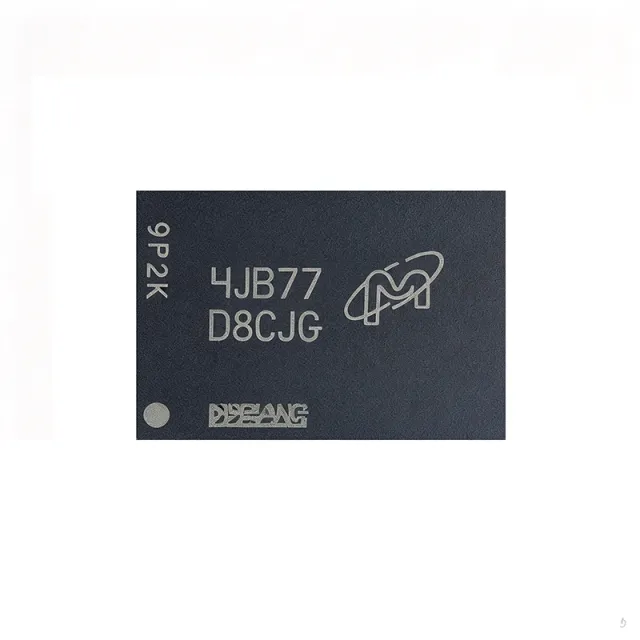
MT53E1G32D2FW-046 WT:B - 32Gb LPDDR4 SDRAM | Micron
The Micron MT53E1G32D2FW-046 WT:B is a 32 Gbit Mobile LPDDR4 SDRAM organized as 1G x 32, supplied in a 200-ball TFBGA package measuring 10 mm x 14.5 mm, and clocked at 2.133 GHz (4266 MT/s data rate) with a 3.5 ns clock access time. It supports the LPDDR4 protocol (LPDDR4X-compatible VDDQ/VDD2 combination as published by Micron) and runs from a 1.1 V/1.8 V dual-rail supply, making it a standard-density option for memory-down mobile and embedded designs. What is LPDDR4? LPDDR4 (Low Power Double Data Rate 4) is a JEDEC-standard low-power volatile memory (LPDRAM) category that evolved from DDR SDRAM with the goals of higher bandwidth per watt and lower I/O voltage. It sits in the hierarchy LPDDR4 -> LPDDR -> Mobile DRAM -> Volatile Memory -> DRAM -> Semiconductor IC. Compared with LPDDR3, LPDDR4 introduces a 16-bit-per-channel architecture, lower VDDQ (1.1 V vs 1.2 V), deeper power-down states, and command/address on-package training, all of which raise both frequency headroom and energy efficiency for smartphones, tablets, and AI edge SoCs. The MT53E1G32D2FW-046 WT:B integrates the standard LPDDR4 feature set: auto precharge, data mask, ZQ calibration, write leveling, an on-die temperature sensor, and an asynchronous reset pin. The dual-die-package (DDP) construction delivers 32 Gb (4 GB) in the 200-ball TFBGA while staying within a thin mobile-style footprint, and the -046 speed bin maps to a 2133 MHz clock with 3.5 ns tCK - this matches the JEDEC 4266 MT/s peak data rate for x32, single-channel configurations. Typical applications are 4 GB main memory in smartphones and tablets, automotive infotainment and ADAS memory-down subsystems, AI edge / inference SoC working memory, and always-on companion tiles for wearable and IoT gateways. The wide operating temperature range and AEC-Q100-ready process node also make the device a strong fit for industrial HMI and ruggedized tablets. When designing with this device, follow Micron's reference PCB layout, place the 0.1 uF + 1 uF decoupling network within 1 mm of the balls, and provide a clean 1.1 V/1.8 V rail with low ripple. Use the on-die temperature sensor output to throttle the host SoC and to drive ZQ calibration timing. This page synthesizes distributor pricing, same-package Micron speed-bin and capacity variants, cross-brand pin-to-pin equivalents, and PCB-aware design guidance not bundled in the manufacturer datasheet.
MT53E2G32D4DE-046 - 64Gbit LPDDR4X SDRAM 2133MHz | Micron
The Micron Technology MT53E2G32D4DE-046 is a 64Gbit mobile LPDDR4X SDRAM organized as 2G x 32, operating at 2133 MHz (3.5 ns cycle) in a 200-ball TFBGA package measuring 10 x 14.5 mm. As an LPDDR4X device, it uses low-VDDQ I/O (1.06 V to 1.17 V supply) to cut interface power versus standard LPDDR4. LPDDR4X (Low Power Double Data Rate 4X) is a JEDEC-defined mobile DRAM interface optimized for battery-powered and bandwidth-hungry systems. In the memory hierarchy it sits as high-density, high-speed working memory: DRAM -> synchronous DRAM -> mobile LPDRAM -> LPDDR4X, providing the main volatile working storage between the application processor and nonvolatile flash storage. Key features include the 64Gbit density in a single die, x32 I/O width, 2133 Mbps data rate per pin, auto precharge, write leveling, ZQ calibration, a built-in temperature sensor, auto self-refresh, data mask (DM) function, and an asynchronous reset input. The temperature sensor enables autonomous self-refresh rate adjustment, protecting data retention while minimizing refresh power across the operating range. Technically, the device is a high-speed CMOS dynamic random-access memory with a 16n-bank architecture and quarter-density bank grouping, transferring on both clock edges at 2.133 GHz effective. The -046 speed bin defines the 3.5 ns clock cycle. Available temperature grades include WT (-25C to +85C), AIT (-40C to +95C, industrial), and AUT (-40C to +125C, automotive), all sharing the same die and 200-ball footprint. Typical applications include AI edge accelerators, NVIDIA Jetson-class modules, automotive infotainment and ADAS domains, 5G network equipment, and industrial HMI systems requiring 8GB-class DRAM with LPDDR4X power efficiency. Design consideration: LPDDR4X fly-by routing requires per-byte write leveling and careful length matching; verify VDD2/VDDQ rail sequencing per the manufacturer datasheet power-up procedure to avoid latch-up. This page synthesizes distributor pricing, temperature-grade alternatives, cross-reference guidance, and practical design notes not consolidated in the manufacturer datasheet.
MT53E2G32D4DE-046 WT:A - 64Gb LPDDR4X SDRAM 2G×32 | Micron
The Micron MT53E2G32D4DE-046 WT:A is a 64-Gbit Mobile LPDDR4X SDRAM organized as 2G × 32 bits, housed in a 200-ball TFBGA (10 × 14.5 mm) package and specified for the -046 speed grade (2133 MHz clock / 3.5 ns tCK). It operates from a 1.06 V to 1.17 V supply and targets mobile, automotive-cockpit, and ultra-compact embedded designs where low DRAM power and high bandwidth density are critical. The part carries an operating temperature range of -25 °C to +85 °C, suiting commercial and mildly harsh environments. LPDDR4X SDRAM is the low-power double-data-rate successor to LPDDR4, designed for smartphones, tablets, AI edge inference modules, and Always-On mobile platforms. The "X" suffix denotes a reduced I/O voltage (0.6 V VDDQ versus 1.1 V in plain LPDDR4), which lowers interface power by up to ~40% at the same data rate. LPDDR4X inherits LPDDR4's 16n prefetch architecture and PoD/HSUL signaling, and Micron's MT53E family extends this lineage with higher per-die density (up to 64 Gb) and additional low-power states such as Deep Power-Down and Per-Pin VRCG. Key features of the MT53E2G32D4DE-046 WT:A include a 2133 MHz data clock (4266 MT/s effective), dual-channel / dual-rank device organization, on-die temperature sensor, programmable refresh, and a parallel command/address interface compatible with standard LPDDR4X controllers. The 200-ball TFBGA footprint supports 1.0 mm ball pitch and integrates a single die-stack package (SDP) configuration, simplifying PCB layout versus multi-die variants. Architecturally, this device uses Micron's 1y/1z-class DRAM process with internal bank-grouping of 8 banks per channel. Dual-rank operation enables higher capacity without increasing the package ball count, while the 0.6 V HSUL_12 interface reduces I/O power dramatically compared with LPDDR4. The result is a memory well suited to sustained data rates (4266 MT/s peak) while maintaining sub-1 W active power for 64-bit channel bandwidth. Typical applications include smartphone application processors, tablet main memory, AI accelerator edge inference cards (e.g. wearables, smart cameras), and automotive infotainment ECUs requiring -40 °C to +85 °C tolerances. It also fits portable gaming devices, AR/VR head-mounted display buffers, and IoT gateways with on-device AI. When designing in this part, verify controller compatibility with the 0.6 V VDDQ rail and ensure PCB trace matching for the 4266 MT/s data rate. Decoupling must be sized for LPDDR4X burst current (consult Micron TN-46 series for reference). The 200-ball TFBGA requires assembly under JEDEC J-STD-020 MSL-3 profile. This page synthesizes distributor pricing, drop-in alternatives within the MT53E family, and practical PCB / thermal guidance drawn from Micron datasheets and TN-series technical notes - information not bundled on any single distributor page.
MT53E768M64D4HJ-046 - 48Gbit LPDDR4X SDRAM | Micron
The Micron Technology MT53E768M64D4HJ-046 is a 48Gbit Mobile LPDDR4X SDRAM memory IC organized as 768M x 64, operating at 2133 MHz (2133 Mbps/pin data rate, 3.5 ns access time) with an LVSTL I/O interface, housed in a 556-ball WFBGA (12.4 mm x 12.4 mm) package. LPDDR4X (Low Power Double Data Rate 4X) is a JEDEC-defined high-bandwidth, low-voltage mobile DRAM standard used as the main-system memory in smartphones, tablets, automotive infotainment, and edge-AI compute platforms. LPDDR4X sits within the mobile DRAM hierarchy alongside LPDDR4 and below LPDDR5, and is distinguished from LPDDR4 by a lower VDDQ I/O supply that significantly reduces interface power at the same data rate. Key features of this device include its 48Gbit (6 GB) density in a single package, a wide 64-bit data bus, 2133 MHz clock rate with 3.5 ns access latency, and the ultra-compact 556-ball fine-pitch BGA (FBGA/WFBGA) footprint suited to space-constrained PCBs. Micron offers this die in multiple temperature and status suffixes (AAT, AUT, AIT, WT) covering commercial and automotive-grade operating conditions. The MT53E LPDDR4X family uses a CMOS dynamic memory core with bank-group architecture supporting burst accesses over a parallel interface, and quad-die package (QDP) variants are referenced by distributors (FBGA QDP coding on the B-suffix speed bins). Signals use LVSTL (Low Voltage Swing Terminated Logic) terminated I/O for signal integrity at 2133 Mbps/pin. Typical applications include automotive digital cockpits and ADAS platforms, high-resolution mobile displays and handsets, networking and edge-AI compute modules, and embedded systems requiring multi-gigabyte memory bandwidth in a small footprint. Design consideration: LPDDR4X routing demands strict length matching of the 64-bit data bus, on-die-termination configuration during controller initialization, and a regulated VDD2/VDDCA power rail with fast transient response; consult the Micron datasheet and controller compatibility list before layout. This page synthesizes distributor listings, temperature-suffix variants, and drop-in same-die alternatives not consolidated in the manufacturer part catalog.

MT58L64L32FT-10 - 2Mb Sync Burst SRAM 10ns 66MHz | Micron
The Micron Technology MT58L64L32FT-10 is a 2-Mbit flow-through synchronous burst SRAM organized as 64K x 32/36 (also configurable as 128K x 18), delivering a fast 10 ns clock/access time at clock rates up to 66 MHz in a 100-lead TQFP (14 x 20.1 mm) package. A synchronous burst SRAM is a static random-access memory that synchronizes address, data, and control inputs to an external clock and generates burst addresses internally, making it a key member of the memory IC family that sits within the broader semiconductor hierarchy (SRAM -> static RAM -> volatile memory -> memory IC -> integrated circuit). Unlike asynchronous SRAMs, burst-mode devices such as the MT58L64L32FT-10 prefetch sequential addresses, reducing effective access time for cache-like workloads and pipelined bus masters. Key features include single +3.3 V power supply (VDD, +0.3 V/-0.165 V tolerance), a separate isolated +2.5 V or 3.3 V output buffer supply (VDDQ) for I/O voltage flexibility, fast clock-to-output and OE# access times, individual BYTE WRITE enable controls, and SNOOZE MODE for reduced-power standby. Common data input/output pins simplify bus routing on 32-bit and 36-bit (byte-parity) systems. Architecturally, the flow-through (non-pipelined) SyncBurst design presents data on the same cycle the address is captured, eliminating pipeline latency and simplifying timing closure for controllers that expect zero-wait-state reads and writes. Registered outputs driven by the internal burst address counter support linear, interleaved, and alternate burst sequences per industry-standard processor burst orders. Typical applications include network router and switch line-card buffering, FPGA and DSP external memory expansion, telecom equipment control-plane memory, industrial controllers, and test instrumentation where deterministic 10 ns access and 66 MHz burst throughput are required. Design considerations: tie VDDQ to the host bus I/O voltage (2.5 V or 3.3 V), use SNOOZE MODE (asserting ZZ) to cut standby power during idle periods, and verify burst-order configuration straps against the host processor (linear vs. interleaved) before layout freeze. This page synthesizes distributor availability data, same-family drop-in speed/temperature variants, and practical design guidance not consolidated in the manufacturer datasheet.
MT60B2G8HB-48B:A - 2.4 GHz DDR5 16Gb 2Gx8 SDRAM | Micron
The Micron MT60B2G8HB-48B:A is a 16 Gbit DDR5 SDRAM organized as 2G x 8 (256M x 8 logical bank groups), housed in an 82-ball VFBGA (9x11) package with POD (Pseudo Open Drain) 1.1 V signaling. It operates at a 2400 MHz data clock (4800 MT/s effective), supports on-die ECC, and is qualified for the 0 to 95 °C commercial temperature range. DDR5 SDRAM represents the fifth generation of Double Data Rate synchronous DRAM and follows the JEDEC JESD79-5 standard. Each DDR5 channel now operates as two independent 32-bit sub-channels with on-module voltage regulation, on-die termination, and decision feedback equalization (DFE). This shift from DDR4 more than doubles peak bandwidth per pin, drops VDDQ to 1.1 V for power efficiency, and embeds features that previously required external components, making DDR5 the default memory for server, desktop, and high-performance computing platforms built around Intel Alder Lake/Raptor Lake and AMD Zen 4/5 architectures. Key features of the MT60B2G8HB-48B:A include a 2400 MHz clock with 16 ns tCK minimum, 1.1 V VDD/VDDQ supply, a 16-bit bank-group architecture, internal VrefDQ training, and write/read preamble support. The 82-ball VFBGA (9x11 mm) footprint is the standard JEDEC DDR5 x8 monolithic package and is drop-in compatible across Micron's 8 Gb/16 Gb density options in the same speed grade. Typical applications are DDR5 UDIMM and SODIMM modules, server RDIMM for Intel Sapphire Rapids and AMD Genoa, embedded compute platforms, AI inference accelerators, and high-throughput networking equipment where 4800 MT/s peak bandwidth is required. Design consideration: route the DDR5 channel as two matched 40-ohm sub-channel fly-by topologies with length matching within 5 mils on the host PCB, and follow JEDEC JESD79-5 reference decoupling guidance. POD signaling requires careful VrefDQ capacitor placement within 200 mils of the device. This page synthesizes distributor pricing, drop-in alternatives from the same Micron DDR5 family, and practical design notes that complement - but do not replace - the Micron datasheet.

MT60B2G8RZ-64B-IT-H - 16Gb DDR5 SDRAM 3.2 GHz 78-FBGA | Micron
The Micron MT60B2G8RZ-64B-IT-H is a 16 Gbit DDR5 SDRAM memory IC organized as 2G × 8, operating at up to 3.2 GHz data rate in a 78-ball Fine-pitch Ball Grid Array (FBGA) measuring 7.5 mm × 11 mm, in industrial temperature grade (IT). It is a JEDEC-compliant DDR5 SDRAM component designed for high-bandwidth, low-voltage memory subsystems in mainstream server, client, and embedded platforms. What is a DDR5 SDRAM? DDR5 (Double Data Rate 5) Synchronous DRAM is the fifth generation of DDR memory, succeeding DDR4. Compared with DDR4, DDR5 doubles the peak data rate (starting at 3200 MT/s with on-die termination and decision feedback equalization), halves the channel voltage (1.1 V VDD, 1.1 V VDDQ), introduces on-die ECC, and doubles bank group counts to improve parallelism. In the broader taxonomy: DRAM -> volatile memory -> semiconductor memory -> integrated circuit. The MT60B2G8RZ-64B-IT-H therefore sits in the volatile main-memory tier of any computing platform. Key features include a maximum operating supply current of 363 mA, an industrial operating temperature range of 0 °C to +95 °C, a 1.1 V nominal supply (VDD/VDDQ), on-die termination (ODT), and a 78-ball FBGA package that supports high-speed signaling at 3200 MT/s. The 7.5 mm × 11 mm outline is shared across Micron's 16 Gb DDR5 ×8 family, enabling drop-in compatibility across density, speed, and temperature grades. The device uses a fly-by topology for command, address, control, and clock signals, and integrates an on-DIMM voltage regulator (PMIC interface) for client DIMM-style deployments. Decision Feedback Equalization (DFE) and Write Leveling maintain signal integrity at 3200 MT/s, while the 16n prefetch and bank-group architecture double the effective page size compared to DDR4. Typical applications include DDR5 UDIMM and SODIMM modules for desktop and notebook platforms, embedded computing platforms requiring industrial-grade memory, single-board computers (SBC) and edge AI accelerators, networking line cards with high packet buffer demand, and entry-level server memory modules. The IT grade makes it suitable for harsher thermal envelopes than commercial-grade DRAM. When designing with this part, follow JEDEC JESD79-5 PCB layout and routing rules for DDR5: keep the byte-group DQ/DQS lengths matched within 5 mil, maintain a 100 Ω differential impedance on DQ/DQS pairs, and use a reference termination scheme compliant with the host memory controller's RTT selections. The DRAM does not require an external PMIC on the component itself but expects a 1.1 V rail in system designs. This page synthesizes distributor pricing, same-family drop-in alternatives, and practical design notes not found in the manufacturer datasheet, all verified as of 2026-10-05.

MT62F1536M32D4DS-023 - 48Gbit LPDDR5X SDRAM | Micron Technology
The Micron Technology MT62F1536M32D4DS-023 is a 48Gbit Mobile LPDDR5X SDRAM memory IC organized as 1.5G x 32, operating at up to 4.266 GHz with LVSTL (Low Voltage Swing Terminated Logic) interface signaling, supplied in a 315-ball TFBGA (12.4 mm x 15 mm) surface-mount package. LPDDR5X (Low Power Double Data Rate 5X) is the extended-speed evolution of the LPDDR5 DRAM standard defined by JEDEC, engineered for mobile and power-constrained computing. As a volatile SDRAM within the broader memory hierarchy (DRAM -> mobile DRAM -> LPDRAM), it stores working data for application processors while minimizing power per bit transferred, making it the dominant main-memory technology in smartphones, tablets, and AI edge devices. Key features of this component include the 48 Gbit (6 GB) density in a single package, the 1.5G x 32 organization that supports wide 32-bit memory channels, and the LPDDR5X speed grade supporting a 4.266 GHz clock rate - a substantial bandwidth uplift over LPDDR5 (3.2 GHz, as seen in the related WT:B variant). The LVSTL interface reduces I/O swing to lower simultaneous-switching noise and I/O power at multi-gigahertz data rates. The device operates from a supply voltage of 1.01 V to 1.12 V (VDDQ domain), reflecting the reduced core and I/O voltages that define the LPDDR5X generation. The 315-TFBGA package (12.4 x 15 mm) uses a fine-pitch ball grid array to accommodate the high ball count required by the 32-bit data bus, address/control, and power delivery - a footprint intended for HDI (high-density interconnect) mobile-class PCB stackups. Typical applications include flagship smartphone main memory, AI accelerator and edge-inference modules that stream large weight arrays, automotive infotainment and ADAS domains (the AEC-Q100-qualified AUT:C variant of this same die serves that market), and high-performance portable compute such as tablets and XR headsets. High bandwidth at low power per gigabyte is the common requirement across all of these. Design consideration: LPDDR5X signal integrity demands strict length matching of the data groups, careful controller training for read/write eye margins, and following the power-rail sequencing and termination guidance in the manufacturer datasheet; reuse a validated reference layout rather than improvising the fly-by topology. This page synthesizes distributor pricing and availability, drop-in same-die variant comparisons (WT, AUT, AAT, AIT speed/temperature options), and practical design notes not found in the manufacturer datasheet.
MT62F1G32D2DS-026 WT:C - 32Gb LPDDR5 SDRAM 3.2GHz 315-TFBGA | Micron
The Micron MT62F1G32D2DS-026 WT:C is a 32 Gbit Mobile LPDDR5 SDRAM memory IC organized as 1G x 32 bits, operating at a 3.2 GHz parallel clock and housed in a 315-ball TFBGA (12.4 x 15 mm) surface-mount package. According to Micron's LPDDR5 part catalog, this device is qualified for the JEDEC LPDDR5 standard and targets power-constrained mobile platforms. LPDDR5 (Low-Power Double Data Rate 5) is the fifth generation of JEDEC-standardized low-power DRAM, succeeding LPDDR4/LPDDR4X. As a Mobile SDRAM, it belongs to the hierarchy volatile memory -> DRAM -> SDRAM -> Mobile SDRAM -> LPDDR5, and is engineered for applications where both high bandwidth and very low standby power are mandatory. LPDDR5 introduces per-channel decision feedback equalization (DFE), data-copy and write-X features that reduce SoC-to-DRAM traffic, and a deep sleep mode that cuts refresh current. The MT62F1G32D2DS is a dual-channel (32-bit I/O width) part aimed at flagship smartphone APs, AI edge accelerators, and thin-and-light notebooks. Key features include a 32 Gbit density (8 banks per channel × 2 channels), a 3.2 GHz data-rate clock (6400 MT/s per pin in the -026 speed grade), 1.05 V typical VDD supply voltage, and 0.9 V/1.2 V selectable VDDQ. The device supports on-die ECC for single-bit error correction in automotive and industrial workloads, and integrates a temperature-compensated refresh engine. The -026 speed bin corresponds to a 3.2 Gb/s/pin transfer rate in this part numbering scheme. The MT62F1G32D2DS-026 WT:C uses a 315-ball TFBGA package with a 0.5/0.8 mm pitch, optimized for high-density mobile PCB layouts. Two 16-bit channels share the package balls, with dedicated clock, command, and data byte lanes per channel. The package's 12.4 x 15 mm footprint and 1.0 mm max height make it compatible with smartphone motherboard stack-ups that include the application processor, the PMIC, and a discrete Wi-Fi/Bluetooth module on the same PCB. Typical applications include flagship smartphones and tablets, ultra-thin notebooks, AR/VR headsets, AI edge inference modules, automotive infotainment platforms, and 5G mmWave modem sub-assemblies. This MT62F1G32D2DS-026 WT:C variant (commercial temperature range, WT designator) is the mainstream consumer-grade SKU, while the WT:B and WT:A suffix variants target industrial/automotive-grade qualification. When designing with this part, ensure the SoC's LPDDR5 PHY supports the 6400 MT/s data rate and the 32-bit dual-channel configuration. The PCB layout must match Micron's reference 4-layer or 6-layer stack-up to keep the channel loss under 6 dB at 3.2 GHz; use 100 ohm differential impedance for the clock pair and CA/CS signals. Decoupling must follow Micron's Mobile LPDDR5 PCB design guide.

MT62F512M64D4EK-031 AIT:B - 32Gb LPDDR5 SDRAM 512Mx64 3.2GHz | Micron
The Micron MT62F512M64D4EK-031 AIT:B is a 32 Gbit Mobile LPDDR5 SDRAM organized as 512M x 64 in a 441-TFBGA (14x14) surface-mount package, operating up to 3.2 GHz with a maximum per-channel bandwidth of 12.8 GB/s. It is qualified to AEC-Q100 standards and ships in an industrial temperature grade suitable for harsh-environment automotive and embedded platforms. An LPDDR5 SDRAM is a fifth-generation low-power double data rate synchronous DRAM designed for mobile and power-constrained systems. LPDDR5 improves on LPDDR4X by introducing multi-clock command/address inputs, deeper prefetch (16n-bit or 32n-bit), higher per-pin bandwidth via CKR (Clock Request) support, and on-die error correction code (ECC). LPDDR5 sits within the SDRAM family -> DRAM -> volatile memory -> integrated circuit taxonomy, and is the dominant low-power main memory in smartphones, automotive infotainment, AI edge accelerators, and always-on embedded SoCs. Key features of the MT62F512M64D4EK-031 AIT:B include a 4 KB page size with 8-bank mode (or 2 KB page with 16-bank / bank group mode), ZQ calibration, on-chip ECC, asynchronous reset, data mask function, and optional CKR support. Differential command clock (CK_t/CK_c) and data clock (WCK_t/WCK_c) signaling improve signal integrity at high data rates. The QDP (Quad Die Package) configuration stacks four 8 Gb dies to reach 32 Gb density. Architecturally the device uses a 16n prefetch datapath feeding four 8 Gb LPDDR5 dies in a single 441-ball TFBGA, providing x64 channel width across two channels. The 031 speed bin denotes 6400 MT/s operation per pin, achieving the 12.8 GB/s peak per-channel bandwidth figure quoted by Micron. Typical applications include automotive ADAS compute platforms, in-vehicle infotainment (IVI), AI edge inference modules, premium smartphone application processors, and ruggedized industrial tablets. Designers choose this part for its AEC-Q100 qualification, large 32 Gb density, and the high bandwidth density per watt that LPDDR5 delivers versus LPDDR4X. When designing in this device, allocate adequate PCB area for the 14 mm x 14 mm BGA and route the differential CK/WCK pairs with length matching within the JEDEC LPDDR5 skew tolerance. Use Micron's reference PCB design guide for impedance and decoupling. This page synthesizes distributor pricing, drop-in alternatives, and practical design notes not found in the manufacturer datasheet.

MT62F6G24D156A-001 - 96Gbit Mobile LPDDR5 SDRAM | Micron
The Micron MT62F6G24D156A-001 is a high-density Mobile LPDDR5 SDRAM memory IC in the Micron LPDDR5 family. Decoding the Micron naming convention, the device integrates 96 Gbit of storage in a 563-ball fine-pitch BGA package, organized across multiple die stacks to deliver the bandwidth required by advanced mobile, automotive, and edge-AI platforms. A Mobile LPDDR5 (Low-Power Double Data Rate 5) SDRAM is a JEDEC-standard volatile memory that operates at low voltage (typically 1.05–1.1 V VDD and 0.9–1.0 V VDDQ) while delivering high data rates through a 16n prefetch architecture and double-data-rate I/O. LPDDR5 sits above LPDDR4X in the low-power DRAM taxonomy, trading slightly higher complexity for substantially higher bandwidth per pin and improved refresh management. It belongs to the wider class of synchronous DRAM, which itself is a subset of volatile memory ICs used as main system memory in compute platforms. Key features of the MT62F6G24D156A-001 family include high per-pin data rates (up to 6400 MT/s in LPDDR5X-class extensions), deep command/address scrambling for link robustness, on-die ECC for soft-error mitigation, and per-byte VDDQ voltage scaling that minimizes platform power. The device supports both single-rank and multi-rank channel topologies, and the 563-ball BGA exposes a wide 64-bit data interface (x64) for parallel data transfer at multi-GHz effective rates. The MT62F6G24D156A-001 is built on Micron's advanced 1y/1z-class DRAM process with Through-Silicon-Via (TSV) or wire-bond multi-die stacking in a single package, which yields a small PCB footprint relative to its capacity. The 563-ball BGA integrates ground/VDD/VDDQ decoupling balls, command/address balls, and the data DQ/DQS balls. This architecture is engineered for sustained high-bandwidth operation while keeping DRAM-array refresh current low — critical for always-on and thermally constrained platforms. Typical applications include high-end smartphone main memory, automotive infotainment and ADAS platforms, AI PC and edge inference accelerators, and 5G mmWave baseband subsystems. The combination of high density (96 Gbit), wide x64 channel width, and LPDDR5 power efficiency makes it particularly suited to designs that require multi-gigabyte system memory in a thermally constrained enclosure. When designing with this device, follow the Micron LPDDR5/LPDDR5X reference PCB layout for the 563-ball BGA: matched-length routing on the data byte lanes, proper VDD/VDDQ decoupling, and tight skew control on CK_t/CK_c. Confirm thermal headroom under sustained write workloads, as multi-gigabyte transfers at 6400 MT/s can push junction temperature above the commercial-grade limit if airflow is limited. This page synthesizes distributor pricing, drop-in alternatives, and practical design notes that complement the official Micron datasheet and PCB-layout application notes.
MT65B12G16080A00QG-92:A - 24GB HBM3E 2.3GHz X1088 WFPGA | Micron
The Micron MT65B12G16080A00QG-92:A is a 24 GB HBM3E (High Bandwidth Memory 3E) stacked DRAM device organized as X1088 with a 2.3 GHz data-rate specification, supplied in a WFPGA package. It is the latest generation of Micron's HBM family targeted at AI accelerators, GPU compute dies, and high-performance computing SoCs that require terabyte-per-second aggregate bandwidth from a compact, vertically stacked memory sub-system. HBM (High Bandwidth Memory) is a JEDEC-standardized 3D-stacked DRAM architecture that places multiple DRAM dies atop a base logic die through TSV (Through-Silicon Via) interconnects. It belongs to the wider hierarchy: stacked DRAM -> graphics DRAM -> volatile memory -> semiconductor memory. Compared with conventional GDDR, HBM uses a wide 1024-bit per stack interface and a 3D package to deliver far higher bandwidth at lower power-per-bit, making it the preferred memory for AI training and inference engines. Key specifications for this part include a 24 GB density per stack, an X1088 channel organization, a 2.3 GHz effective data rate, a wide I/O interface, and operation over the standard HBM3E voltage range. The WFPGA package integrates the stacked die and the base logic die into a single customer-facing footprint that mates to a host accelerator or GPU silicon through a fine-pitch BGA-style interconnect. Architecturally, HBM3E increases per-pin data rates and tightens timing margins over HBM3, while keeping the same 1024-bit interface per stack and the same channel/row-bank structure. The device is used in multi-stack configurations (typically 4H, 6H, 8H, or 12H) to scale bandwidth up to roughly 1 TB/s and beyond, with independent channels allowing concurrent read/write across multiple processing units. Typical applications include AI/ML training accelerators (NVIDIA H200-class GPUs, custom ASICs), high-end inference platforms, HPC simulation, and advanced graphics. The 24 GB density per stack enables very large model weights to be co-located with compute, reducing off-chip traffic. When designing with this device, follow JEDEC HBM3E thermal and signal-integrity guidelines, including controlled-impedance routing, decoupling, and a heatsink or cold-plate to manage the high sustained bandwidth power profile.
MT8LSDT1664AG10E - 128MB PC100 SDRAM DIMM | Micron
The Micron MT8LSDT1664AG10E is a 128 MB (16 Meg x 64) unbuffered 168-pin SDRAM Dual In-Line Memory Module (DIMM) organized as 16M x 64 in the PC100/PC133 JEDEC-standard form factor. It operates from a single +3.3V ±0.3V power supply and uses fully synchronous SDRAM components clocked at 125 MHz (PC100) and 133 MHz (PC133), delivering the bandwidth and latency required by late-1990s desktop systems, Pentium III/early Athlon motherboards, and legacy industrial SBCs. A SDRAM (Synchronous Dynamic Random-Access Memory) module is a type of volatile memory that synchronizes data transfers with the system clock, allowing burst-mode reads and writes at one operation per clock cycle. SDRAM DIMMs sit at the base of the PC memory hierarchy (registers/cache → DRAM → storage), and unbuffered (UDIMM) variants like the MT8LSDT1664AG10E are intended for desktops and workstations where the chipset drives the address/command bus directly without a register buffer. This Micron part is part of the legacy MT8LSDT1664A/MT16LSDT3264A DIMM family that defined the PC100/PC133 era. Key features of the MT8LSDT1664AG10E include a 6 ns access time (the "-10E" speed grade), CL2 CAS Latency support at 100 MHz, gold edge-finger contacts (the "G" suffix), operation from 0°C to +70°C (commercial temperature range), fully synchronous operation with all signals referenced to the rising clock edge, and JEDEC-standard pinout that allows drop-in replacement across compliant 168-pin UDIMM sockets. The 168-pin DIMM format uses a 64-bit data bus without ECC, which matches the bandwidth requirements of the Intel 440BX, VIA Apollo Pro, and SiS 630/633 chipset families. Typical applications for the MT8LSDT1664AG10E include legacy desktop PC memory upgrades, industrial single-board computer main memory, factory-floor PC/104 systems, test-and-measurement instrumentation that requires PC-compatible memory, refurbished legacy server base memory, and older point-of-sale terminals. The unbuffered, non-ECC organization makes it unsuitable for registered ECC server platforms; for those systems, the MT9LSDT1672AG (registered, ECC) variant is the recommended replacement. When designing or servicing with this module, observe the JEDEC initialization sequence: hold CKE low, apply stable VDD/VDDQ simultaneously, wait 100 µs, then issue a PRECHARGE-ALL and two AUTO-REFRESH commands before normal operation. Mixed-speed modules in the same bank may force the system to the slowest CAS latency, so populate banks with matched speed grades where possible. The module has reached end-of-life from Micron and is now sourced primarily through the secondary/aftermarket channel. For procurement, verify the full Micron datasheet and confirm the exact speed grade (-10E = 6 ns / 100 MHz CL2) and the gold-finger ("G") contact option. Note that the MT8LSDT1664AG10EE1 variant adds an additional testing/qualification suffix; the -10E base part is the canonical PC100 128 MB reference. This page synthesizes distributor availability, drop-in alternatives, and practical legacy-DIMM design notes not found in the standalone manufacturer datasheet.