Микросхемы памяти
Подкатегории
Товары (875)

N25Q128A13E12A0F - 128Mb SPI NOR Flash, 108 MHz | Micron
The Micron N25Q128A13E12A0F is a 128-Mbit (16M x 8-bit) multiple I/O serial NOR flash memory operating at 3V (2.7V to 3.6V), with a 108 MHz SPI bus interface and 7 ns access time, housed in a 24-ball TBGA (T-PBGA, 6x8 mm) package supplied in tape and reel. Serial NOR flash is a nonvolatile memory technology that stores code and data while allowing direct, addressable random access over the SPI bus. It occupies the memory hierarchy between parallel NOR flash (faster but pin-hungry) and SPI NAND (cheaper but block-oriented). In embedded systems, serial NOR is the standard boot medium for microcontrollers, SoCs, and FPGAs, where execute-in-place (XiP) capability lets the processor run code directly from the flash without copying it to RAM. Key features of the N25Q128A13E12A0F include single, dual, and quad SPI operation (up to 4-bit wide data transfer), 4-Kbyte subsector erase granularity on boot sectors for fine-grained parameter storage, and XiP enabled operation. The 108 MHz clock rate with quad I/O delivers effective read throughput approaching 432 Mbit/s, minimizing boot latency in XiP systems. Technically, this device belongs to Micron's N25Q (formerly Numonyx) family of 3V multiple-I/O serial flash memories, which inherits the SPI command set popularized by earlier generations and adds extended address options, deep power-down modes, and advanced sector protection. The part is specified from -40C to +125C and is offered in automotive-qualified flows per distributor listings citing AEC-Q100. Typical applications include FPGA configuration storage, embedded processor boot code, automotive infotainment and telematics modules, and networking equipment firmware storage. The 128Mb density comfortably hosts U-Boot, Linux kernel images, or large FPGA bitstreams. A key design consideration: quad-SPI signal integrity requires short, length-matched traces with series termination at 108 MHz; verify hold-time requirements when using a low-speed SPI clock for initial FPGA configuration. This page synthesizes distributor pricing, drop-in family alternatives, and practical design notes not found in the manufacturer datasheet.

N25Q128A13ESEA0F - 128Mb 3V SPI NOR Flash, SOP-8 | Micron
The Micron Technology N25Q128A13ESEA0F is a 128Mb (16MB) 3V Multiple I/O Serial NOR Flash memory with 4KB sector erase capability, housed in an 8-terminal SOP (SOIC-8 footprint) plastic package. It operates from a 2.7V to 3.6V supply over an industrial -40C to +85C temperature range. Serial NOR Flash is a nonvolatile memory category that stores code and data and executes in place (XIP), sitting within the memory IC hierarchy: serial NOR flash -> NOR flash -> flash memory -> nonvolatile semiconductor memory. Unlike NAND flash, NOR flash offers random byte-level access and high read reliability, making it the standard boot-memory technology for embedded processors and microcontrollers. Key features include 128Mb density organized as 16M x 8, multiple I/O operation (standard SPI, Dual SPI 2x I/O, and Quad SPI 4x I/O) that scales read bandwidth without changing packages, and 4KB subsector erase granularity for efficient parameter storage. The 3V supply family supports fast clocked reads essential for XIP code execution. Architecturally, the device uses Micron's pulse-trained command set with dedicated instructions for page program, sector erase, chip erase, and status polling, and supports quad I/O commands that transfer four bits per clock cycle to accelerate boot and code-fetch workloads. Typical applications include BIOS/UEFI code storage on x86 platforms, boot flash for embedded ARM and network processors, firmware storage in industrial control systems, and automotive electronics modules, where XIP execution and long-term data retention are required. Design consideration: verify that your host controller supports the N25Q command set (Micron pulse protocol) or enable the Spansion-compatible extended command set; also budget erase times for 4KB subsector operations in firmware update routines. This page synthesizes distributor pricing, drop-in alternatives including the Winbond W25Q128JVSJQTR cross-reference, and practical design notes not found in the manufacturer datasheet.

N25Q128A13ESF40G - 128Mb SPI NOR Flash, 108 MHz, SO-16
The Micron N25Q128A13ESF40G is a 128-Mbit (16 MB) serial NOR flash memory built on 65 nm NOR technology and packaged in a 16-pin SO (208 mil, SOIC-16) form factor. It operates from a 2.7 V to 3.6 V single supply and exposes the storage as 128 Mbit / 64 Mbit / 32 Mbit configurable as 1-bit, 2-bit (Dual SPI), or 4-bit (Quad SPI) per instruction, with a 108 MHz SPI-compatible bus interface and execute-in-place (XiP) capability for direct code execution from flash. A NOR flash is a non-volatile memory that supports random byte-level read access and byte-level program/erase, in contrast to NAND flash which is read in large pages. Serial NOR flash devices such as the N25Q128A13ESF40G connect over a low-pin-count SPI bus, dramatically simplifying board routing while preserving the byte-addressable random read that makes NOR ideal for code storage. Within the memory hierarchy, N25Q128A13ESF40G sits between external boot ROM and the MCU/MPU's internal SRAM, providing firmware storage that the host CPU executes in-place via XiP. Key features include a 108 MHz SPI clock with Dual/Quad I/O instruction extensions, 4 KB sub-sector erase granularity, advanced write protection with top/bottom block lock and OTP security area, 100k program/erase cycles endurance per sector, and 20-year data retention. The device also supports single 1.7 V internal core voltage operation from a single 3 V external rail. 128 Mb density provides ample space for bootloaders, OS images, and configuration data in space-constrained designs. Typical applications include firmware boot storage for STM32/i.MX RT/micro:bit-class MCUs, asset tracking and IoT edge nodes, automotive infotainment boot partitions, industrial PLC firmware storage, and consumer electronics such as set-top boxes, printers, and Wi-Fi modules. The 16-pin SOIC-16 wide-body (208 mil) package is hand-solderable and inspectable, well suited for production and rework. Designers should note that the 'F' suffix in 'ESF40G' indicates 108 MHz Quad SPI performance with a 4-second erase / 108 MHz Quad SPI mode; the 'G' suffix indicates lead-free / Pb-free / RoHS-compliant terminal finish. When migrating from parallel NOR to this part, recalculate access latencies since SPI throughput is lower per pin but Quad SPI closes much of the gap. Always honor the maximum 108 MHz SPI clock and respect tVSL/Vcc ramp requirements during power-up.
N25Q128A13ESF40G-TR - 128Mb Serial NOR Flash, 108MHz SPI, SOIC-16 | Micron
The Micron N25Q128A13ESF40G-TR is a 128-Mbit (16-Mbyte) serial NOR Flash memory built on a 65nm NOR process, supporting 1, 2, and 4-bit multi-I/O SPI operation at a maximum clock frequency of 108 MHz. It is offered in a 16-pin SOIC (SO) wide-body package and supports a single 3.0V (2.7V-3.6V) supply rail for both core and I/O. The "-TR" suffix designates the tape-and-reel packaging option for high-volume SMT assembly, while the F40 speed grade enables the 108 MHz multi-I/O read throughput. The device delivers execute-in-place (XiP) capability, advanced write protection, and a 4-Kbyte subsector erase granularity, making it a flexible code-storage and data-logging solution on space-constrained boards. A serial NOR flash is a non-volatile memory device that uses a low-pin-count synchronous serial interface (SPI) rather than a wide parallel bus. In the broader memory hierarchy, NOR flash sits at the same tier as parallel NOR for code storage but trades bus width for footprint savings; serial NOR is the dominant choice on modern microcontrollers and SoCs that lack an external memory bus. The N25Q128 family implements the JEDEC-standard Serial Peripheral Interface with extensions for Dual SPI and Quad SPI, plus an optional serial command subset for JEDEC xSPI-compatible reads. Key features include 128-Mbit density in 1/2/4-bit modes, 4-Kbyte uniform subsectors with 64-Kbyte sectors and 256-byte page programming buffer, top or bottom boot-block configuration, and security enhancements including one-time-programmable (OTP) protection, 3x 256-byte security registers, and a 64-bit unique ID. Program/erase endurance is rated at 100K cycles per sector minimum with 20-year data retention. The Quad SPI interface enables effective throughput up to 432 Mbit/s when all four I/O lines are active, comfortably supporting XiP code execution from flash on mid-range ARM Cortex-M and RISC-V SoCs. Typical applications include firmware storage for IoT gateways, asset-tracking modules, and industrial controllers; data logging in metering and predictive-maintenance systems; boot ROM plus user-data storage in FPGA-based designs; and BIOS/UEFI storage on SBCs and embedded boards. The wide SOIC-16 footprint suits hand-soldered prototypes as well as high-volume SMT lines. When designing with the N25Q128A13ESF40G-TR, observe the 108 MHz VCC/IO decoupling requirement by placing a 0.1 uF ceramic capacitor adjacent to pins 8 (VCC) and 16 (VSS). Quad SPI traces should be length-matched within approximately 25 mm to preserve sampling margin at 108 MHz, and a pull-up on the HOLD#/RESET# pin prevents unintended resets during power-rail ramp. The standard SPI command set is JEDEC-compatible, so most MCU HAL drivers work without modification. This page synthesizes distributor pricing, drop-in alternatives, and design notes not found on standalone datasheet mirrors. Pricing was captured from authorized distributors as of 2026-10-05; all pinout and timing references should be reconfirmed against the manufacturer datasheet before PCB release.

N25Q512A13GSFA0F - 512Mb SPI NOR Flash 108MHz | Micron
The Micron Technology N25Q512A13GSFA0F is a 512Mb (64MB) multiple I/O serial NOR flash memory with an SPI-compatible bus interface supporting up to 108 MHz clock in single transfer rate (STR) mode and 54 MHz in double transfer rate (DTR) mode, housed in a 16-pin SOIC (SOP-II 16/16) surface-mount package. Serial NOR flash is a non-volatile memory technology that stores code and data while retaining contents without power. Within the memory hierarchy it sits as the boot and code-storage device in embedded systems, feeding instructions to MCUs, SoCs, FPGAs, and networking processors. The SPI (Serial Peripheral Interface) bus reduces pin count and board area compared to parallel NOR, while multiple I/O (Single, Dual, Quad) and DTR modes multiply effective bandwidth. Key features of the N25Q512A13GSFA0F include 512Mb density organized as 512M/256M/128M x 1/2/4-bit, a 2.7V to 3.6V single supply voltage, 4KB sector erase granularity for efficient code updates, and an operating temperature range of -40C to +125C suitable for automotive and industrial environments. The device is constructed as a stacked pair of two 256Mb die. Architecturally, the device supports Standard, Dual Output, Dual I/O, Quad Output, Quad I/O, and DTR protocols, achieving a 7ns access performance class at full clock speed. Enhanced features such as subsector erase and execute-in-place (XIP) support allow direct code execution from the flash array. Typical applications include automotive infotainment and ADAS boot code storage, networking equipment configuration memory, and industrial FPGA/MCU firmware storage where high density and -40C to +125C operation are required. Design consideration: manage the 4KB sector erase latency in firmware by pre-erasing blocks during idle time; also verify signal integrity on SCK at 108 MHz with proper series termination and short traces. This page synthesizes distributor pricing, drop-in alternatives, and practical design notes not found in the manufacturer datasheet.
N25Q512A83G12A0F - 512Mbit SPI NOR Flash 108MHz | Micron
The Micron Technology N25Q512A83G12A0F is a 512 Mbit (64 MB) serial NOR flash memory with 128M x4 organization, a 108 MHz SPI clock rate, and a 24-ball T-PBGA (6x8 mm) package. It operates from a single 2.7 V to 3.6 V supply and supports standard, dual, and quad SPI protocols for high-throughput code storage. Serial NOR flash is a nonvolatile memory category within the broader voltage-based solid-state storage hierarchy (flash memory -> NOR flash -> serial NOR flash -> SPI memory IC). Unlike parallel NOR devices that use many address and data lines, serial NOR devices communicate over a compact SPI bus of 4 to 6 signals, trading absolute bandwidth for a dramatically smaller footprint, fewer PCB layers, and simpler routing - which is why serial NOR dominates embedded boot-code and firmware storage. Key features of this device include 512 Mbit density organized as 128M x4, a 108 MHz maximum SPI frequency with quad I/O for accelerated read throughput, 4 KB sector erase granularity for efficient parameter storage, and a Dual-Die Package (DDP) structure that yields 512 Mbit using stacked dies while remaining addressable as a single SPI device. The 24-ball T-PBGA (6x8) package supports surface-mount assembly on compact PCBs. Architecturally, the part uses SLC (single-level cell) NOR technology, delivering fast random access, byte-level program and erase control, and high endurance - characteristics that make it well suited for direct in-place execution (XIP) of boot code. The device supports software and hardware write protection mechanisms to secure critical firmware regions. Typical applications include BIOS/firmware storage in servers, networking equipment, set-top boxes, and industrial controllers, as well as FPGA configuration storage and automotive and telecom code shadowing systems. The 108 MHz quad-SPI throughput minimizes boot latency in these designs. A key design consideration: because the part is a Dual-Die Package, software must handle the die-boundary erase and program commands correctly across the two internal dies; verify controller support for the extended address scheme at 512 Mbit. This page synthesizes distributor pricing, drop-in same-family alternatives, and practical design notes not found in the manufacturer datasheet.
N25Q512A83GSFA0F - 512Mb SPI NOR Flash 108MHz | Micron
The Micron Technology N25Q512A83GSFA0F is a 512Mb (64MB) Multiple I/O Serial NOR Flash memory operating from a 2.7V to 3.6V supply, supporting an SPI clock frequency of up to 108 MHz, housed in a 16-pin SOIC dual-die package (16-SO DDP). Serial NOR flash is a non-volatile memory category in which data is accessed over a serial peripheral interface (SPI) rather than a wide parallel bus. Within the memory hierarchy it sits under flash memory -> NOR flash -> serial NOR flash -> non-volatile semiconductor memory. Serial NOR offers lower pin count, smaller board area, and simpler routing than parallel NOR, while preserving NOR-style execute-in-place (XIP) random access, which is why it is the standard code-storage medium for embedded processors. Key features of the N25Q512A83GSFA0F include 512Mb density organized for high-capacity code and data storage, Multiple I/O (SPI extended dual and quad I/O) operation that multiplies effective bandwidth at the same clock rate, 4KB sector erase granularity for fine-grained wear management, and an industrial operating temperature range of -40C to +125C suitable for harsh environments. Technical depth: the device implements the standard SPI command set with multiple I/O protocols, achieving page program times on the order of milliseconds (write cycle time 8 ms typical word/page per supplier listings, 5 ms page program) and 108 MHz maximum clock in quad mode, enabling fast XIP boot and firmware-over-the-air update scenarios. Typical applications include firmware/code storage for FPGAs, MCUs, and SoCs; boot devices for networking and industrial equipment; and data logging in automotive and industrial systems where the -40C to +125C rating is required. Design consideration: verify the SPI controller supports the Micron command set and add adequate decoupling plus series resistors on quad-I/O lines to control signal integrity at 108 MHz. This page synthesizes distributor pricing, drop-in same-family alternatives, and practical design notes not consolidated in the manufacturer datasheet.

NDL46PFG-8KIT - 4Gb DDR3L SDRAM 256Mx16 | Insignis
The NDL46PFG-8KIT is a 4Gbit DDR3L SDRAM organized as 256M x 16, operating at 800 MHz (DDR3L-1600) with a CAS latency of 20 ns. It is designed to comply with all key DDR3L DRAM features, with control and address inputs synchronized to a pair of externally supplied differential clocks. Inputs are latched at the cross point of differential clocks (CK rising and CK# falling), and all I/Os are synchronized with a differential DQS pair in a source-synchronous fashion. This device is available in a 96-ball FBGA package (7.5x13.5 mm) and supports a maximum operating temperature of 95°C. DDR3L SDRAM is a type of dynamic random-access memory that operates at a lower voltage (1.35V) compared to standard DDR3 (1.5V), reducing power consumption by up to 20% while maintaining high bandwidth. It is part of the DDR3 memory family, which is widely used in computing, networking, and embedded systems. The NDL46PFG-8KIT is compatible with both 1.5V and 1.35V supplies, offering flexibility in system design. Key features include a 4Gbit density, 16-bit data bus, 800 MHz clock speed (1600 Mbps data rate), and a 20 ns CAS latency. The device supports standard DDR3L features such as on-die termination (ODT), programmable CAS latency, and burst lengths of 8 and 4. It also includes auto-refresh and self-refresh modes for low-power standby. The architecture uses an 8n-prefetch design, enabling high-speed data transfer with reduced I/O clock frequency. The differential clock inputs (CK and CK#) and data strobes (DQS and DQS#) ensure robust signal integrity for high-speed operation. The 96-ball FBGA package provides excellent thermal and electrical performance, making it suitable for space-constrained applications. Typical applications include servers, networking equipment, industrial computing, and embedded systems requiring high-density, low-power memory. The 1.35V operation is ideal for power-sensitive designs, such as battery-powered devices and energy-efficient data centers. When designing with this device, ensure proper decoupling capacitors near the power pins and follow the layout guidelines in the datasheet to minimize signal integrity issues. The device supports a wide operating temperature range, making it suitable for industrial environments.
NT5AD512M16 - 8Gb DDR4 SDRAM 512Mx16 | Nanya Technology
The Nanya Technology NT5AD512M16 is a high-performance 8Gb DDR4 SDRAM organized as 512M x 16 bits, designed for a wide range of computing and embedded applications. Operating from a 1.2V supply, this memory device supports data rates up to 3200 Mbps (DDR4-3200) and is available in a 96-ball FBGA package. The NT5AD512M16 series includes multiple speed and temperature grades, such as the NT5AD512M16C4-JR (commercial, 0°C to +95°C) and NT5AD512M16H4-JR (industrial), providing flexibility for various operating environments. DDR4 SDRAM (Double Data Rate 4 Synchronous Dynamic Random-Access Memory) is the fourth generation of DDR memory, offering higher bandwidth and lower power consumption compared to DDR3. It achieves data rates of 1600 to 3200 MT/s, with a prefetch buffer of 8n, and operates at a standard voltage of 1.2V, reducing power by up to 40% versus DDR3L. DDR4 is the dominant memory technology for modern servers, desktops, laptops, and increasingly for embedded systems requiring high-speed data processing. Key features of the NT5AD512M16 include auto self-refresh, built-in temperature sensor, auto precharge, asynchronous reset, data mask, write leveling, dynamic on-chip termination (ODT), ZQ calibration, and CRC error detection. These features enhance signal integrity, reliability, and ease of integration in high-speed systems. The device supports burst lengths of 8 and 4 (with burst chop), and programmable CAS latency, enabling optimization for specific performance requirements. The NT5AD512M16 utilizes advanced DRAM process technology, achieving high density (8Gb) in a compact 96-ball FBGA package (approximately 9mm x 13mm). The package is optimized for high-speed signaling with minimal parasitic inductance and capacitance, supporting data rates up to 3200 Mbps. The device includes on-die termination (ODT) for improved signal integrity on the data bus, and supports write leveling for proper timing alignment in multi-rank systems. Typical applications include high-performance computing, servers, networking equipment, industrial automation, and embedded systems requiring large memory capacity and high bandwidth. The commercial temperature grade (0°C to +95°C) suits consumer electronics, while the industrial grade (-40°C to +95°C) is ideal for harsh environments. The 512Mx16 organization is particularly suited for applications needing high density per chip, reducing board space and component count. When designing with the NT5AD512M16, ensure proper decoupling with 0.1uF and 1uF capacitors near the power pins, and follow the layout guidelines in the datasheet for impedance-controlled traces. The device requires a stable 1.2V VDD and 2.5V VPP supply, and the ZQ pin must be connected to a 240-ohm resistor to ground for calibration. Careful attention to signal integrity and power integrity is critical for reliable operation at 3200 Mbps.
NT5AD512M16A4-GZ - 8Gb DDR4 SDRAM 512Mx16 | Nanya
The Nanya Technology NT5AD512M16A4-GZ is a commercial and industrial grade DDR4 SDRAM device organized as 512M x 16 bits, providing 8Gb of dynamic random access memory. It operates from a 1.2V power supply and is housed in a 96-ball TFBGA package, making it suitable for high-density memory applications in computing, networking, and industrial systems. DDR4 SDRAM (Double Data Rate 4 Synchronous Dynamic Random Access Memory) is a type of volatile memory that transfers data on both edges of the clock signal, doubling the data rate compared to DDR3. It is the industry standard for main memory in servers, desktops, and embedded systems, offering higher bandwidth and lower power consumption than its predecessors. DDR4 operates at lower voltages (1.2V) and supports higher densities, enabling larger memory capacities in compact form factors. Key features of the NT5AD512M16A4-GZ include a maximum clock frequency of 1200 MHz (DDR4-2400), a 16-bit data bus, and support for interleaved burst lengths of 4 and 8. It incorporates advanced functions such as auto self-refresh, a built-in temperature sensor, auto precharge, asynchronous reset, CRC (Cyclic Redundancy Check), data mask, write leveling, and ZQ calibration. These features enhance signal integrity, reliability, and ease of use in high-speed systems. The device is designed for commercial and industrial temperature ranges, ensuring reliable operation in demanding environments. It is RoHS compliant and lead-free, meeting environmental standards. The 96-ball TFBGA package provides a compact footprint with excellent thermal and electrical performance, suitable for space-constrained PCB designs. Typical applications include enterprise servers, data centers, networking equipment, industrial automation, and advanced driver assistance systems (ADAS). The high density and bandwidth make it ideal for memory-intensive tasks such as real-time data processing, AI inference, and high-performance computing. When designing with this DDR4 SDRAM, ensure proper termination and signal integrity practices are followed, including matched trace lengths and appropriate on-die termination (ODT) settings. The ZQ calibration pin must be connected to a 240-ohm resistor to ground for proper impedance calibration. Additionally, the VTT and VREF supplies should be decoupled with capacitors to minimize noise.
NT5AD512M16A4-HR - 8Gb DDR4 SDRAM 512Mx16 | Nanya
The Nanya NT5AD512M16A4-HR is a commercial and industrial grade DDR4 SDRAM device organized as 512M x 16 bits, providing 8Gb of memory density. It operates from a 1.2V power supply and supports data rates up to 3200 Mbps (PC4-25600), making it suitable for high-bandwidth computing, networking, and embedded applications. The device is housed in a 96-ball TFBGA package, designed for surface-mount assembly. DDR4 SDRAM (Double Data Rate 4 Synchronous Dynamic Random-Access Memory) is the fourth generation of DDR memory technology, succeeding DDR3. It achieves higher bandwidth and lower power consumption through a prefetch of 8n, on-die termination (ODT), and a lower operating voltage of 1.2V compared to DDR3's 1.5V. DDR4 is a type of volatile memory that requires continuous power to retain data, and it is a key component in the memory hierarchy of modern computing systems, from servers to embedded controllers. Key features of the NT5AD512M16A4-HR include auto self-refresh, a built-in temperature sensor for thermal management, auto precharge, asynchronous reset, CRC (Cyclic Redundancy Check) for data integrity, data mask, write leveling, and ZQ calibration. These features enhance signal integrity and reliability in high-speed systems. The device supports a temperature range of 0°C to +95°C, covering commercial and industrial operating conditions. Technically, the NT5AD512M16A4-HR utilizes a 16n prefetch architecture with a 16-bit I/O interface, achieving a peak bandwidth of 25.6 GB/s per device at 3200 Mbps. The built-in temperature sensor enables adaptive refresh rates, reducing power consumption in idle states. The CRC function detects and corrects data transmission errors, which is critical for long-duration, high-reliability applications. Typical applications include servers, data centers, networking equipment, industrial PCs, and high-performance embedded systems. The 512M x 16 organization is ideal for memory modules and systems requiring high density with a moderate bus width, such as DDR4 UDIMMs and SODIMMs. When designing with this device, ensure proper decoupling with 0.1uF and 1uF capacitors near the power pins, and follow the JEDEC DDR4 layout guidelines for signal integrity. The ZQ pin requires a 240-ohm resistor to ground for calibration.
NT5AD512M16B4-HR - 8Gb DDR4 SDRAM 512Mx16 1.2V | Nanya
The Nanya Technology NT5AD512M16B4-HR is a commercial and industrial grade DDR4 SDRAM organized as 512M x 16 bits, delivering 8Gb density in a 96-ball TFBGA package. Operating from a 1.2V supply, this memory device supports high-speed data transfer for demanding embedded, networking, and computing applications. DDR4 SDRAM (Double Data Rate 4 Synchronous Dynamic Random-Access Memory) is the fourth generation of DDR memory, succeeding DDR3 with higher bandwidth, lower operating voltage (1.2V vs 1.5V), and improved signal integrity through on-die termination (ODT) and data bus inversion. As a volatile memory type, it stores data in capacitors that require periodic refreshing, and it is a core component in the memory hierarchy between CPU caches and storage, enabling fast read/write operations for operating systems and applications. Key features of the NT5AD512M16B4-HR include auto self-refresh, a built-in temperature sensor for thermal management, auto precharge, asynchronous reset, data mask, write leveling, dynamic on-chip termination, ZQ calibration, and CRC (Cyclic Redundancy Check) functions. These features enhance signal integrity, simplify system design, and improve reliability in high-speed memory interfaces. Technically, the device uses a CMOS process and supports programmable functions such as CAS latency, burst length, and output drive strength, allowing system designers to optimize performance and power. The 96-ball TFBGA package provides a compact footprint suitable for space-constrained PCB layouts, while the 1.2V operation reduces power consumption compared to DDR3, making it ideal for energy-efficient systems. Typical applications include networking equipment (routers, switches), industrial computing, embedded systems, and consumer electronics such as smart home devices and set-top boxes. The commercial and industrial temperature grade (0°C to +95°C) ensures reliable operation in a wide range of environments. When designing with this DDR4 device, ensure proper termination and layout for the high-speed data bus, and follow the manufacturer's guidelines for ZQ calibration and ODT settings to maintain signal integrity at 3200 Mbps data rates.
NT5AD512M16C4-HR - 8Gbit DDR4 SDRAM 512Mx16 | Nanya Tech
The Nanya Technology NT5AD512M16C4-HR is a high-performance DDR4 SDRAM device organized as 512M x 16 bits, providing 8Gbit of memory density. It operates from a 1.2V supply and supports data rates up to 1.333GHz (DDR4-2666), making it suitable for a wide range of computing, networking, and embedded applications. The device is housed in a 96-ball TFBGA package, offering a compact footprint for space-constrained designs. DDR4 SDRAM (Double Data Rate 4 Synchronous Dynamic Random-Access Memory) is the fourth generation of DDR memory, succeeding DDR3. It achieves higher bandwidth and lower power consumption through a prefetch of 8n, on-die termination (ODT), and a lower operating voltage of 1.2V compared to DDR3's 1.5V. DDR4 is a type of volatile memory that requires constant power to retain data, and it is widely used in servers, desktops, laptops, and embedded systems where high-speed data processing is critical. Key features of the NT5AD512M16C4-HR include auto self-refresh, a built-in temperature sensor for thermal management, auto precharge, asynchronous reset, data mask, write leveling, dynamic on-chip termination (DTC), ZQ calibration, and CRC (Cyclic Redundancy Check) for data integrity. These features enhance reliability and performance in demanding environments. The operating temperature range is 0°C to +95°C, suitable for commercial and industrial applications. The device utilizes advanced CMOS technology and a 96-ball TFBGA package, which provides excellent thermal and electrical performance. The 1.2V supply reduces power consumption compared to previous generations, and the built-in temperature sensor enables adaptive refresh rates, further optimizing power usage. The CRC function ensures data integrity during high-speed transfers, critical for server and networking applications. Typical applications include servers, desktop and laptop computers, networking equipment (routers, switches), and embedded systems such as industrial PCs and automotive infotainment. The high density and speed make it ideal for memory-intensive tasks like virtualization, data analytics, and real-time processing. When designing with this DDR4 device, ensure proper signal integrity by following the manufacturer's layout guidelines, including controlled impedance traces and adequate decoupling. The ZQ calibration pin requires a 240-ohm resistor to ground for proper on-die termination calibration.
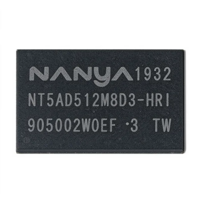
NT5AD512M16C4-HRI - 8Gb DDR4 SDRAM 512Mx16 | Nanya Technology
The Nanya Technology NT5AD512M16C4-HRI is a high-performance DDR4 SDRAM device organized as 512M x 16, providing a total density of 8 Gigabits. It operates from a 1.2V power supply and is housed in a 96-pin TFBGA package, making it suitable for space-constrained applications requiring high memory bandwidth and low power consumption. DDR4 SDRAM (Double Data Rate 4 Synchronous Dynamic Random-Access Memory) is a type of volatile memory that transfers data on both edges of the clock signal, doubling the data rate compared to DDR3. It features a prefetch buffer of 8n, allowing high-speed data access while maintaining lower operating voltages (1.2V vs 1.5V for DDR3), which reduces power consumption and heat generation. DDR4 is the industry standard for modern computing, networking, and embedded systems, offering improved reliability and performance over previous generations. Key features of the NT5AD512M16C4-HRI include an industrial temperature grade (0°C to +95°C), auto self-refresh, built-in temperature sensor, auto precharge, asynchronous reset, data mask, write leveling, dynamic on-chip termination (ODT), ZQ calibration, and CRC (Cyclic Redundancy Check) function. These features enhance signal integrity, data reliability, and system robustness, particularly in demanding industrial environments. The device supports data rates up to 3200 MT/s (per the 'H' speed grade), with a CAS latency of 22 cycles. It utilizes a 16n prefetch architecture and includes on-die ECC for improved data integrity. The 96-ball TFBGA package measures 9mm x 13mm with a 0.8mm ball pitch, offering excellent thermal and electrical performance for high-speed operation. Typical applications include industrial controllers, embedded computing modules, networking equipment, and data storage systems. The industrial temperature range and robust feature set make it ideal for applications requiring reliable operation in harsh environments, such as factory automation, transportation, and outdoor infrastructure. When designing with this DDR4 device, ensure proper termination and layout practices are followed to maintain signal integrity at high speeds. The ZQ calibration pin requires a 240-ohm resistor to ground, and the VTT and VREF supplies must be properly decoupled. Refer to the Nanya datasheet for detailed PCB layout guidelines and timing parameters.
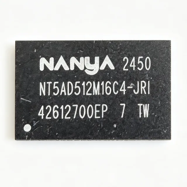
NT5AD512M16C4-JR - 8Gb DDR4-3200 SDRAM | Nanya Tech
The Nanya Technology NT5AD512M16C4-JR is a high-speed, standard DDR4 SDRAM component organized as 512M x16, providing 8Gbit of memory density. It operates from a 1.2V power supply and supports data rates up to 1.6GHz (DDR4-3200), making it suitable for a wide range of computing, networking, and industrial applications. The device is housed in a 96-ball TFBGA package, offering a compact footprint for space-constrained PCB designs. DDR4 SDRAM (Double Data Rate 4 Synchronous Dynamic Random-Access Memory) is a type of volatile memory that transfers data on both edges of the clock signal, doubling the data rate compared to its predecessor DDR3. It is a key component in modern computing systems, providing the main memory for processors, and is also used in networking equipment, industrial controllers, and embedded systems. DDR4 operates at a lower voltage (1.2V) than DDR3 (1.5V), reducing power consumption and heat generation, which is critical for high-density memory modules and portable devices. Key features of the NT5AD512M16C4-JR include auto self-refresh, a built-in temperature sensor, auto precharge, asynchronous reset, data mask, write leveling, dynamic on-chip termination (DTC), ZQ calibration, and CRC (Cyclic Redundancy Check) function. These features enhance signal integrity, reliability, and ease of integration in high-speed systems. The operating temperature range is 0°C to +95°C, making it suitable for commercial and industrial environments. Technically, the device supports a burst length of 8 and on-die termination (ODT) for improved signal quality. The ZQ calibration function allows the device to adjust its output driver and ODT impedances to match the system's characteristic impedance, reducing reflections and improving data eye margins. The CRC function provides error detection for data transmitted during write operations, enhancing data integrity in critical applications. Typical applications include consumer electronics (e.g., set-top boxes, smart TVs), industrial automation, networking systems (routers, switches), and smart IoT devices. The high density and speed make it ideal for applications requiring large memory capacity and fast data throughput, such as edge computing and real-time data processing. When designing with this component, ensure proper decoupling capacitors are placed near the power pins to minimize noise, and follow the PCB layout guidelines in the datasheet for high-speed signals to maintain signal integrity. The device requires a 1.2V VDD and a separate VPP supply (2.5V) for the wordline driver, which must be properly regulated.
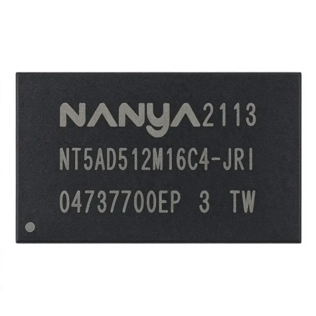
NT5AD512M16C4-JRI - 8Gb DDR4-3200 SDRAM | Nanya Technology
The Nanya Technology NT5AD512M16C4-JRI is a high-performance DDR4 SDRAM device organized as 512M x 16 bits, providing 8Gb of memory density. It operates at a clock frequency of 1.6GHz (DDR4-3200) with a supply voltage of 1.2V, and is housed in a 96-ball TFBGA package. This component is designed for a wide range of computing and embedded applications, offering high-speed data transfer and low power consumption. DDR4 SDRAM (Double Data Rate 4 Synchronous Dynamic Random-Access Memory) is a type of volatile memory that transfers data on both edges of the clock signal, effectively doubling the data rate. It is the successor to DDR3 and provides higher bandwidth, lower operating voltage (1.2V vs 1.5V), and improved signal integrity through features like on-die termination (ODT) and write leveling. DDR4 is a critical component in modern computing systems, from servers and desktops to embedded and industrial applications. Key features of the NT5AD512M16C4-JRI include auto self-refresh, built-in temperature sensor, auto precharge, asynchronous reset, data mask, write leveling, dynamic on-chip termination, ZQ calibration, and CRC (Cyclic Redundancy Check) function. These features enhance reliability and performance in demanding environments. The device supports an operating temperature range of -40°C to +95°C, making it suitable for industrial applications. The NT5AD512M16C4-JRI utilizes advanced CMOS technology and a 96-ball TFBGA package, which offers excellent thermal and electrical performance. The built-in temperature sensor enables efficient thermal management, while the ZQ calibration ensures optimal signal integrity. The CRC function provides error detection for data integrity, which is crucial for mission-critical systems. Typical applications include data storage, firmware boot, embedded logging, industrial controllers, computing modules, and replacement sourcing. Its high density and speed make it ideal for networking equipment, servers, and high-performance embedded systems. The wide temperature range and robust feature set ensure reliable operation in harsh environments. When designing with this component, ensure proper decoupling capacitors are placed near the power pins to minimize noise. The ZQ pin requires a 240-ohm resistor to ground for calibration. Follow the DDR4 layout guidelines for signal integrity, including matched trace lengths and proper termination.
NT5CB256M16CP-DI - 4Gb DDR3L SDRAM 256Mx16 | Nanya
The Nanya NT5CB256M16CP-DI is a 4Gb DDR3L SDRAM organized as 256Mx16, operating at 1.35V (DDR3L) with a 96-ball TFBGA package. It supports data rates up to DDR3-1600 (800 MHz clock) and is designed for commercial, industrial, and automotive temperature ranges. This memory device features 8 internal banks, differential clock inputs, and programmable CAS latency (CL), write latency (CWL), and additive latency. It is compliant with JEDEC DDR3L standards and offers on-die termination (ODT) for signal integrity. DDR3L SDRAM is a type of dynamic random-access memory that operates at a lower voltage (1.35V) compared to standard DDR3 (1.5V), reducing power consumption by about 20% while maintaining similar performance. It is part of the DDR3 memory family, which uses double data rate architecture to transfer data on both edges of the clock. DDR3L is widely used in mobile, embedded, and industrial applications where power efficiency is critical. Key features include a 256Mx16 organization (4Gb density), 1.35V supply voltage, 96-ball TFBGA package, and support for data rates up to 1600 Mbps/pin. The device has a programmable CAS latency of 5-11, write latency of 5-9, and additive latency of 0-13. It also features 8 internal banks, differential clock inputs, and on-die termination. The operating temperature range is -40°C to +95°C (industrial) and -40°C to +105°C (automotive). The NT5CB256M16CP-DI uses a 70nm process technology, enabling high density and low power consumption. It incorporates DLL (delay-locked loop) for precise timing, and supports self-refresh and partial array self-refresh for power saving. The device is RoHS compliant and lead-free. Typical applications include embedded systems, networking equipment, industrial automation, automotive infotainment, and solid-state drives. Its low voltage and wide temperature range make it suitable for harsh environments. When designing with this memory, ensure proper decoupling capacitors near the power pins and follow the layout guidelines in the datasheet to minimize signal integrity issues. The device requires a stable 1.35V supply and reference voltage (VREF) for optimal operation.
NT5CB256M16CP-DIH - 4Gb DDR3L SDRAM 256Mx16 | Nanya
The Nanya NT5CB256M16CP-DIH is a 4Gb DDR3L SDRAM organized as 256M x 16, operating at 1.35V (VDD/VDDQ) with a data rate of 1600Mbps (DDR3L-1600). It is housed in a 96-ball TFBGA package and supports commercial, industrial, and automotive temperature grades. This memory device is designed for high-bandwidth, low-power applications, offering a 16-bit data bus and 8 internal memory banks (BA0-BA2). DDR3L SDRAM is a type of dynamic random-access memory that operates at a lower voltage (1.35V) compared to standard DDR3 (1.5V), reducing power consumption by up to 20% while maintaining similar performance. It is part of the DDR3 memory family, which uses double data rate architecture to transfer data on both edges of the clock, and is widely used in computing, networking, and embedded systems. Key features include differential clock inputs (CK, CK#), programmable CAS Latency (CL) and WRITE Latency (CWL) of 5,6,7,8, and 9, and POSTED CAS additive latency. The device supports on-die termination (ODT) and dynamic ODT for improved signal integrity. It also features auto-refresh and self-refresh modes for low-power standby. The NT5CB256M16CP-DIH uses a 70nm process technology, enabling high density and low power. The 96-ball TFBGA package provides excellent thermal and electrical performance, with a ball pitch of 0.8mm. The device is RoHS compliant and supports industrial temperature range (-40°C to +95°C) for the -DIH variant. Typical applications include embedded computing, networking equipment, industrial automation, and automotive infotainment systems. Its low voltage and high speed make it ideal for power-sensitive designs. When designing with this memory, ensure proper decoupling capacitors near the VDD and VDDQ pins, and follow the PCB layout guidelines in the datasheet to minimize signal integrity issues. The device requires a 1.35V supply and SSTL_15 interface.
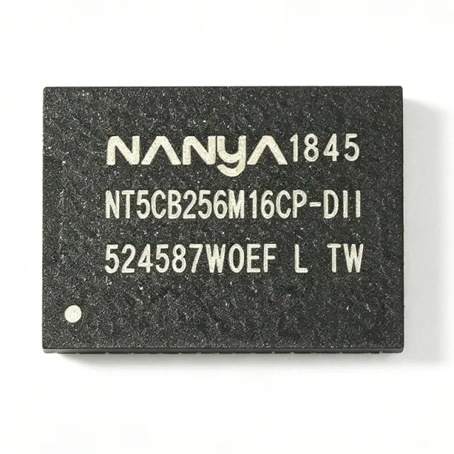
NT5CB256M16CP-DII - 4Gb DDR3L SDRAM 256Mx16 | Nanya
The Nanya NT5CB256M16CP-DII is a 4Gb DDR3L SDRAM organized as 256M x 16, operating at 1.35V with a data rate of DDR3L-1600 (CL11). It is part of Nanya's C-die family, designed for commercial, industrial, and automotive temperature grades. The device is housed in a 96-ball FBGA package, offering a compact footprint for space-constrained applications. DDR3L SDRAM (Double Data Rate 3 Low Voltage) is a type of synchronous dynamic random-access memory that operates at a lower voltage (1.35V) compared to standard DDR3 (1.5V), reducing power consumption by up to 20% while maintaining similar performance. It is widely used in computing, networking, and embedded systems where energy efficiency is critical. DDR3L is part of the DDR SDRAM family, which includes DDR, DDR2, DDR3, and DDR4, each offering increased bandwidth and lower power. Key features include a 16-bit data bus, 8 internal banks, burst lengths of 8 and 4 (with burst chop), on-die termination (ODT), and programmable CAS latency. The device supports auto-refresh and self-refresh modes, with a refresh interval of 7.8us at 85C and 3.9us at 95C. It also features a temperature-compensated self-refresh (TCSR) for improved reliability in high-temperature environments. The NT5CB256M16CP-DII utilizes Nanya's advanced C-die process technology, enabling high density and low power. The memory operates from a 1.35V core supply and a 1.5V I/O supply (for DDR3L, VDDQ is 1.35V). It supports data transfer rates up to 1600 Mbps per pin, providing a peak bandwidth of 3.2 GB/s per device. The device includes a programmable mode register for configuring CAS latency, burst length, and other operating parameters. Typical applications include embedded computing, networking equipment (routers, switches), industrial automation, and automotive infotainment systems. Its low voltage and high density make it ideal for power-sensitive designs, while the industrial temperature range (-40C to +95C) ensures reliable operation in harsh environments. When designing with this device, ensure proper decoupling capacitors near the power pins and follow the PCB layout guidelines in the datasheet to minimize signal integrity issues. The device requires a stable 1.35V supply and a separate VDDQ supply; both must be within specified tolerances.
NT5CB256M16CP-EK - 4Gb DDR3L SDRAM 256Mx16 | Nanya
The Nanya NT5CB256M16CP-EK is a 4Gb DDR3L SDRAM organized as 256M x 16, operating at 1.35V (DDR3L) with a 96-ball TFBGA package. It supports data rates up to DDR3-2133 (CL14) and is designed for commercial, industrial, and automotive temperature grades. The device features 8 internal memory banks, differential clock inputs (CK, CK#), and programmable CAS Latency (CL), WRITE Latency (CWL), and Posted CAS Additive Latency. With a 16-bit data bus, it is ideal for applications requiring high-density, low-power memory in compact form factors. DDR3L SDRAM (Double Data Rate 3 Low Voltage) is a type of synchronous dynamic random-access memory that operates at 1.35V, reducing power consumption by about 20% compared to standard 1.5V DDR3. It is part of the DDR3 family, which uses double data rate signaling to transfer data on both edges of the clock, achieving high bandwidth. DDR3L is commonly used in mobile, embedded, and industrial systems where power efficiency is critical, and it is backward compatible with DDR3 through its support for both 1.35V and 1.5V operation. Key features include a 4Gb density, 256M x 16 organization, 96-ball TFBGA package, and support for data rates up to 2133 Mbps. The device operates from a 1.35V supply (1.425V to 1.575V range) and features programmable CAS Latency (CL) of 9, 10, 11, 12, 13, and 14, and WRITE Latency (CWL) of 5, 6, 7, 8, and 9. It also supports on-die termination (ODT), dynamic ODT, and programmable output driver impedance. The industrial and automotive temperature grades ensure reliable operation from -40°C to +95°C (case temperature). Technically, the NT5CB256M16CP uses a 30nm-class DRAM process, enabling high density with low power. The device includes 8 internal banks (BA0-BA2) for efficient interleaving and reduced row activation overhead. Differential clock inputs (CK, CK#) improve signal integrity, and the programmable additive latency (AL) supports posted CAS operations for improved bus efficiency. The device also features auto refresh and self refresh modes, with a typical refresh period of 7.8us at 85°C and 3.9us at 95°C. Typical applications include embedded computing, networking equipment, industrial automation, automotive infotainment and ADAS, and high-performance consumer electronics. The 256M x 16 organization is well-suited for systems requiring a 16-bit memory bus, such as SoCs and FPGAs with wide memory interfaces. The low-voltage operation makes it ideal for battery-powered and thermally constrained designs. When designing with this device, ensure proper decoupling with 0.1uF and 1uF capacitors near the power pins, and follow the PCB layout guidelines for DDR3 routing, including matched trace lengths and impedance control (typically 40-50 ohms). The VREFCA and VREFDQ should be decoupled with 0.1uF capacitors to ground.
NT5CC256M16CN-FLB - 4Gb DDR3L SDRAM | Nanya Technology
The Nanya Technology NT5CC256M16CN-FLB is a 4Gb (256M x 16) DDR3L SDRAM designed for commercial, industrial, and automotive applications. It operates at a supply voltage of 1.35V (DDR3L) and supports data rates up to 1866 Mbps (PC3-14900). The device is housed in a 96-ball FBGA package, offering a compact footprint for space-constrained designs. DDR3L SDRAM is a type of double data rate synchronous dynamic random-access memory that operates at a lower voltage (1.35V) compared to standard DDR3 (1.5V), reducing power consumption by up to 20% while maintaining high bandwidth. It is part of the DDR3 memory family, which uses an 8n prefetch architecture and on-die termination (ODT) to improve signal integrity at high speeds. DDR3L is widely used in mobile devices, embedded systems, and industrial computing where power efficiency is critical. Key features include a 16-bit I/O interface, 8 internal banks, burst lengths of 8 and 4 (with burst chop), programmable CAS latency (CL) of 9, 10, 11, and 13, and a self-refresh mode for low-power standby. The device supports auto precharge, write leveling, and ZQ calibration for improved signal integrity. It also includes a temperature sensor for thermal management, enabling dynamic refresh rate adjustment. The NT5CC256M16CN-FLB uses a 30nm-class process technology, achieving high density with low power consumption. The FBGA package provides excellent thermal and electrical performance, with a thermal resistance of [DATA_NEEDED: theta_JA]. The device is RoHS compliant and supports industrial temperature ranges from -40°C to +95°C (case temperature). Typical applications include solid-state drives (SSDs), network routers, industrial PCs, automotive infotainment systems, and embedded computing platforms. Its low voltage and high speed make it ideal for power-sensitive designs that require high memory bandwidth. When designing with this device, ensure proper decoupling capacitors near the VDD and VDDQ pins, and follow the PCB layout guidelines in the datasheet to minimize signal reflections. The device requires a stable 1.35V supply and a reference voltage (VREF) for the address/command bus.
NT5CC256M16CN-FLH - 4Gb DDR3L SDRAM | Nanya Technology
The Nanya Technology NT5CC256M16CN-FLH is a 4Gb (256M x 16) DDR3L SDRAM designed for commercial, industrial, and automotive applications. It operates at a supply voltage of 1.35V (DDR3L) with a data rate of up to 1866 Mbps (PC3-14900). The device is housed in a 96-ball FBGA package, offering a compact footprint for space-constrained designs. DDR3L SDRAM is a type of dynamic random access memory that operates at a lower voltage (1.35V) compared to standard DDR3 (1.5V), reducing power consumption by approximately 20% while maintaining high bandwidth. It is part of the DDR3 memory family, which uses an 8n-prefetch architecture to achieve high data rates. DDR3L is widely used in computing, networking, and embedded systems where power efficiency is critical. Key features include a 16-bit I/O interface, 8 internal banks, burst lengths of 8 and 4 (with burst chop), on-die termination (ODT), and programmable CAS latency. The device supports auto self-refresh, auto precharge, and write leveling for signal integrity. It also includes a ZQ calibration function for improved timing accuracy. The NT5CC256M16CN-FLH is built on Nanya's advanced DRAM process technology, ensuring high reliability and performance. It supports a temperature range of 0°C to +95°C (TC) for commercial and industrial grades, with automotive grade options available. The device is RoHS compliant and lead-free. Typical applications include DDR3L memory modules for laptops, servers, networking equipment, industrial PCs, and automotive infotainment systems. Its low voltage and high density make it ideal for power-sensitive designs. When designing with this device, ensure proper decoupling capacitors near the power pins and follow the layout guidelines in the datasheet to minimize signal integrity issues. The device requires a 1.35V supply and a separate VDDQ for the I/O, which should be regulated accurately.
NT5CC256M16CN-FLI - 4Gb DDR3L SDRAM | Nanya Technology
The Nanya Technology NT5CC256M16CN-FLI is a 4Gb (256M x 16) DDR3L SDRAM designed for commercial, industrial, and automotive applications. It operates at a supply voltage of 1.35V (DDR3L) with a data rate of up to 1866 Mbps (PC3-14900). The device is available in a 96-ball TFBGA package, offering a compact footprint for space-constrained designs. DDR3L SDRAM is a type of dynamic random-access memory that operates at a lower voltage (1.35V) compared to standard DDR3 (1.5V), reducing power consumption by approximately 20% while maintaining similar performance. It is part of the DDR3 memory family, which uses double data rate architecture to transfer data on both edges of the clock signal, and is widely used in computing, networking, and embedded systems. Key features include a 16-bit I/O interface, 8 internal banks, burst lengths of 8 and 4 (with burst chop), on-die termination (ODT), and programmable CAS latency. The device supports auto self-refresh and auto precharge functions, ensuring data integrity with minimal power. It also includes write leveling, data mask, and ZQ calibration functions for signal integrity and system reliability. The NT5CC256M16CN-FLI is fabricated using Nanya's advanced DRAM process technology, providing high density and low power consumption. It supports a temperature range of 0°C to +95°C (case temperature) for industrial applications, with derating required above 95°C. The device is RoHS compliant and lead-free, meeting environmental standards. Typical applications include DDR3L memory modules for laptops, embedded systems, networking equipment, and industrial computing. Its low voltage and high speed make it ideal for power-sensitive designs, while the industrial temperature range supports harsh environments. When designing with this device, ensure proper decoupling capacitors near the power pins and follow the PCB layout guidelines in the datasheet to minimize signal integrity issues. The device requires a stable 1.35V supply and a 0.75V reference voltage for the address/command bus.
NT5CC256M16CN-FLNA - 4Gb DDR3L SDRAM 256Mx16 | Nanya
The Nanya Technology NT5CC256M16CN-FLNA is a 4Gb DDR3L SDRAM organized as 256M words by 16 bits, designed for commercial, industrial, and automotive applications. It operates at a supply voltage of 1.35V (DDR3L) with a 1.5V tolerant option, supporting data rates up to 1866 Mbps. The device is housed in a 96-ball FBGA package, offering a compact footprint for high-density memory systems. DDR3L (Low Voltage DDR3) is a type of synchronous dynamic random-access memory that operates at a lower voltage (1.35V) compared to standard DDR3 (1.5V), reducing power consumption by up to 20% while maintaining similar performance. It is part of the DDR3 SDRAM family, which uses double data rate architecture to transfer data on both edges of the clock, and is widely used in computing, networking, and embedded systems. Key features include a 16n prefetch architecture, on-die termination (ODT), programmable CAS latency, and burst lengths of 8 and 4. The device supports auto-refresh and self-refresh modes, with a temperature-compensated self-refresh (TCSR) for industrial temperature ranges. It also features a programmable output driver impedance and a DLL for precise timing. Technically, the NT5CC256M16CN-FLNA uses a 30nm-class process technology, achieving high density with low power. The memory array is organized into 8 banks, each with 32K rows, providing efficient row activation and precharge. The device includes a mode register set (MRS) for configuration, and supports write leveling and read leveling for improved signal integrity in high-speed systems. Typical applications include DDR3L memory modules for laptops, servers, and industrial PCs, as well as embedded systems such as network routers, set-top boxes, and automotive infotainment. Its low voltage and wide temperature range make it suitable for battery-powered and harsh environments. When designing with this device, ensure proper decoupling capacitors near the VDD and VDDQ pins, and follow the PCB layout guidelines for DDR3L to maintain signal integrity. The device requires a stable 1.35V supply and a reference voltage (VREF) for the address and control signals.