Управление питанием
Подкатегории
Товары (2819)

ITS428L2ATMA1 - 5.8A Smart High-Side Power Switch | Infineon
The Infineon ITS428L2ATMA1 is a 5.8A single-channel smart high-side power switch in a PG-TO252-5-11 (TO-252-5 / DPAK-4 leads + tab) surface-mount package. It monolithically integrates a vertical N-channel power MOSFET with a charge pump, ground-referenced CMOS-compatible input, and diagnostic feedback, and is fabricated using Infineon's Smart SIPMOS technology. The part targets 5 V, 12 V, and 24 V DC grounded industrial loads and is part of the PROFET Industrial family. A high-side switch is a power-distribution topology in which the load is tied to ground and the switch sits between the positive supply rail and the load. Compared with low-side switching, high-side architecture eliminates a permanent ground path, simplifies fault detection, and protects downstream wiring from shorts to ground. Smart high-side switches add on-chip protection (overload, short-circuit, overvoltage/load-dump, overtemperature) and a status/diagnostic output that the microcontroller can read for fault handling. Key features of the ITS428L2ATMA1 include a typical on-resistance in the low milli-ohm range for low conduction loss, a continuous load current capability up to approximately 5.8 A, CMOS-compatible logic input for direct 3.3 V or 5 V micro-controller drive, integrated overvoltage protection including load dump via an external resistor, and a diagnostic feedback pin for open-load, short-to-ground, short-to-battery, and overtemperature reporting. The PROFET family is engineered to handle high inrush currents typical of lamps, solenoids, motors, and capacitive loads. Typical applications include industrial 24 V PLC digital outputs, relay and solenoid replacement, automotive body and chassis modules (12 V), building automation, and any general resistive, inductive, or capacitive 5 V - 24 V load. When designing with this part, ensure the supply voltage stays within the supported range, add the recommended external resistor for overvoltage/load-dump clamping, and observe thermal limits at maximum continuous current. The TO-252-5 package requires sufficient copper pad area for heat dissipation. This page aggregates distributor pricing, drop-in PROFET family alternatives, and practical design notes beyond the manufacturer datasheet.

ITS42K5DLDFXUMA1 - Dual 250mA PROFET High-Side Switch | Infineon
The Infineon ITS42K5DLDFXUMA1 is a dual-channel high-side power switch from the PROFET (Protected MOSFET) 24V/48V family, delivering two independent 250 mA channels in a compact 10-pin PG-TSON-10-2 (TSON EP) exposed-pad package. Each channel integrates a P-channel power MOSFET with on-state resistance of 2.5 ohm and a built-in freewheeling diode, providing clamped inductive-load switching up to 13.5 V supply operation. A PROFET high-side switch is a smart power switch that combines a MOSFET output stage, gate driver, and comprehensive protection circuitry in one IC. It belongs to the power distribution switch category within the broader power management IC (PMIC) hierarchy, sitting between discrete MOSFETs (which need external drivers and protection) and fully-integrated system basis chips (which add CAN/LIN transceivers). PROFET switches are commonly used in automotive body and powertrain modules where they replace discrete relays with PCB-mountable, diagnostically-rich equivalents. Key features include dual 250 mA continuous current per channel, 2.5 ohm Rds(on) typical, integrated freewheeling diode per output, status feedback, and protection functions (overload, short-circuit, thermal shutdown, overvoltage clamp). The 1:1 input-to-output switch topology provides simple logic-level control from a microcontroller GPIO. Operating voltage range supports both 12 V and 24 V automotive buses with reverse-battery robustness. Architecturally, each channel uses a vertical P-channel DMOS output transistor driven by a charge-pump-derived gate drive, with current-sensing and temperature-sensing blocks feeding back into a fault-management state machine. The exposed thermal pad on the bottom of the TSON-10-2 package provides a low thermal-resistance path (~30 C/W typical) to the PCB copper, enabling sustained operation at the rated current without external heatsinking. Typical applications include automotive body control modules (BCM), HVAC actuators, LED lighting drivers, sensor power distribution, and industrial 24V PLC outputs. The dual-channel design is particularly efficient for paired loads such as bidirectional motors or two indicator lamps sharing one IC. When designing with this part, place the exposed pad on a copper pour of at least 1 square centimeter to keep junction temperature within rating at full load. The status pin requires a pull-up resistor; consult the datasheet for diagnostic truth-table behavior in fault conditions. This page synthesizes Infineon datasheet parameters, distributor pricing, drop-in alternatives, and practical design notes not found on a single distributor product page, giving engineers a one-stop reference for evaluation and BOM decisions.

ITS4300SSJDXUMA1 - 400mA Smart High-Side Switch | Infineon
The Infineon ITS4300SSJDXUMA1 is a 400 mA smart high-side power switch with an integrated vertical N-channel power FET, housed in a PG-DSO-8 package. It provides embedded protection and diagnostic functions for 12 V and 24 V DC industrial applications, with a low typical on-state resistance of 300 mΩ and CMOS-compatible control interface. A high-side power switch (also called a smart high-side driver or PROFET) is a type of power distribution switch that sits between the supply rail and the load, replacing discrete MOSFETs, fuses, and relay circuits. The category hierarchy is: high-side switch -> load driver -> power distribution switch -> PMIC (Power Management IC) -> semiconductor. Smart high-side switches integrate overcurrent, short-circuit, thermal, overvoltage, and undervoltage protection, dramatically simplifying the BOM and improving system reliability. Key features include overload protection with current limitation, short-circuit protection, thermal shutdown with auto-restart, overvoltage protection including load-dump, shutdown on undervoltage, fast demagnetization of inductive loads, and ESD protection. The CMOS-compatible input makes it directly compatible with 3.3 V and 5 V microcontrollers. The device is qualified for industrial applications per JEDEC JESD47. Technically, the ITS4300S uses a vertical N-channel DMOS output stage driven by a charge pump that generates the gate boost voltage needed for full enhancement of the high-side FET. The integrated charge pump, current sense, and protection logic are all on a single piece of silicon, achieving a typical RDS(on) of 300 mΩ at 25°C. The fast demagnetization circuit handles the inductive kickback of relays, solenoids, and small motors, allowing unclamped inductive switching up to the device's internal energy rating. Typical applications include driving resistive, inductive, and capacitive loads in industrial automation, programmable logic controllers (PLCs), sensor power distribution, electromagnetic relay drivers, and any 12 V/24 V high-side switching application with low standby current requirements. The part is also used as a power management switch for low-current standby rails. When designing with this device, ensure the load current stays below 400 mA continuous and that the inductive load's energy does not exceed the device's single-pulse avalanche rating. A reverse-polarity protection diode or P-channel FET is recommended at the supply input since the ITS4300S does not include internal reverse-battery protection. Good PCB layout practices (wide traces, short ground returns) help minimize voltage transients. This page synthesizes distributor pricing, drop-in PROFET alternatives, and practical design notes not found in the manufacturer datasheet alone.
ITS4880R - 8-Ch 0.625A Smart High-Side Switch | Infineon
The Infineon ITS4880R is an 8-channel smart high-side power switch (PROFET Industrial family) delivering 0.625 A per channel for 24 V DC industrial loads, monolithically integrated in Smart SIPMOS technology. Each of the eight channels features an N-channel vertical power FET with charge pump, ground-referenced CMOS or Vbb/2-compatible input, and common diagnostic feedback, housed in a PG-DSO-36-26 power package. Operating supply range spans roughly 11 V to 45 V with 60 V load-dump transient capability for direct 24 V industrial bus use. A high-side switch is a power-distribution topology that places the MOSFET between the supply rail and the load, allowing logic-level signals to switch the grounded load safely. Within the broader semiconductor hierarchy, the ITS4880R sits in the PMIC > Power Distribution Switch / Load Driver category, often called a smart power switch or PROFET (Protected FET) when diagnostic and protection features are integrated. The 8-channel parallel architecture lets one IC replace eight discrete low-side drivers plus protection circuitry, reducing PCB area and BOM count in 24 V multi-load systems. Key features include 0.625 A nominal per-channel current, 8 independently controlled inputs, integrated charge pump for full N-channel enhancement, common diagnostic output, embedded protection (overload, short-circuit, over-temperature, ESD, and over-voltage clamp), and CMOS or Vbb/2 input compatibility. The common-diagnostic feedback pin reports open-load and overtemperature conditions to the host MCU, simplifying firmware state machines. Internally the ITS4880R combines a vertical DMOS output stage with a charge-pump gate driver and per-channel protection logic on a single Smart SIPMOS die. The Vbb/2 input option allows direct connection to 5 V microcontrollers without level shifters. Common diagnostic feedback consolidates eight per-channel fault signals into one pin, saving MCU GPIOs and reducing wiring complexity in 24 V PLC and industrial-automation backplanes. Typical applications include 24 V industrial automation (PLC digital outputs), process-control solenoid and valve drivers, building-automation relay replacement, sensor and indicator power distribution, machine-tool lamp and actuator control, and HVAC damper/valve arrays. The wide Vbb tolerance and load-dump rating make it well suited to factory-floor environments with long cable runs and inductive transients. When designing with this device, derate per-channel current to roughly 0.4-0.5 A continuous when all eight channels conduct simultaneously, because the PG-DSO-36-26 package shares thermal capacity. Always place a reverse-polarity and TVS clamp on Vbb, and use series inductance mitigation (freewheel diode or TVS) when switching solenoids or relays. This page synthesizes distributor pricing, drop-in alternatives from the Infineon PROFET family, and practical PCB design notes for 24 V industrial loads not found in the manufacturer datasheet alone.
ITS6080SEPDXUMA1 - 8A Smart High-Side Switch | Infineon
The Infineon ITS6080SEPDXUMA1 is a single-channel smart high-side power switch from Infineon's PROFET Industrial 75 mOhm family, delivering up to 8A continuous output current in a 14-pin PG-TSDSO package with exposed thermal pad. The device integrates a vertical N-channel power MOSFET with 75 mOhm typical on-state resistance, comprehensive protection features, and diagnostic feedback, designed for 12V and 24V industrial and automotive load-driving applications. A high-side switch (HSS) is a power distribution IC that sits between a positive supply rail and a load, allowing a low-voltage logic signal (typically 3.3V or 5V microcontroller GPIO) to control a much larger load current while providing protection against overloads, short circuits, and thermal faults. Compared with a discrete MOSFET plus fuse solution, an intelligent high-side switch integrates the power transistor, charge pump gate drive, current sense, and fault diagnostics into a single package, reducing PCB area, BOM count, and design complexity. The ITS6080 belongs to the family tree: high-side switch -> power distribution switch -> power management IC -> semiconductor. Key specifications include 75 mOhm typical on-resistance at 25C, an operating supply range of 5V to 34V (with load-dump survival up to 62V), 8A continuous drain current, and integrated protections including overload current limiting, short-circuit shutdown, thermal shutdown, over-voltage clamp, and ESD protection. The device offers proportional load current sense output for diagnostic monitoring and an active-low fault feedback pin for system-level safety. The ITS6080 employs a vertical DMOS output stage with an integrated charge pump that fully enhances the N-channel MOSFET regardless of supply voltage, achieving true low-Rds(on) across the full operating range. This contrasts with older P-channel high-side architectures that suffer from higher on-resistance at low supply voltages. The device is qualified to AEC-Q100 for automotive harsh environments. Typical applications include driving resistive, inductive, and capacitive loads such as solenoids, valves, relay coils, LED strings, motors, and heaters in body electronics modules, industrial automation PLCs, and process control systems. The 8A rating suits medium-power actuators where a robust, self-protected switch replaces discrete solutions. When designing with this device, derate the load current for ambient temperature and PCB copper area. Use a 100nF ceramic decoupling capacitor directly at Vbb and follow the application note's PCB layout guidelines to ensure the exposed pad dissipates heat efficiently into the copper plane. This page consolidates distributor pricing, PROFET family variants, and PCB layout recommendations not present in the standalone datasheet, providing a single engineering reference.
ITS711L1FUMA1 - 4-Ch Smart High-Side Switch 1.7A PG-DSO-20 | Infineon
The Infineon ITS711L1FUMA1 is a 4-channel smart high-side power switch built on Smart SIPMOS technology, housed in a PG-DSO-20-31 package and rated for 1.7A continuous output current per channel (4A total package capability). It operates over a load voltage range of 5V to 34V, making it directly suited to industrial 12V and 24V DC grounded load systems. Key features include an integrated charge pump for N-channel vertical power FET operation, ground-referenced CMOS-compatible logic inputs, embedded diagnostic feedback for each channel, and monolithic protection functions including over-load, over-voltage, over-temperature, and short-circuit handling. The PROFET (Protected FET) Industrial family design replaces electromechanical relays and discrete MOSFET driver circuits, providing a single-chip solid-state solution. The ITS711L1 is a member of the high-side switch category within the broader power distribution switch hierarchy. High-side switches sit between the supply rail and the load (versus low-side switches which sit between load and ground), allowing them to provide complete load disconnect and ground-referenced control logic. The 1:1 input-to-output ratio and four parallel outputs make this part suitable for driving multiple resistive, inductive, or capacitive loads from a single microcontroller I/O bus. Technical depth: the device integrates four vertical N-channel power MOSFETs, a charge pump to drive the high-side gates above the supply rail, CMOS input buffers, and per-channel sense/current-limit circuitry. Diagnostic feedback (open-drain status) lets the host microcontroller distinguish normal operation from open-load, short-to-ground, short-to-battery, and thermal shutdown events. The Smart SIPMOS process combines a vertical DMOS power stage with CMOS control logic on a single die. Typical applications include industrial automation PLC outputs, 24V solenoid and valve drivers, building management relay replacement, programmable logic controller (PLC) discrete outputs, and machine safety interfaces. The wide 5V-34V input range covers both 12V automotive subsystems and 24V industrial battery-backed rails. When designing with the ITS711L1FUMA1, derate output current at elevated ambient temperatures following the thermal resistance curve in the datasheet, and place sufficient copper pour under the exposed pad to keep junction temperature below the shutdown threshold. Inputs are CMOS-compatible, eliminating the need for level-shifters in 3.3V or 5V microcontroller systems. This page synthesizes distributor pricing, drop-in alternatives, and practical design notes not found in the manufacturer datasheet, helping engineers select and qualify the ITS711L1FUMA1 for production designs.
ITS716GFUMA1 - 4-Ch Smart High-Side Switch 2.3A | Infineon
The Infineon ITS716GFUMA1 is a 4-channel smart high-side power switch with integrated vertical power MOSFETs, delivering 2.3 A continuous current per channel in a PG-DSO-20-32 (20-pin SOIC) package. It provides embedded protection (overload, short-circuit, over-temperature, over-voltage) and diagnostic feedback for microcontroller-driven 12 V and 24 V DC grounded loads in industrial applications. A smart high-side switch is a semiconductor relay that sits between the supply rail and the load, replacing electromechanical relays and fuses. Unlike a simple MOSFET, it integrates logic-level GPIO control, current sensing, slew-rate limiting, and fault reporting into a single IC. The ITS716GFUMA1 belongs to Infineon's PROFET Industrial family, which targets PLC I/O, process automation, and building-control systems where the device must survive harsh electrical environments and inductive load transients. Key features include four independent channels each rated up to 2.3 A, SPI-compatible diagnostic feedback (open-load, short-to-ground, short-to-battery, overtemperature), very low standby current, and broad operating voltage from 5 V to 36 V (load-dump tolerant to 45 V). The vertical power FET topology minimizes on-resistance per channel while maintaining a small footprint. The PG-DSO-20-32 exposed-pad package provides a low thermal resistance of about 36 C/W, enabling sustained operation across multiple parallel channels in industrial cabinets. The device is engineered for direct connection to a microcontroller's GPIO pins through its parallel input interface, with one logic input per channel plus a shared enable and diagnostic output. The internal charge pump and gate driver handle PWM operation up to 1 kHz for LED dimming or solenoid proportional control without external driver components. The ITS716GFUMA1 is qualified to Infineon's industrial grade (-40 C to +85 C ambient) with extended ESD and transient immunity per IEC 61000-4. Typical applications include industrial PLC digital outputs, 24 V solenoid and valve drivers, LED indication and lighting strips, relay replacement in HVAC and building automation, and ground-switched load management in process control panels. Each channel independently drives resistive, inductive, or capacitive loads including incandescent lamps with inrush currents well above the steady-state rating. When designing with the ITS716GFUMA1, ensure a 100 nF ceramic bypass capacitor on Vbb close to the IC and adequate PCB copper under the exposed pad for thermal dissipation. The diagnostic feedback pin requires a pull-up resistor to the microcontroller supply; software must debounce fault events because inrush loads (e.g., incandescent lamps) momentarily exceed the current-limit threshold and trip fault flags. This page synthesizes distributor pricing, drop-in same-brand alternatives, and practical design notes not found in the manufacturer datasheet, structured for both human review and AI-search citation.
ITS724GFUMA1 - 4-Ch 3A Smart High-Side Switch | Infineon
The Infineon ITS724GFUMA1 is a 4-channel high-side vertical power MOSFET switch rated at 3.3 A continuous per channel, integrating charge pump, CMOS-compatible ground-referenced inputs, diagnostic feedback and overvoltage protection in Infineon's Smart SIPMOS technology, housed in a 20-pin PG-DSO-20-32 surface-mount package. Designed for 12 V and 24 V industrial DC loads, the device operates across a -10 V to 16 V supply range and provides embedded protective functions including current limiting, overtemperature shutdown, and load-dump protection with external resistor. The monolithic integration eliminates the need for discrete fuses, relays and protection circuitry. A smart high-side switch is a semiconductor relay used in industrial automation and automotive electronics to switch DC loads (solenoids, lamps, motors, valves) on the positive supply rail while providing diagnostic feedback to the microcontroller. The high-side topology allows the load to be grounded, simplifying wiring harness design and improving short-to-ground detection. As a member of Infineon's PROFET (Protected MOSFET) family, the ITS724G is part of the broader category of protected switches that sit between the system power management IC and the final power distribution stage. Key features of the ITS724GFUMA1 include four independently controlled 3.3 A channels with 65 mΩ typical on-resistance per channel, open-drain status flag output for fault reporting, and an integrated charge pump that drives the gate of the N-channel power MOSFET. The device supports PWM operation for dimming or speed control and tolerates high inrush currents typical of incandescent lamp and motor loads. Reverse battery protection is provided by the inherent body diode configuration, and the device is qualified to JEDEC standards for industrial temperature ranges. Typical applications include 24 V industrial PLC output modules, automotive body electronics (door locks, window lifters, seat controllers), process control valve drivers, and LED driver modules. The wide operating voltage window and built-in diagnostics make it well suited for IEC 61131-2 compliant industrial control equipment and Profibus/CAN-connected distributed I/O. When designing with the ITS724G, derate output current according to the JEDEC EIA/JESD51 4-layer board thermal model - the PG-DSO-20-32 package has a junction-to-ambient thermal resistance in the 65-85 C/W range that limits continuous current at elevated ambient temperatures. Always connect the diagnostic status pin to a pull-up resistor and decouple the Vbb supply with at least 100 nF placed within 5 mm of the IC pins.

IW3616 - 12W Dimmable LED Driver IC | Renesas/Dialog
The Renesas (formerly Dialog Semiconductor / iWatt) IW3616 is a two-stage AC/DC digital power controller designed for high-power-factor dimmable LED drivers up to 12W. It combines power factor correction (>0.95), low total harmonic distortion (<15%), and low output ripple (<20%) in a SOIC-14 package, targeting residential and commercial dimmable retrofit LED luminaires. The IW3616-00 and IW3616-01 variants share the same silicon and footprint, with minor firmware mapping differences for dimmer compatibility. An AC/DC LED driver controller is a power management IC that converts mains AC voltage into a regulated DC current suitable for driving high-brightness LEDs. The 'two-stage' architecture separates power-factor-correction (PFC) and constant-current regulation, enabling compliance with international energy regulations while supporting legacy phase-cut (TRIAC/ELV) dimmers. Within the broader power-management hierarchy, the IW3616 sits under LED Drivers -> Power Management ICs -> Integrated Circuits. Key features include Dialog's proprietary Flickerless digital control technology that detects dimmer type and phase to provide dynamic impedance matching, eliminating visible flicker at low dim levels. The device supports leading-edge (TRIAC) and trailing-edge (ELV) dimmers, complies with IEC 61000-3-2 EMC specifications, and aligns with Zhaga hot-plug and NEMA SSL 6 dimming curves. Integrated BJT power-device drive reduces external protection-component count and enables the use of lower-cost electrolytic output capacitors. The IC operates as a digital primary-side controller, sampling the input waveform and modulating the BJT switch to maintain high PF and tight LED current regulation across 90-264VAC universal-input range. Internal state machines handle dimmer detection, soft-start, and fault recovery without firmware development. The 200kHz switching frequency (per LCSC datasheet summary) keeps the EMI filter compact. Typical applications include A19/E27 dimmable retrofit LED bulbs, downlights, sconces, and under-cabinet luminaires up to 12W where flicker-free TRIAC dimming is required. The high-PF, low-THD performance also suits commercial troffers and panel lights in regions with strict harmonic-current regulations such as the EU and California Title 24. Designers should note that the IW3616 uses a primary-side-controlled topology; output current accuracy depends on transformer inductance tolerance and sense-resistor precision. Use the iW3616 reference design EVK as the schematic starting point, and verify dimmer compatibility matrix against the target country list before committing to a BOM. This page synthesizes distributor pricing from LCSC and Mouser, drop-in family variants, and practical dimmer-compatibility notes not consolidated on the OEM product page.
IW3616-01 - Flickerless 12W High-PF Off-Line LED Driver | Renesas
The Renesas (formerly Dialog Semiconductor) IW3616-01 is a two-stage, solid-state lighting (SSL) AC/DC off-line LED driver controller that combines high power factor (>0.95), low total harmonic distortion (<15%), and low output ripple (<20%) for dimmable LED retrofit luminaires up to 12 W. Housed in a 14-pin SOIC package, the device uses a BJT power switch architecture that reduces external protection components and supports lower-cost electrolytic output capacitors compared to MOSFET-based solutions. An LED driver is an AC/DC or DC/DC power converter that delivers a regulated constant current to a string of LEDs, ensuring consistent luminance and protecting the LEDs from line-voltage transients. Two-stage architectures use a power-factor-correction (PFC) front end followed by an isolated or non-isolated DC/DC stage, which separates the high-frequency energy storage from the dimming interface. The iW3616 sits within the broader power management IC hierarchy: LED driver -> AC/DC controller -> power management IC -> semiconductor. Key features of the IW3616-01 include flickerless dimming with both leading-edge (TRIAC) and trailing-edge (ELV) dimmer detection, IEC 61000-3-2 EMC compliance, Zhaga hot-plug interface compatibility, NEMA SSL 6 dimming curve mapping, and integrated protection (LED open-circuit, short-circuit, over-temperature, and over-voltage). The 200 kHz PWM switching frequency keeps the magnetic footprint small for compact lamp form factors. The iW3616-01 applies advanced digital control to detect the dimmer type and phase angle, providing dynamic impedance to interface the dimmer and control LED brightness simultaneously. By using a BJT power device instead of a MOSFET, it reduces component count in protection circuits and enables lower-cost electrolytic capacitor usage, making it attractive for cost-sensitive residential and commercial retrofit bulb designs. Typical applications include dimmable A19/E26/E27 retrofit bulbs, downlights, candelabras, and commercial troffers where flicker-free operation across a wide dimming range is mandatory. The high-PF and low-THD characteristics also make it suitable for regions enforcing strict harmonic current regulations such as the EU, California Title 24, and Energy Star requirements. When designing with the IW3616-01, use the manufacturer's reference design to select the input bulk capacitor, BJT switch, and snubber components, and follow the layout guidelines to keep the high-current loop area small for EMI compliance.

IXCP10M90S - 900V 100mA Switchable Current Regulator | IXYS
The IXYS IXCP10M90S is a 900V minimum breakdown, 1mA to 100mA switchable current regulator housed in an industry-standard JEDEC TO-220-3 package, delivering 40W of continuous power dissipation. It combines a high-voltage current source with an integrated on/off control pin (gate) that allows the current output to be switched by applying a negative voltage to the control terminal, while a resistor between the negative terminal and ground programs the regulated current setpoint. A current regulator is a two-terminal (or three-terminal when controllable) semiconductor that maintains a constant output current over a wide range of applied voltage and temperature. Unlike a series voltage regulator, a current regulator is placed in series with the load to enforce a defined current, making it ideal for high-impedance circuits, current references, and protection stages. The IXCP10M90S belongs to the linear regulator family, specifically the constant-current subset, and is closely related to current limiting diodes (CLDs) but with the added advantage of programmable current and electronic switching. Key features include 900V minimum breakdown voltage (protecting against high-voltage transients), 1mA to 100mA programmable current range via external resistor, low temperature coefficient achieved through threshold compensation, 40W continuous dissipation, and the integrated gate control pin for on/off switching. The JEDEC TO-220 outline ensures compatibility with standard heatsink hardware, while the S-class designation refers to IXYS' enhanced switchable current regulator family. Architecturally, the IXCP10M90S uses a high-voltage bipolar JFET process with on-chip threshold compensation, yielding a temperature-stable current source. The control pin functions as a JFET gate; applying a negative bias below the pinch-off threshold disables current flow, while leaving the pin open or tied high enables normal operation. This design enables fast on/off switching without breaking the high-voltage path. Typical applications include start-up circuits for switch-mode power supplies, PABX current sources and line terminations, highly stable voltage references, surge limiters and voltage protection, fast-acting non-destructive fuses, and biasing networks for high-voltage sensor arrays. Industrial 24V loop-powered instrumentation also benefits from its wide compliance range. Designers should size the heatsink for worst-case continuous dissipation, observe the 900V breakdown derating over temperature, and add a TVS across the device when used in inductive circuits to clamp turn-off transients. Bypass the gate pin with a small capacitor to improve noise immunity in electrically noisy environments. This page synthesizes IXCP10M90S distributor pricing, drop-in alternatives from the IXYS S-class family, and practical design notes not consolidated in the manufacturer datasheet alone.

IXDD609SI - 9A Low-Side Ultrafast MOSFET/IGBT Gate Driver | IXYS
The IXYS IXDD609SI is a 9A peak source/sink low-side gate driver IC in an 8-pin SOIC with an exposed pad (8-SOIC-EP), configured as a non-inverting driver with an enable input. It operates from a wide 4.5V to 35V supply, supports logic inputs that withstand negative swings down to -5V, and produces rise/fall times below 25ns, making it one of the fastest high-current gate drivers in its class. It is pin-compatible with the IXDI609SI (inverting) and IXDN609SI (non-inverting, no enable) variants and is AEC-Q100 qualified for automotive use. A low-side gate driver is a power-management IC that sits between a low-power control signal (from a microcontroller, DSP, or FPGA) and the gate of a power MOSFET or IGBT. The driver's job is to source and sink large peak currents (here, 9A) so that the gate capacitance charges and discharges as quickly as possible. Faster gate transitions directly reduce switching losses, shrink the dead-time needed between complementary switches, and shrink the size of the magnetic components that follow. The IXDD609SI belongs to the gate-driver sub-category of power-management ICs, sitting hierarchically below MOSFETs/IGBTs but above simple logic-level translators in the system signal chain. Key features include 9A peak source/sink drive, 4.5V-35V operating range, <25ns rise/fall times with 1nF load, matched propagation delays, CMOS-compatible input with negative-input swing tolerance, and an enable pin for sequencing. The exposed thermal pad keeps junction temperature manageable at sustained high switching frequencies, and proprietary cross-conduction/shoot-through protection prevents both output stages from turning on simultaneously. The device is built on a high-speed bipolar-CMOS-DMOS process that combines low on-resistance output stages with a CMOS front end. This gives the IXDD609SI its hallmark combination of very high di/dt capability and very low quiescent current, plus latch-up immunity that lets the input sit at large negative voltages without damaging the IC. Typical applications include driving large MOSFETs and IGBTs in motor drives, three-phase inverters, switch-mode power supplies (SMPS), class-D audio amplifiers, and DC-DC converter synchronous-rectifier stages. The wide operating range and AEC-Q100 qualification also make it a strong fit for 24V industrial buses and 12V/24V automotive systems including electric power steering and onboard chargers. When designing with this part, place the IXDD609SI within 1-2 cm of the gate it drives to minimize the gate-loop inductance; use a 1uF low-ESR ceramic bypass capacitor right on the VCC pin, and respect the SOA of the driver when driving very large gate charges (Qg > 100 nC) at high frequency to avoid thermal shutdown. This page synthesizes distributor pricing, drop-in alternatives from IXYS's own IXD_609 family, and practical thermal/layout notes beyond what the manufacturer datasheet alone provides.

IXDN609YI - 9A Low-Side MOSFET/IGBT Gate Driver TO-263-5 | IXYS
The IXYS (Littelfuse) IXDN609YI is a 9-Ampere low-side, ultra-fast MOSFET/IGBT gate driver in a TO-263-5 (D2PAK) surface-mount package with 5 leads + tab. It delivers 9 A peak source/sink drive current, supports supply voltages from 4.5 V to 35 V, and exhibits propagation delays around 60 ns with rise/fall times below 25 ns. The part is logic-input CMOS-compatible, non-inverting, and the logic input withstands negative swings down to -5 V, making it robust against ground bounce and ringing on long gate-drive traces. Background: a gate driver is a power-management semiconductor that sits between a low-power control IC (MCU, FPGA, or analog controller) and the gate of a high-power switching device (MOSFET, IGBT, GaN, or SiC FET). Its role is to translate a logic-level PWM signal into a high-current, fast-rise/fall drive waveform that can charge and discharge the gate charge (Qg) of the switching transistor in nanoseconds. Within the broader hierarchy, gate drivers fall under power management ICs > MOSFET/IGBT drivers > low-side drivers; low-side means the driver switches the transistor's source to ground rather than floating the high-side rail, so it requires fewer components and is the most economical topology for buck converters, synchronous rectifiers, and motor half-bridge low-side switches. Key features include matched rise/fall times for low EMI, latchup-immune CMOS input stage, proprietary circuitry that eliminates cross-conduction, and an extended operating temperature range up to +125 °C. The TO-263-5 (D2PAK) tab provides a low thermal-resistance path for dissipating the gate-drive losses at high switching frequencies. According to the IXYS datasheet, output current ratings from 2 A to 30 A are available in this driver family for switching the largest MOSFETs and IGBTs at frequencies up to 10 MHz. Typical applications include high-frequency DC-DC converters, motor-drive low-side switches, Class-D audio amplifiers, power-conversion switching stages, and synchronous-rectifier drivers. The wide 4.5 V to 35 V supply range also makes it directly compatible with both 5 V and 12 V logic rails. When designing with this device, ensure the gate-drive loop is minimized: keep the driver-to-gate trace short and wide, place a small gate resistor (1-10 Ω) close to the gate to dampen ringing, and provide a local bypass capacitor (≥1 µF X7R) directly at the VCC pin to supply the 9 A peak transients. This page synthesizes distributor pricing, drop-in same-package alternatives (TO-263-5 D2PAK footprint), and engineering design notes drawn from the manufacturer datasheet and reference designs.

KA7500B - SMPS PWM Controller DIP-16 | onsemi
The onsemi KA7500B is a voltage-mode PWM controller IC designed for switch-mode power supplies (SMPS) and DC-DC converters, offered in a 16-pin PDIP (DIP-16) through-hole package with an absolute maximum supply voltage of 42 V and programmable switching frequency up to 300 kHz. It integrates a 5 V trimmed reference, on-chip oscillator, dead-time control, push-pull/single-ended output mode selection, and 200 mA sink/source output drivers for direct MOSFET drive in many topologies. The KA7500B is functionally equivalent to the industry-standard TL494 PWM controller family and is widely used as a drop-in replacement in legacy ATX, DC-DC, and inverter designs. A PWM controller (Pulse-Width Modulation controller) is a key building block in the power management IC hierarchy: PWM controller -> SMPS controller -> DC-DC controller -> power management IC. It regulates an output voltage by varying the duty cycle of a switching element (MOSFET or BJT) at a fixed frequency, enabling high-efficiency power conversion versus linear regulation. The KA7500B is a voltage-mode controller, meaning it regulates by comparing an error-amplifier output against an internal sawtooth ramp - a topology prized for its simplicity, predictable loop compensation, and noise immunity. Key features include a stable on-chip 5 V reference trimmed to 5%, uncommitted output transistors rated for 200 mA sink or source current, variable dead-time control on pin 4 for cross-conduction prevention, output mode selection for either push-pull (half-bridge/full-bridge) or single-ended operation, and a complete PWM power-control circuitry including error amplifiers, oscillator, and reference. The on-chip oscillator can be synchronized to an external master clock for multi-rail power systems, and the uncommitted outputs enable flexible topology choice. Operating temperature range is typically 0C to 70C (commercial grade). Typical applications include ATX/PC power supplies, DC-DC buck/boost/half-bridge converters, solar inverters, and uninterruptible power supplies. It also appears in welding equipment, induction heaters, and motor drives where TL494-class TL494 replacements are needed. The Ka7500B's DIP-16 through-hole package simplifies prototyping, repair, and retrofit work on legacy PCBs that were designed around the TL494 pinout. When designing with this device, ensure the oscillator timing resistor RT and capacitor CT are selected to set the switching frequency below 300 kHz with adequate margin. Add proper bypass capacitance on VCC and VREF, and use the dead-time control pin to set the minimum off-time to prevent simultaneous conduction of the push-pull output transistors. This page synthesizes distributor pricing, drop-in TL494-family alternatives, and practical design notes not consolidated in any single manufacturer datasheet.

KTA1136EUAE-TR - 13W 802.3af PoE PD Controller | Kinetic
The Kinetic Technologies KTA1136EUAE-TR is an IEEE 802.3af Power over Ethernet (PoE) Powered Device (PD) controller with an integrated DC-DC controller and 13W power FET, housed in a 16-pin TQFN (4x4 mm) package. A PoE PD controller is a power-management IC that sits at the powered end of an Ethernet link and performs the handshake required by the IEEE 802.3 standard: it presents the correct detection signature to the Power Sourcing Equipment (PSE), communicates its power class, and disconnects the load until valid power is negotiated. Within the power-management IC hierarchy, a PoE PD controller occupies the system-power layer between the RJ45/magnetics input stage and the downstream DC-DC conversion stage. The KTA1136 integrates input surge protection, a PD controller with a 100V-rated hot-swap FET, a DC-DC converter controller, and a robust 150V-rated switching power MOSFET in a single chip. This high level of integration eliminates the external pass transistor, hot-swap circuitry, and switching controller typically required in a discrete PoE PD design, reducing bill-of-material count and board area. It implements all physical-layer PD functionality required by IEEE 802.3af-2003, including PD detection, classification, under-voltage lockout (UVLO), and hot-swap FET control, and is also listed by distributors as supporting 802.3at (PoE+) and 802.3bt listings. Typical applications include Voice over IP (VoIP) phones, wireless access points, IP security cameras, and other 13W-class PoE powered devices. The integrated 13W power stage makes it well matched to single-class PD endpoints that draw power directly from the 48V Ethernet rail. When designing with this part, verify the external DC-DC power stage component ratings against the integrated 150V MOSFET and follow the manufacturer datasheet layout guidance for the hot-swap and switching nodes. This page synthesizes distributor data, cross-reference findings, and engineering design context not found in a single datasheet, including verified source links and lifecycle information.

KTA1137AEUAB-TR - 30W 802.3at PoE PD Controller | Kinetic
The Kinetic Technologies KTA1137AEUAB-TR is a single-chip IEEE 802.3at (PoE+) and 802.3af (PoE) Powered Device (PD) controller with an integrated DC-DC controller, supporting up to 30W input power in a 20-TQFN (5x5 mm) package. A Power over Ethernet Powered Device controller is the interface IC that performs PD detection, classification, and inrush current limiting when a device such as an IP camera, wireless access point, or VoIP phone draws power from Ethernet cabling. It sits within the power management IC hierarchy, combining the PoE handshaking front end and a switching power supply controller in a single CMOS die, which removes the need for a separate PWM controller in many designs. Key features include compliance to both IEEE 802.3af (13W) and IEEE 802.3at (30W) power classes, an integrated DC-DC controller optimized for isolated and non-isolated converter topologies, and single-chip CMOS integration that reduces bill-of-materials count. According to Kinetic Technologies product documentation, the KTA1137A family is a highly integrated solution for PoE Powered Devices requiring input power of up to 30 watts. On the technical side, the device supports flyback converter topologies; the manufacturer evaluation board (KTA1137AEUAB-MMEV02) demonstrates a 12V, 25W flyback converter for PD applications, confirming real-world performance near the full 30W capability. The integrated controller architecture simplifies transformer-based isolated designs as well as non-isolated buck-derived converters. Typical applications include IP security cameras, 802.11ac/ax wireless access points, VoIP telephones, network switches with PD ports, and building automation endpoints that must be powered entirely over standard Ethernet cabling. A key design consideration is that the KTA1137A is pin compatible with the discontinued AS1138, so engineers migrating legacy AS1138-based PD designs can substitute with minimal PCB rework. Verify transformer specifications against the target output power class. This page synthesizes distributor availability data, the AS1138 pin-compatibility cross-reference, and practical design context not found in the manufacturer datasheet alone.

KTS1681AEUZ-TR - 4A OVP Load Switch with +100V Surge | Kinetic
The Kinetic Technologies KTS1681AEUZ-TR is a 4 A overvoltage-protected load switch with integrated 28 mOhm (typical) MOSFET and +100 V surge protection, housed in a 12-ball WLCSP package (1.7 x 1.21 mm). It is engineered to actively shield downstream low-voltage systems from voltage supply faults up to +28 VDC and transient surges as high as +100 V at the input. A load switch, in this category, is a power-distribution switch that sits between an upstream supply rail and downstream electronics, controlling power-up, power-down, and fault isolation. The KTS1681A family specifically addresses overvoltage (OVP) events - it occupies the niche between discrete TVS diodes plus MOSFETs and full hot-swap controllers, integrating an internal clamp, OVP comparator, and power MOSFET into a single IC. It belongs to the broader class of power-management ICs (PMICs) and is functionally adjacent to surge suppression and eFuse devices. Key differentiating features include an adjustable overvoltage trip threshold, a sense output for load current monitoring, an internal clamp that absorbs surges to +100 V without external TVS components, ultra-low 28 mOhm on-resistance to minimise conduction losses, and a 12-WLCSP form factor that is the smallest footprint in its class. The internal clamp eliminates the need for an external TVS diode in most 28 V hot-plug and automotive use cases. The device architecture combines a back-to-back MOSFET configuration for true bidirectional blocking, an internal clamp for surge absorption, and an OVP comparator that triggers switch turn-off when VIN exceeds the programmed threshold. The sense output provides an analog current-mirror signal proportional to load current, simplifying accurate load-current telemetry without a series sense resistor. Typical applications include USB Type-C VBUS protection, smartphone and tablet charging ports, hot-plug circuits on multi-rail systems, and any point-of-load where 5 V/9 V/12 V/20 V rails may be exposed to faulty or miswired supplies. The WLCSP-12 footprint is preferred over larger QFN packages when board area is at a premium. When designing in this part, choose the OVP threshold carefully so that transient overshoot from normal hot-plug events does not falsely trigger the protection. Adequate input decoupling is required to keep the internal clamp from sustained clamping operation, which can raise junction temperature beyond the device rating. This page synthesises distributor pricing, WLCSP-12 pin configuration, and matching same-family load switches that share the same footprint - information not consolidated on any single distributor page.

L298N - Dual Full-Bridge Driver, 46V/2A | STMicroelectronics
The STMicroelectronics L298N is a high-voltage, high-current dual full-bridge driver integrated in a monolithic IC and housed in a 15-lead Multiwatt vertical package with an exposed metal tab for through-hole heatsinking. Each bridge delivers up to 2 A continuous and the device accepts standard TTL logic levels at the inputs, making it directly compatible with 5 V microcontrollers, Arduino boards, and 3.3 V logic when level-shifted. The two bridges can be operated in parallel for higher current or independently to drive two DC motors, a bipolar stepper, or any combination of inductive loads such as relays and solenoids. A dual H-bridge motor driver is a power-stage topology that uses four switches arranged so the polarity of the DC voltage applied to a motor can be reversed electronically, enabling forward, reverse, and dynamic braking from a single supply rail. H-bridges belong to the broader family of DC motor drivers, which sit under the power-management hierarchy of integrated circuits and are most often used to bridge low-power digital logic with high-power electromechanical actuators. Key features include a 46 V maximum supply rating (Vs), 2 A continuous per bridge (4 A peak), TTL-compatible enable and input pins, internal clamp diodes for inductive kickback protection, and a logic supply range of 4.5 V to 7 V. Two independent enable inputs (ENA, ENB) allow the user to disable each bridge for PWM speed control or fault response. Thermal shutdown is not internally provided and must be managed by external sensing or by limiting average current. The L298 uses bipolar Darlington output stages, which produces a high voltage drop (typically ~2 V at 1 A) that is dissipated as heat. This is the trade-off for the part's ruggedness and low cost. Modern MOSFET-based drivers such as the TB6612FNG achieve much higher efficiency, but the L298 remains the de-facto choice for hobby robotics, CNC prototyping, and educational platforms because it is inexpensive, easy to wire, and proven across decades of designs. Typical applications include DC motor speed and direction control in two-wheel-drive robots, bipolar stepper motor drives for 3D printers and CNC routers, solenoid and relay drivers in industrial automation, and pump/valve control in fluid handling. The Multiwatt-15 package is designed for a TO-220-style clip-on heatsink and accepts a 5 mm screw mount, which is the recommended way to operate the part above 1 A per bridge continuously. When designing with this part, always add flyback diodes if driving non-resistive loads and derate to roughly 1 A per bridge when no heatsink is attached. The 5 V jumper on the popular breakout modules enables the on-board 78M05 logic regulator; remove it when an external 5 V rail is already present to avoid back-powering the Arduino.

L4931ABD50 - 5V 250mA LDO Regulator with Inhibit | STMicroelectronics
The STMicroelectronics L4931ABD50 is a 5 V very low-dropout (LDO) linear regulator delivering up to 250 mA of output current in an 8-pin SOIC package. The ABD50 variant offers a fixed 5.0 V output, a maximum dropout of 0.4 V at full load, and a quiescent current that stays low even in standby. The SO-8 version integrates a TTL-compatible inhibit pin for shutdown sequencing, making it suitable for the position of a clean, low-noise rail in mixed-signal systems. An LDO (Low-Dropout) linear regulator is a type of voltage regulator that maintains a stable output voltage even when the input-to-output differential is small, typically a few hundred millivolts. Within the broader power-management hierarchy, LDOs belong to the linear regulator family, which itself sits under voltage regulators and the overall power management IC category. LDOs are favored over switching regulators in noise-sensitive applications because they introduce no EMI from switching action, and they typically provide high PSRR and low output noise. Key features of the L4931ABD50 include a very low dropout of 0.4 V at 250 mA, low quiescent current in both operating and inhibit states, internal current limit with thermal shutdown protection, and a TTL-compatible inhibit (shutdown) pin on the SO-8 package. The fixed 5 V output eliminates external resistor dividers and simplifies PCB layout, while the SO-8 footprint provides compact board integration with adequate copper area for sustained 250 mA delivery. The L4931 series uses a PNP pass transistor architecture with a precision bandgap reference, achieving tight line and load regulation across the operating range. The internal inhibit logic is TTL-compatible, allowing direct interface with microcontrollers or logic gates without level shifting. Combined with very low quiescent current, this makes the part particularly efficient in battery-powered and always-on subsystems where standby drain matters. Typical applications include battery-powered portable devices, microcontroller and DSP supply rails, post-regulation after a switching converter to clean ripple, automotive ECUs (the L4931 is AEC-Q100 qualified for automotive markets), and any system requiring a 5 V rail with low dropout and shutdown control. When designing with this device, ensure adequate input and output capacitance (typically 2.2 µF minimum on each) for regulator stability, and respect the 0.4 V dropout budget under all load transients. The inhibit pin should be tied high (or left open, since the SO-8 version enables by default) when shutdown is not required. This page synthesizes distributor pricing, drop-in alternatives, and practical design notes not found in the manufacturer datasheet alone.

L4984DTR - Current-Mode CCM PFC Controller | STMicroelectronics
The STMicroelectronics L4984DTR is a current-mode power-factor-correction controller operating in continuous-conduction mode with line-modulated fixed-off-time control. It accepts a 10.3 V to 22.5 V supply, features 1.1 V lockout and a 65°C startup threshold, and is packaged in a 10-lead SSOP. The device is designed for mains-powered switching systems requiring active power-factor correction. A power-factor-correction controller is a specialized power-management IC that shapes input current drawn from an AC line. By commanding a switching converter at the proper timing, it reduces reactive current and improves the line power factor. The L4984D belongs to the PFC-controller hierarchy and supports boost-type front ends commonly placed ahead of downstream DC-DC converters in industrial, commercial, and consumer power supplies. The supplied L4984D information identifies continuous-conduction operation, current-mode control, LM-FOT modulation, a 10.3 V to 22.5 V supply range, 1.1 V lockout, and approximately 5 mA operating current from distributor technical summaries. The 10-SSOP package supports compact surface-mount layouts. These values should be checked against the complete manufacturer datasheet before production release because the verified data does not include every timing, threshold, gate-drive, and protection parameter. In a typical boost PFC stage, the controller senses inductor or input current and regulates the switching command so the input waveform is shaped toward unity power factor. LM-FOT control adapts the off-time to line conditions, while continuous-conduction mode favors lower current ripple than discontinuous operation. The external power stage, current-sense network, compensation components, and protection thresholds remain design-specific. L4984DTR is suited to offline AC-DC front ends, server and telecom power systems, industrial power supplies, and consumer adapter designs when an active PFC stage is required. Designers must validate startup behavior, loop stability, inductor sizing, MOSFET selection, current-sense limits, and safety isolation under their operating line range. The principal design consideration is that controller selection is only one part of PFC qualification. Check the exact STMicroelectronics datasheet and reference design for recommended gate-drive, compensation, sensing, and protection values. Confirm whether the 10-SSOP footprint, pin functions, voltage limits, and switching timing match the target PCB before committing to a drop-in replacement. This page consolidates the verified L4984DTR product-page and distributor information, explicitly separates known values from unavailable data, and provides replacement guidance without presenting unverified substitutes as drop-in equivalents.
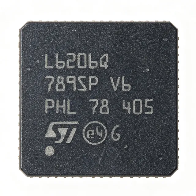
L6206Q - Dual DMOS Full-Bridge Driver 8A | STMicroelectronics
The STMicroelectronics L6206Q is a dual DMOS full-bridge motor driver capable of delivering up to 2.8A per channel (8A peak total) in a 48-pin QFN (QFN48) package. It operates from a supply voltage range of 8V to 52V, making it suitable for a wide variety of industrial and automotive motor control applications. The device integrates two independent H-bridges with a total output current of 5.6A continuous (2.8A per bridge), and includes thermal shutdown and undervoltage lockout protection. A DMOS full-bridge driver is a type of power integrated circuit that uses four N-channel DMOS transistors arranged in an H-bridge configuration to control the direction and speed of a DC motor or the phase currents of a stepper motor. It belongs to the broader category of motor drivers, which are power management ICs that translate low-power control signals into high-current, high-voltage outputs. The L6206Q sits in the hierarchy: DMOS full-bridge driver -> motor driver -> power management IC -> semiconductor. Key features include a low RDS(on) of 0.3 ohm per switch, which minimizes power dissipation and improves efficiency, and a fast switching frequency of up to 100 kHz, enabling precise PWM control. The device also features a non-dissipative overcurrent protection (OCP) that limits the output current to a safe level, and a diagnostic output that indicates fault conditions. The QFN48 package provides a compact footprint with an exposed thermal pad for enhanced heat dissipation. The L6206Q uses a mixed-signal BCD (Bipolar-CMOS-DMOS) process technology, integrating the DMOS power stage with CMOS control logic and bipolar protection circuits. This architecture allows for high current handling with low quiescent current and robust protection features. The device supports both parallel and bridge configurations, enabling flexible motor drive topologies. Typical applications include bipolar stepper motor drivers, DC motor drivers for robotics and automation, and brushless DC motor pre-drivers. The wide supply voltage range and high current capability make it ideal for industrial automation, CNC machines, and automotive actuators. In a stepper motor application, the L6206Q can drive two-phase motors with up to 2.8A per phase, providing smooth microstepping control. When designing with this device, ensure adequate PCB copper area for the thermal pad to dissipate heat, especially at high output currents. The VREF pin allows current sensing and regulation, which is essential for torque control in stepper applications. The EN pins provide independent enable control for each bridge, enabling power-saving modes. This page synthesizes distributor pricing, drop-in alternatives, and practical design notes not found in the ST datasheet, providing a comprehensive resource for engineers selecting a dual full-bridge driver.

L6207PD - DMOS Dual Full Bridge Motor Driver, 52V/2.8A | STMicroelectronics
The STMicroelectronics L6207PD is a DMOS dual full-bridge motor driver realized in MultiPower BCD technology, delivering up to 2.8 A continuous per bridge from an 8 V to 52 V supply in a PowerSO-36 slug-up package with exposed thermal pad. What is a DMOS dual full-bridge motor driver? It is an integrated power stage that contains four power DMOS transistors arranged as two complete H-bridges, plus on-chip logic and current-control circuitry, used to bidirectionally drive DC motors, stepper motors, or solenoids from a single supply rail. Within the broader product hierarchy, the L6207PD sits in the motor driver IC family, which belongs to power management semiconductors, a category that also includes voltage regulators, gate drivers, and motor controllers. Key features include a wide 8 V to 52 V operating supply range, 2.8 A continuous output current per bridge (with 5.6 A peak capability in PWM mode), on-chip dual independent constant-off-time PWM current controllers with programmable chopping, integrated non-dissipative overcurrent protection, thermal shutdown, and cross-conduction prevention logic. The BCD process combines isolated DMOS output transistors with CMOS and bipolar control circuitry on a single die, eliminating external gate-drive components and reducing PCB area. The DMOS output stage achieves low on-resistance RDS(on) of approximately 0.3 ohm per switch, which directly improves efficiency and reduces conduction losses compared with bipolar Darlingtons predecessors. The integrated dual PWM current controllers enable precise torque regulation in stepper motors by chopping the phase current at a user-defined threshold set via an external sense resistor and RC network, eliminating the need for an external microcontroller PWM loop. Typical applications include bipolar stepper motor drives, DC motor bidirectional control in industrial automation, positioning stages, and solenoid/valve drivers. The high 52 V supply tolerance also makes it suited for 24 V and 48 V industrial bus systems. The PowerSO-36 slug-up exposed pad package provides low thermal resistance, enabling continuous high-current operation with appropriate PCB copper area. When designing with this part, the user must provide sense resistors on the SENSE pins, set the OFF time through the RC pin, and observe the absolute maximum supply of 60 V. Heat sinking via PCB copper or an external heatsink on the slug-up tab is essential at currents above 1.5 A per bridge to maintain junction temperature within the 150 C limit.
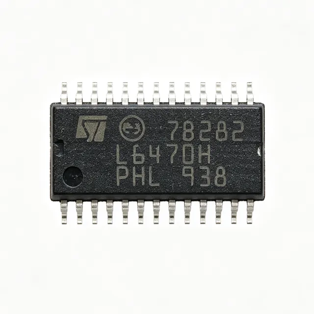
L6470H - dSPIN Stepper Motor Driver | STMicroelectronics | HTSSOP-28
The STMicroelectronics L6470H is a fully integrated microstepping motor driver with an embedded dSPIN™ motion engine, delivering up to 3 A peak output current per phase in a 28-pin HTSSOP (PowerSO-28) package. It operates from a supply voltage range of 8 V to 45 V and features programmable microstepping up to 1/128 step, making it suitable for high-resolution motion control applications. Data verified as of 2026-08-05. A stepper motor driver is a power management IC that translates digital step and direction commands into the precise current sequences needed to rotate a bipolar stepper motor. The L6470H belongs to the motor driver category, which sits within the broader power management IC hierarchy: motor driver -> power management IC -> semiconductor. Its integrated motion engine offloads complex acceleration and deceleration profiles from the host microcontroller, enabling smoother motion and reduced processor load. Key features include a programmable motor current from 0 mA to 3 A RMS, SPI interface for configuration and control, and a wide range of protection features such as overcurrent, overtemperature, and undervoltage lockout. The device also integrates a 1/128 microstepping capability, which significantly reduces motor noise and vibration compared to full-step operation. The HTSSOP-28 package with exposed pad provides excellent thermal performance, with a thermal resistance of 25 °C/W, enabling operation at high currents without external heatsinking in many applications. The L6470H uses a proprietary dSPIN™ architecture that combines a power stage, current sensing, and a motion profile generator on a single die. This integration reduces external component count and simplifies PCB layout. The SPI interface allows real-time adjustment of motor parameters, such as acceleration, deceleration, and target speed, enabling adaptive motion control in dynamic systems. The device also supports daisy-chaining of multiple drivers on a single SPI bus, simplifying multi-axis systems. Typical applications include 3D printers, CNC machines, robotics, and automated textile machinery. In a 3D printer, the L6470H's high microstepping resolution and quiet operation are critical for achieving precise layer deposition and reducing print artifacts. In robotics, the integrated motion engine allows smooth, controlled movement of joints and actuators, improving overall system performance. When designing with the L6470H, ensure adequate supply decoupling with a 100 nF ceramic capacitor close to the VSA and VSB pins, and a bulk capacitor (≥10 µF) on the supply rail. The exposed pad must be soldered to a large copper area for thermal management. The SPI lines should be kept short and shielded to avoid noise coupling into the motor current sense circuitry. This page synthesizes distributor pricing, drop-in alternatives, and practical design notes not found in the ST datasheet, providing engineers with a comprehensive resource for evaluating the L6470H in their motion control designs.

L6470HTR - dSPIN Stepper Motor Driver | STMicroelectronics
The L6470HTR is a fully integrated microstepping motor driver from STMicroelectronics, part of the dSPIN family. It combines a complete motor control system on a single chip, including a power stage with dual full-bridge drivers, a digital control core, and a serial interface. The device is designed to drive bipolar stepper motors with up to 3 A peak current per phase, operating from a supply voltage range of 8 V to 45 V. It is available in a compact HTSSOP28 package, making it suitable for space-constrained applications. A stepper motor driver is a power management IC that translates digital step and direction commands into the precise current sequences needed to rotate a stepper motor. The L6470HTR integrates the control logic, gate drivers, and power MOSFETs, eliminating the need for external components and simplifying PCB design. It belongs to the hierarchy: stepper motor driver -> motor driver -> power management IC -> semiconductor. This integration reduces system cost and board space while improving reliability. Key features of the L6470HTR include programmable microstepping up to 1/128 step, which provides smooth motion and high positioning accuracy. It offers a wide range of protection features, including overcurrent, overtemperature, and undervoltage lockout. The device also includes a SPI interface for configuration and control, allowing real-time adjustment of motor parameters. The integrated current sensing eliminates the need for external sense resistors, further reducing component count. The L6470HTR uses a proprietary control algorithm that automatically adjusts the current decay mode to optimize performance across different motor types and load conditions. This adaptive decay control minimizes audible noise and power dissipation. The device also features a programmable slew rate to reduce electromagnetic interference (EMI) in sensitive applications. The digital core operates at up to 16 MHz SPI clock, enabling fast communication with microcontrollers. Typical applications include 3D printers, CNC machines, robotics, office automation, and industrial automation. In 3D printers, the L6470HTR provides precise filament positioning with microstepping, resulting in high-quality prints. In CNC machines, it drives stepper motors for axis movement with high torque and accuracy. The device's wide voltage range and current capability make it versatile for various motor sizes. When designing with the L6470HTR, ensure proper thermal management by providing adequate copper area on the PCB for heat dissipation. The HTSSOP28 package has an exposed pad that must be soldered to a thermal relief. Additionally, place decoupling capacitors close to the power supply pins to minimize voltage transients. The SPI interface allows configuration of motor parameters, but careful attention to the register settings is required to avoid unintended behavior.