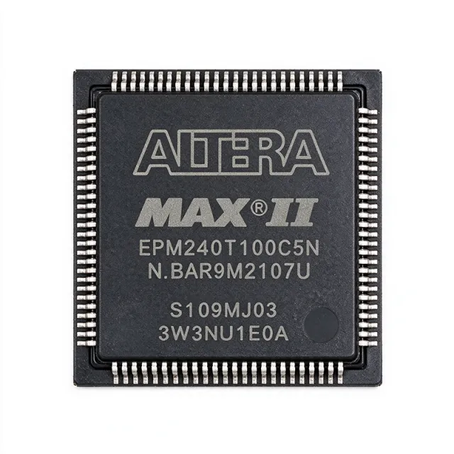
EPM240T100C5 - MAX II CPLD, 192 Macrocells, 100-TQFP | Altera
MPN: EPM240T100C5 ✓ Hoạt độngEPM240T100C5 Tóm tắt
A CPLD (Complex Programmable Logic Device) is a non-volatile programmable logic device that uses a macrocell-based architecture with continuous, distributed interconnect. In the system-level hierarchy, a CPLD sits below an FPGA (Field-Programmable Gate Array) in density, above small PAL/GAL devices, and below microcontroller units (MCUs) in flexibility. MAX II CPLDs target glue-logic, interface bridging, power-sequencing, and bus-management functions where deterministic timing and zero in-system configuration delay are mandatory.
Key features include 192 logic elements, 4.7 ns pin-to-pin logic delay (tPD1), 201.1 MHz maximum internal operating frequency, support for 2.5 V and 3.3 V core supply operation, MultiVolt I/O supporting 1.5 V/1.8 V/2.5 V/3.3 V levels, JTAG-based IEEE 1149.1 boundary-scan testing and in-system programmability (ISP), and a global chip-wide DEV_OE output enable pin for board-level tri-state control.
The device uses a non-volatile Flash-based architecture with 8 Kbits of embedded storage, four I/O banks for voltage-domain isolation, and on-chip pull-up resistors (User I/O pin 4 control) configurable in Quartus II. Each macrocell contains a programmable AND/OR array, a flip-flop, and feedback paths to the logic array, enabling compact state-machine and decoding-logic implementation.
Typical applications include I/O expansion for microcontrollers and microprocessors, address decoding and chip-select generation in memory subsystems, bus-interface bridging (LVCMOS, LVTTL, PCI-compatible), power-supply sequencing in multi-rail systems, and configurable glue logic in industrial automation equipment. The instant-on behavior also suits FPGA configuration control, where the CPLD provides boot-up housekeeping before the main FPGA completes its configuration cycle.
When designing with the EPM240T100C5, observe I/O bank voltage constraints: each of the four banks shares a common VCCIO that must match the signal level of devices connected to that bank. The 5.0-V tolerant I/O feature requires VCCIO at 3.3 V; do not apply 5 V to any I/O pin. Use Quartus II (legacy) or the Intel Quartus Prime Lite Edition for design entry, synthesis, and JTAG programming.
This page consolidates distributor pricing, verified specifications, and curated drop-in alternatives not found in the manufacturer datasheet alone, helping engineers evaluate EPM240T100C5 for both new designs and legacy upgrades from MAX 7000S or classic PLDs.
Bộ thay thế dễ dàng lắp đặt cho EPM240T100C5 — cùng gói, chân-to-chân tương thích. Các bộ phận yêu cầu hàn PCB bị loại trừ.
Các biến thể trong loạt này
Các mẫu cùng loạt có thể lắp đặt dễ dàng tương thích với EPM240T100C5 (cùng hình factor và footprint) — khác nhau ở Operating Temperature, Package, Process Technology, Programming Interface.
EPM240T100C5N
Liên hệ để biết giá
Xem tài liệu →EPM240T100C4N
Liên hệ để biết giá
Xem tài liệu →EPM240T100C4
Liên hệ để biết giá
Xem tài liệu →EPM240T100C3N
Liên hệ để biết giá
Xem tài liệu →EPM240GT100C5N
Liên hệ để biết giá
Xem tài liệu →EPM240GT100C5
Liên hệ để biết giá
Xem tài liệu →EPM240T100C5 Tỷ lệ tối đa & tính chất điện
| Family | MAX II |
| Device Type | CPLD (Complex Programmable Logic Device) |
| Macrocells | 192 |
| Maximum User I/O Pins | 80 |
| Logic Elements | 240 |
| Non-volatile Memory | 8 Kbits (embedded Flash) |
| Pin-to-Pin Logic Delay (tPD1) | 4.7 ns |
| Maximum Internal Frequency | 201.1 MHz |
| Process Technology | 0.18 µm, 6-layer metal Flash |
| Core Supply Voltage | 2.5 V / 3.3 V |
| I/O Voltage Support | 1.5 V / 1.8 V / 2.5 V / 3.3 V (MultiVolt I/O) |
| I/O Banks | 4 |
| Hộp | 100-pin TQFP (14 mm × 14 mm × 1 mm) |
| Programming Interface | JTAG (IEEE 1149.1) / ISP |
| Nhiệt độ hoạt động | 0C to +85C (Commercial) |
| Chip-wide Output Enable | DEV_OE pin |
Cấu hình chân EPM240T100C5
| Chân 1 | I/O — User I/O (Bank 1) |
| Chân 2 | I/O — User I/O (Bank 1) |
| Chân 3 | I/O — User I/O (Bank 1) |
| Chân 4 | I/O — User I/O (Bank 1) |
| Chân 5 | I/O — User I/O (Bank 1) |
| Chân 6 | VCCIO1 — Bank 1 I/O supply voltage |
| Chân 7 | I/O — User I/O (Bank 1) |
| Chân 8 | GND — Ground |
| Chân 9 | I/O — User I/O (Bank 1) |
| Chân 10 | I/O — User I/O (Bank 1) |
| Chân 11 | I/O — User I/O (Bank 1) |
| Chân 12 | I/O — User I/O (Bank 1) |
| Chân 13 | I/O — User I/O (Bank 1) |
| Chân 14 | I/O — User I/O (Bank 1) |
| Chân 15 | I/O — User I/O (Bank 1) |
| Chân 16 | VCCIO1 — Bank 1 I/O supply voltage |
| Chân 17 | I/O — User I/O (Bank 1) |
| Chân 18 | I/O — User I/O (Bank 1) |
| Chân 19 | I/O — User I/O (Bank 1) |
| Chân 20 | I/O — User I/O (Bank 1) |
| Chân 21 | I/O — User I/O (Bank 2) |
| Chân 22 | VCCIO2 — Bank 2 I/O supply voltage |
| Chân 23 | I/O — User I/O (Bank 2) |
| Chân 24 | GND — Ground |
| Chân 25 | I/O — User I/O (Bank 2) |
| Chân 26 | I/O — User I/O (Bank 2) |
| Chân 27 | I/O — User I/O (Bank 2) |
| Chân 28 | I/O — User I/O (Bank 2) |
| Chân 29 | I/O — User I/O (Bank 2) |
| Chân 30 | VCCIO2 — Bank 2 I/O supply voltage |
| Chân 31 | I/O — User I/O (Bank 2) |
| Chân 32 | I/O — User I/O (Bank 2) |
| Chân 33 | I/O — User I/O (Bank 2) |
| Chân 34 | I/O — User I/O (Bank 2) |
| Chân 35 | I/O — User I/O (Bank 2) |
| Chân 36 | I/O — User I/O (Bank 2) |
| Chân 37 | I/O — User I/O (Bank 2) |
| Chân 38 | VCCIO2 — Bank 2 I/O supply voltage |
| Chân 39 | I/O — User I/O (Bank 2) |
| Chân 40 | I/O — User I/O (Bank 2) |
| Chân 41 | GND — Ground |
| Chân 42 | I/O — User I/O (Bank 3) |
| Chân 43 | I/O — User I/O (Bank 3) |
| Chân 44 | VCCIO3 — Bank 3 I/O supply voltage |
| Chân 45 | I/O — User I/O (Bank 3) |
| Chân 46 | I/O — User I/O (Bank 3) |
| Chân 47 | I/O — User I/O (Bank 3) |
| Chân 48 | I/O — User I/O (Bank 3) |
| Chân 49 | I/O — User I/O (Bank 3) |
| Chân 50 | VCCIO3 — Bank 3 I/O supply voltage |
| Chân 51 | I/O — User I/O (Bank 3) |
| Chân 52 | I/O — User I/O (Bank 3) |
| Chân 53 | I/O — User I/O (Bank 3) |
| Chân 54 | I/O — User I/O (Bank 3) |
| Chân 55 | I/O — User I/O (Bank 3) |
| Chân 56 | I/O — User I/O (Bank 3) |
| Chân 57 | VCCIO3 — Bank 3 I/O supply voltage |
| Chân 58 | I/O — User I/O (Bank 3) |
| Chân 59 | I/O — User I/O (Bank 3) |
| Chân 60 | I/O — User I/O (Bank 3) |
| Chân 61 | GND — Ground |
| Chân 62 | I/O — User I/O (Bank 4) |
| Chân 63 | I/O — User I/O (Bank 4) |
| Chân 64 | VCCIO4 — Bank 4 I/O supply voltage |
| Chân 65 | I/O — User I/O (Bank 4) |
| Chân 66 | I/O — User I/O (Bank 4) |
| Chân 67 | I/O — User I/O (Bank 4) |
| Chân 68 | I/O — User I/O (Bank 4) |
| Chân 69 | I/O — User I/O (Bank 4) |
| Chân 70 | VCCIO4 — Bank 4 I/O supply voltage |
| Chân 71 | I/O — User I/O (Bank 4) |
| Chân 72 | I/O — User I/O (Bank 4) |
| Chân 73 | I/O — User I/O (Bank 4) |
| Chân 74 | I/O — User I/O (Bank 4) |
| Chân 75 | I/O — User I/O (Bank 4) |
| Chân 76 | I/O — User I/O (Bank 4) |
| Chân 77 | VCCIO4 — Bank 4 I/O supply voltage |
| Chân 78 | I/O — User I/O (Bank 4) |
| Chân 79 | I/O — User I/O (Bank 4) |
| Chân 80 | I/O — User I/O (Bank 4) |
| Chân 81 | GND — Ground |
| Chân 82 | DEV_OE — Chip-wide output enable (active high) |
| Chân 83 | I/O — User I/O (Bank 4) |
| Chân 84 | I/O — User I/O (Bank 4) |
| Chân 85 | TDI — JTAG Test Data In |
| Chân 86 | TMS — JTAG Test Mode Select |
| Chân 87 | TCK — JTAG Test Clock |
| Chân 88 | TDO — JTAG Test Data Out |
| Chân 89 | VCCINT — Core supply voltage (2.5 V or 3.3 V) |
| Chân 90 | GND — Ground |
| Chân 91 | I/O — User I/O (Bank 1) |
| Chân 92 | I/O — User I/O (Bank 1) |
| Chân 93 | I/O — User I/O (Bank 1) |
| Chân 94 | I/O — User I/O (Bank 1) |
| Chân 95 | I/O — User I/O (Bank 1) |
| Chân 96 | VCCIO1 — Bank 1 I/O supply voltage |
| Chân 97 | I/O — User I/O (Bank 1) |
| Chân 98 | I/O — User I/O (Bank 1) |
| Chân 99 | I/O — User I/O (Bank 1) |
| Chân 100 | I/O — User I/O (Bank 1) |
Ứng dụng tiêu biểu
EPM240T100C5 phù hợp cho 6 Áp dụngs: Microcontroller I/O Expansion and Glue Logic, Power Supply Sequencing in Multi-Rail Systems, FPGA Configuration and Boot Control, Bus Interface Bridging (LVCMOS, LVTTL, PCI), Industrial Automation Control Logic, Address Decoding in Memory Subsystems.
Microcontroller I/O Expansion and Glue Logic
The EPM240T100C5 expands a host MCU's limited GPIO by decoding address lines and generating chip-select strobes for peripherals like SRAM, Flash, and sensors. Its 192 macrocells and 80 user I/O pins provide ample headroom for 8-bit and 16-bit bus decoding, while the 4.7 ns pin-to-pin delay ensures address-to-CS propagation stays well under one 50 MHz system clock period. The instant-on non-volatile Flash eliminates boot-PROM overhead, so the CPLD is ready to drive chip-selects before the MCU finishes its PLL lock - critical for deterministic power-on behavior. Designers typically place the CPLD between the MCU EMI bus and 4-8 peripheral devices, freeing the MCU's GPIO for serial interfaces.
Được đề xuất
Power Supply Sequencing in Multi-Rail Systems
The EPM240T100C5 sequences 3-6 voltage rails (1.0 V core, 1.5 V DDR, 1.8 V I/O, 2.5 V PLLs, 3.3 V analog) in the correct order during power-up and reverse order during power-down. Each macrocell implements a comparator-and-counter state machine that watches a PGOOD signal and asserts the next rail's enable after a configurable delay. The non-volatile Flash means the sequencing logic is active within microseconds of VCCINT reaching 2.5 V, eliminating the race condition between bulk-capacitor charging and rail-monitors. Designers typically route 4 power-good inputs to the CPLD and 6 enable outputs to DC-DC converter PG pins.
Được đề xuất
FPGA Configuration and Boot Control
The EPM240T100C5 acts as a configuration controller for SRAM-based FPGAs that require multi-mode boot (JTAG / parallel / serial). It reads the FPGA's configuration mode-pins and drives them based on a user-defined mode sequence, holds the FPGA in RESET until VCCINT is stable, and generates the PROG_B pulse on demand. The 8 Kbit embedded Flash stores the mode-selection logic permanently, so no external PROM is needed. Designers route DONE, INIT_B, and CONFIG_B lines from the FPGA to the CPLD, with the CPLD returning CTRL0/CTRL1 selections. This pattern is common in industrial and telecom designs where field-upgrade flexibility is required.
Được đề xuất
Bus Interface Bridging (LVCMOS, LVTTL, PCI)
The EPM240T100C5 bridges between mismatched bus standards - for example, translating a 3.3 V LVCMOS microcontroller bus to 1.8 V LVCMOS peripherals or providing a 5-V-tolerant input buffer for legacy PCI signals (when VCCIO is set to 3.3 V). Four I/O banks allow voltage-domain isolation so 1.5 V, 1.8 V, 2.5 V, and 3.3 V devices can all connect to the same CPLD without external level-shifters. With 4.7 ns tPD, the bridge introduces negligible latency into memory-mapped interfaces. Typical designs use 8-16 macrocells per 8-bit bus-converter instance, leaving headroom for handshaking and parity logic.
Được đề xuất
Industrial Automation Control Logic
In factory-automation PLCs, distributed I/O blocks, and motor-control auxiliary boards, the EPM240T100C5 implements deterministic state machines for safety-interlock logic, encoder-decoder counting, and PWM-edge multiplexing. Its 0-85C commercial or -40-85C industrial variants and 4.7 ns tPD suit real-time control loops. The on-chip pull-up resistors (configurable per User I/O pin 4) reduce BOM cost by eliminating external 10K arrays. Designers typically deploy 1-2 CPLDs per PLC chassis to consolidate discrete logic that would otherwise require dozens of 74HC-series gates.
Được đề xuất
Address Decoding in Memory Subsystems
The EPM240T100C5 decodes 24-32 bit address lines into individual chip-selects for Flash, SRAM, DRAM, and peripheral registers in embedded systems. A typical implementation uses 32 macrocells to generate 8 chip-selects with address-range masking via internal feedback comparators. The instant-on behavior ensures the chip-selects are valid at the first clock edge after reset, eliminating the boot-window violation that occurs with SRAM-based FPGAs. Designers often combine this application with bus-cycle termination logic (RDY/BWAIT stretching) using the same CPLD, saving board area versus discrete MSI logic.
Được đề xuất
Tóm tắt các sản phẩm được đề xuất
Dữ liệu tham khảo kỹ thuật cho EPM240T100C5 — so sánh, hướng dẫn thiết kế và thông tin tuân thủ.
Hướng dẫn chọn lựa
So sánh với các sản phẩm thay thế
| Tham số | Sản phẩm này | EPM240T100C5N | EPM240T100C4N | EPM240T100C4 | EPM240T100C3N | EPM240GT100C5N | EPM240GT100C5 |
|---|---|---|---|---|---|---|---|
| Package | TQFP-100 | TQFP-100 - same | TQFP-100 - same | TQFP-100 - same | TQFP-100 - same | TQFP-100 - same | TQFP-100 - same |
| Brand | Altera (Intel) | Altera (Intel) | Altera (Intel) | Altera (Intel) | Altera (Intel) | Altera (Intel) | Altera (Intel) |
| Family | MAX II | MAX II | MAX II | MAX II | MAX II | MAX II G | MAX II G |
| Speed Grade | C5 (4.7 ns tPD) | C5 (4.7 ns tPD) | C4 (slower tPD) | C4 (slower tPD) | C3 (slowest tPD) | C5 | C5 |
| Lead-Free (RoHS) | No (leaded) | Yes (Pb-free) | Yes (Pb-free) | No (leaded) | Yes (Pb-free) | Yes (Pb-free) | No (leaded) |
| Macrocells | 192 | 192 | 192 | 192 | 192 | 192 | 192 |
| Non-volatile Flash | 8 Kbits | 8 Kbits | 8 Kbits | 8 Kbits | 8 Kbits | 8 Kbits | 8 Kbits |
| Core Voltage | 2.5 V / 3.3 V | 2.5 V / 3.3 V | 2.5 V / 3.3 V | 2.5 V / 3.3 V | 2.5 V / 3.3 V | 1.8 V / 2.5 V / 3.3 V | 1.8 V / 2.5 V / 3.3 V |
Bảo phân biệt quan trọng
- Faster speed grade than C4/C3 alternatives at identical footprint (vsEPM240T100C4N)
- Lower unit cost than MAX II G family with identical macrocell count (vsEPM240GT100C5N)
- Leaded (SnPb) finish for legacy / non-RoHS assembly (vsEPM240T100C5N)
Ghi chú thiết kế
Decouple each VCCINT and VCCIO pin with a 0.1 µF ceramic capacitor placed within 5 mm of the respective pin and a 10 µF bulk tantalum or ceramic capacitor at the board-level supply rail. The four VCCIO banks allow mixed-voltage operation (1.5 V / 1.8 V / 2.5 V / 3.3 V) but each bank must share a common voltage; do not drive signals between different VCCIO domains without series resistors or level shifters if voltage mismatch exceeds 0.3 V.
The 100-pin TQFP has a 0.5 mm pitch and 14 mm × 14 mm body - use 4-mil (0.1 mm) traces between pads with 8-mil (0.2 mm) clearance for escape routing. Place a continuous ground plane on the layer directly beneath the device to minimize ground bounce on the JTAG and DEV_OE pins. Route JTAG signals (TDI, TMS, TCK, TDO) in a daisy-chain with 10K pull-ups on TDI/TMS/TCK as recommended in the MAX II handbook.
When using the EPM240T100C5 for high-speed address decoding or bus-bridging, observe 50 ohm controlled-impedance routing on outputs driving more than 25 mm of trace. Source-synchronous clocks should be assigned to dedicated clock input pins and use the on-chip PLL-free global clock network - the MAX II does not contain a PLL, so clock multiplication must be implemented in the macrocell fabric. Add 22-33 ohm series damping resistors on outputs driving backplane connectors to suppress ringing.
Do not apply 5.0 V to any I/O pin when VCCIO is set to less than 3.3 V - the absolute-maximum VCCIO+0.3 V input rating applies, and 5 V tolerance requires VCCIO = 3.3 V. Do not leave JTAG pins floating during in-system operation; floating TMS or TCK can inadvertently trigger boundary-scan operations. Verify that the Quartus II .pof programming file matches the target device ID before JTAG programming - using a C5 image on a C4 device will fail verification.
Thông tin tuân thủ
EPM240T100C5 is leaded (SnPb finish) and not RoHS compliant. For RoHS-compliant production, use the EPM240T100C5N variant. AEC-Q100 qualification does not apply (commercial temperature range 0-85C). Industrial -40-85C variant is EPM240T100I5N.







