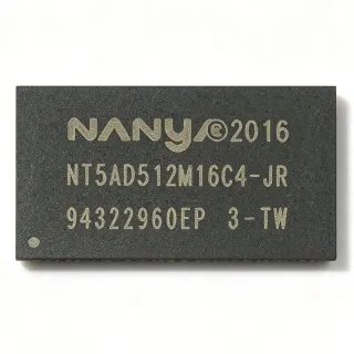
H58G46AK6PX033N - LPDDR5 16Gb 6400Mbps Automotive DRAM | SK hynix
MPN: H58G46AK6PX033N ✓ Hoạt độngH58G46AK6PX033N Tóm tắt
LPDDR5 (Low Power Double Data Rate 5) is a JEDEC-standardized mobile and automotive memory interface belonging to the DRAM hierarchy: LPDDR5 -> SDRAM -> DRAM -> semiconductor memory IC. Compared with DDR4/DDR5, LPDDR5 optimizes power efficiency with lower I/O swing and deep power-down states, making it the dominant volatile memory for battery-powered and thermally constrained platforms, including automotive ADAS domain controllers.
Key features of the H58G46AK6PX033 include the 6400 Mbps pin speed (LPDDR5-6400 class), a 16Gb density organized as x16, and automotive qualification for extended-reliability deployments such as infotainment, telematics, and ADAS memory subsystems. SK hynix LPDDR5 also implements bank-group architecture, on-die termination refinements, and a WCK clocking scheme that sustains high effective bandwidth at low power. The 315-ball FBGA footprint supports compact PCB layouts typical of compute modules and system-on-module designs.
Architecturally, the device uses the LPDDR5 16b-channel style command/data interface with dual WCK clocks, DQS strobes per byte lane, and programmable drive strength. The 1.8V/1.05V/0.5V triple-rail scheme separates interface power from core power, enabling DVFS power management by the host memory controller.
Typical applications include automotive ADAS domain controllers, digital cockpits and infotainment SoCs, industrial computing modules, edge AI accelerators, and high-performance mobile/consumer computing systems requiring 2GB LPDDR5 per component.
Design consideration: verify the host SoC memory controller supports LPDDR5-6400 timing and that the 315-ball routing follows SK hynix length-matching and reference-plane guidance in the manufacturer datasheet.
This page synthesizes verified distributor listings, drop-in alternative analysis, and procurement guidance not consolidated in the manufacturer datasheet.
Bộ thay thế dễ dàng lắp đặt cho H58G46AK6PX033N — cùng gói, chân-to-chân tương thích. Các bộ phận yêu cầu hàn PCB bị loại trừ.
Các biến thể trong loạt này
Các mẫu cùng loạt có thể lắp đặt dễ dàng tương thích với H58G46AK6PX033N (cùng hình factor và footprint) — khác nhau ở Memory Type, Organization, Density, Application Domain, Interface.
H58G46AK6PX033
✅ Drop-InLiên hệ để biết giá
Xem tài liệu →H58G46BK6PX033
✅ Drop-In ⚠️ Thông số chưa được xác minh📋 Tham chiếu thay thế (không có trong danh mục)
H58G46AK6PX033N Thông số kỹ thuật
| Kiểu bộ nhớ | LPDDR5 SDRAM |
| Density | 16 Gb (2 GB) |
| Tổ chức | x16 |
| Tốc độ dữ liệu | 6400 Mbps/pin |
| Interface Standard | JEDEC LPDDR5 |
| VDD2 Supply Voltage | 1.8 V |
| VDDQ Supply Voltage | 1.05 V |
| VDD1 (Core) Supply Voltage | 0.5 V |
| Hộp | 315-ball FBGA |
| Kiểu lắp đặt | Surface Mount (BGA) |
| Grade | Automotive |
| Application Domain | Mobile, automotive, industrial controllers, computing modules |
Hướng dẫn cấu hình chân H58G46AK6PX033N 315-ball fbga
Cấu hình chân cho H58G46AK6PX033N (315-ball fbga gói). Số thứ tự chân, chức năng và sơ đồ kết nối được xác định trong tài liệu thông số kỹ thuật của nhà sản xuất. Tham khảo nó để biết footprint và hướng dẫn hàn chính xác.

Không có dữ liệu chân cụ thể sẵn có cho H58G46AK6PX033N.
Tham khảo: tài liệu kỹ thuật cho cấu hình chân đầy đủ.
Ứng dụng tiêu biểu
H58G46AK6PX033N phù hợp cho 6 Áp dụngs: Automotive ADAS Domain Controllers, Digital Cockpit and Infotainment, Edge AI Accelerator Modules, Industrial Computing Modules, Mobile and Consumer Computing, Telematics and Embedded Logging.
Automotive ADAS Domain Controllers
The H58G46AK6PX033N fits ADAS domain controllers because its 6400 Mbps/pin LPDDR5 interface delivers roughly 12.8 GB/s of peak bandwidth per component at a x16 bus width - the throughput needed to stream camera, radar, and lidar sensor data into CNN-based perception pipelines. Its automotive qualification targets the extended reliability and quality expectations of vehicle platforms, and the 2GB capacity supports frame buffering plus intermediate feature maps for multi-sensor fusion. In the memory subsystem, the component is soldered to the 315-ball FBGA footprint on a length-matched fly-by or point-to-point route to the host SoC's LPDDR5 controller, with WCK clocking and per-byte DQS strobes. The 1.05V VDDQ rail keeps I/O power low, an important consideration for thermally sealed automotive enclosures with no active cooling.
Được đề xuất
Digital Cockpit and Infotainment
Digital cockpit SoCs drive multiple high-resolution displays and require memory bandwidth that scales with pixel throughput; the H58G46AK6PX033N's LPDDR5-6400 interface supplies approximately 12.8 GB/s per component, enough to sustain multi-display rendering plus navigation map streaming without starving the GPU. The 16Gb (2GB) density suits mid-tier cockpit platforms where several components are paired to reach 4GB-8GB total. Its automotive grade matches the cockpit's in-vehicle deployment requirements, while the 0.5V core rail and LPDDR5 power-down states reduce standby draw during ignition-off states - a key constraint for battery-protective sleep budgets. Layout-wise, the 315-ball FBGA is placed adjacent to the cockpit SoC with strict length matching on the data groups; the 1.8V VDD2 rail should be decoupled per SK hynix reference designs to suppress transients during display refresh bursts.
Được đề xuất
Edge AI Accelerator Modules
Edge AI inference modules need high memory bandwidth in a small, power-limited envelope, and the H58G46AK6PX033N addresses exactly this: 6400 Mbps/pin over x16 gives 12.8 GB/s of bandwidth per component while LPDDR5's low 1.05V I/O swing minimizes switching power versus legacy interfaces. System designers populate two to four components beside the AI SoC to form a 4GB-8GB bank, sufficient for quantized vision and audio models with workspace buffers. The 315-ball FBGA allows stacked, near-die placement that shortens traces and improves signal integrity at 6400 Mbps. Because the device is automotive qualified, the same module design can be reused across consumer and vehicle edge-AI products. Thermal design should account for DRAM self-refresh and active-access power under sustained inference loads, typically managed with via-array heat spreading into the module PCB.
Được đề xuất
Industrial Computing Modules
Industrial controllers and compute modules (COM Express, SMARC form factors) embed soldered LPDDR5 to eliminate connector reliability issues in vibration-heavy environments, and the H58G46AK6PX033N's automotive-qualified build exceeds typical industrial robustness expectations. Its 2GB-per-component density and 6400 Mbps rate let a 4GB module configuration serve machine-vision inspection, robotics control, and protocol-gateway workloads with headroom for containerized runtime stacks. The triple-rail scheme (1.8V / 1.05V / 0.5V) integrates cleanly with module power trees that already generate 1.8V and 1.05V rails for other silicon. During design, the module vendor should follow SK hynix's 315-ball FBGA routing guidance - controlled-impedance data groups, WCK length matching, and solid reference planes - to sustain 6400 Mbps signaling across the module connector's indirectly referenced environment.
Được đề xuất
Mobile and Consumer Computing
In smartphones, tablets, and consumer compute devices, LPDDR5 is the dominant main-memory interface because it maximizes bandwidth per watt; the H58G46AK6PX033N provides 16Gb per component with 6400 Mbps/pin, so two to four packages deliver 4GB-8GB of RAM - the typical mid-range configuration. LPDDR5 power-management features (per-bank refresh, deep sleep modes) extend standby battery life, which is the primary differentiator versus DDR4/DDR5 in this segment. The 315-ball FBGA's fine pitch supports the compact PoP-adjacent layouts of mobile PCBs. Consumer designs without automotive requirements can also consider the same silicon in non-automotive ordering options within the H58G46AK6 family to optimize cost. Signal integrity at 6400 Mbps demands strict stackup control: 4+ layer PCBs with impedance-controlled traces and per-byte DQS tuning during controller training are standard practice.
Được đề xuất
Telematics and Embedded Logging
Telematics control units and embedded data-logging platforms use the H58G46AK6PX033N as working memory for OTA update staging, V2X protocol stacks, and buffered sensor logging before writes to flash. The LPDDR5-6400 interface provides responsive random-access performance for protocol processing, while the 2GB capacity holds simultaneous navigation, connectivity, and logging workloads. Automotive qualification is essential here because telematics units remain powered across wide ambient temperature swings and must survive crank/partial-power conditions. Designers typically pair the DRAM with an automotive SPI NOR or NAND for persistent storage and place the 315-ball FBGA close to the telematics SoC with the 1.8V VDD2 and 1.05V VDDQ rails sequenced per the power-up requirements in the SK hynix datasheet to avoid latch-up during ignition transients.
Được đề xuất
Tóm tắt các sản phẩm được đề xuất
Dữ liệu tham khảo kỹ thuật cho H58G46AK6PX033N — so sánh, hướng dẫn thiết kế và thông tin tuân thủ.
Hướng dẫn chọn lựa
So sánh với các sản phẩm thay thế
| Tham số | Sản phẩm này | H58G46AK6PX033 | H58G46BK6PX033 |
|---|---|---|---|
| Package | 315-ball FBGA | 315-ball FBGA - same | 315-ball FBGA - same |
| Brand | SK hynix | SK hynix | SK hynix |
| Density | 16 Gb (2 GB) | 16 Gb (2 GB) | 16 Gb (2 GB) |
| Organization | x16 | x16 | x16 |
| Data Rate | 6400 Mbps/pin | 6400 Mbps/pin | 6400 Mbps/pin |
| Interface Standard | JEDEC LPDDR5 | JEDEC LPDDR5 | JEDEC LPDDR5 |
| Supply Rails | 1.8 V / 1.05 V / 0.5 V | 1.8 V / 1.05 V / 0.5 V | 1.8 V / 1.05 V / 0.5 V |
| Ordering Suffix Meaning | N = packaging/flow ordering variant | base part number | B-family revision code |
Bảo phân biệt quan trọng
- Identical silicon in base part number (vsH58G46AK6PX033)
- Automotive qualification vs consumer LPDDR5 (vsGeneric consumer LPDDR5 components)
- LPDDR5-6400 bandwidth efficiency (vsDDR4 automotive parts (e.g., H5CG46AGBDX015))
Ghi chú thiết kế
Route the LPDDR5-6400 interface with controlled impedance (approximately 40 ohm single-ended for data groups per typical LPDDR5 practice) and keep all data-group traces length-matched within the window specified in the SK hynix datasheet. Place the H58G46AK6PX033N 315-ball FBGA as close to the host SoC as the fanout allows; every millimeter of trace at 6400 Mbps increases ISI and reflection risk. Maintain solid, unbroken reference planes under all DQ/DM/DQS nets and avoid crossing plane splits.
The device requires three rails - 1.8V (VDD2), 1.05V (VDDQ), and 0.5V (VDD1 core). Sequence power-up per the SK hynix datasheet order and decouple each rail with a network of bulk plus 0.1uF/0.01uF ceramics placed at the ball escapes. The 0.5V core rail carries the highest transient current during burst accesses; size the DC-DC converter with margin and verify rail droop during controller training patterns.
Do not assume cross-brand LPDDR5 parts are drop-in: ball maps and mode-register initialization differ between SK hynix and Micron even at matched density and speed. Always re-run memory controller training and boot-time validation after any substitution, and confirm the ordering suffix (the N in H58G46AK6PX033N) matches your packaging requirement in the SK hynix ordering information table before release to production.
Thông tin tuân thủ
Verified data identifies the part as automotive-grade, but specific RoHS/REACH/AEC-Q100 qualification statements were not present in the provided data.