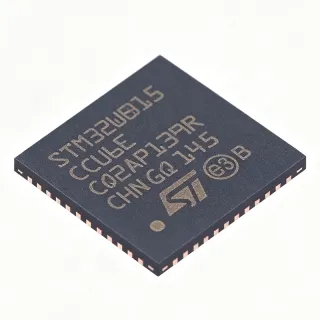
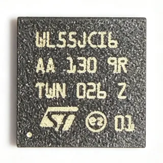
NRF51822QFAC - Bluetooth LE/2.4GHz SoC, 256kB Flash | Nordic
MPN: NRF51822QFAC ✗ Cuối đờiNRF51822QFAC Tóm tắt
An RF System-on-Chip (SoC) is a single silicon die that combines a microcontroller core, on-chip program and data memory, analog/RF peripherals, and a radio transceiver. The nRF51822 belongs to the Bluetooth SoC family (Bluetooth low energy SoC -> wireless MCU -> connected microcontroller -> general-purpose MCU), which is itself a branch of the broader category of short-range wireless ICs. By collapsing the MCU and radio into one die, an RF SoC dramatically shrinks PCB area, simplifies BOM, and lowers sleep current compared with two-chip MCU+transceiver designs - enabling coin-cell-powered products that can run for years on a single CR2032.
Key features include a Cortex-M0 core running up to 16 MHz (31.25 MHz when using the on-chip HFCL), 256 kB on-chip flash for application + softdevice storage, 32 kB on-chip SRAM, a flexible 2.4 GHz radio supporting Bluetooth low energy (v4.0) and Nordic Gazell proprietary modes, integrated balun, and a rich set of peripherals including 10-bit ADC, RTC, GPIO, I2C, SPI, UART, and PWM. The QFN-48 (6x6 mm) package exposes an EP that must be soldered to the board ground for thermal and RF performance.
Typical applications include BLE beacons, fitness bands, smart watches, medical sensor patches, remote controls, smart-home bridges, and industrial telemetry nodes. The combination of sub-uA sleep current and on-chip Cortex-M0 processing makes it well suited to products where battery life is measured in months rather than hours.
When laying out a board, observe Nordic's reference layout: route the differential RF port (RFIO P0.18 / RFIO1 P0.21 on QFACA) with controlled 50 ohm impedance, place the chip's exposed pad on a continuous ground pour, and keep decoupling capacitors within 2 mm of the supply pins. The radio's TX output power, RX sensitivity, and blocking performance all depend on this layout.
This page synthesizes distributor pricing, drop-in QFN-48 alternatives from the Nordic nRF51/nRF52 family, and PCB-level design notes that are not collected in any single manufacturer document.
Bộ thay thế dễ dàng lắp đặt cho NRF51822QFAC — cùng gói, chân-to-chân tương thích. Các bộ phận yêu cầu hàn PCB bị loại trừ.
NRF51822QFAC-R
✅ Drop-In📋 Tham chiếu thay thế (không có trong danh mục)
NRF51822QFAC-T
✅ Drop-In📋 Tham chiếu thay thế (không có trong danh mục)
NRF51822QFAA-R
✅ Drop-In📋 Tham chiếu thay thế (không có trong danh mục)
NRF51422QFAC
✅ Drop-In📋 Tham chiếu thay thế (không có trong danh mục)
NRF52832QFAA
✅ Drop-In📋 Tham chiếu thay thế (không có trong danh mục)
NRF51822QFAC Tỷ lệ tối đa & tính chất điện
| Product Type | Bluetooth Low Energy / 2.4 GHz SoC |
| Core | ARM Cortex-M0 |
| Core Clock | 16 MHz (HFCL 31.25 MHz available) |
| Flash | 256 kB |
| RAM | 32 kB |
| Radio | 2.4 GHz Bluetooth v4.0 + proprietary (Gazell) |
| Hộp | 48-pin QFN (6 x 6 mm) with exposed pad (QFN-48 / 48-VFQFN-EP) |
| Kiểu lắp đặt | Surface Mount |
| Peripherals | 10-bit ADC, RTC, I2C, SPI, UART, PWM, AES |
| Protocol Stack | Bluetooth low energy (v4.0), 2.4 GHz Gazell |
| Trạng thái RoHS | Compliant |
| Lead-Free | Yes |
Cấu hình chân NRF51822QFAC
| Chân 1 | VDD — Power supply input |
| Chân 2 | GND — Ground |
| Chân 3 | DEC1 — Decoupling pin |
| Chân 4 | DEC2 — Decoupling pin |
| Chân 5 | DEC3 — Decoupling pin |
| Chân 6 | DEC4 — Decoupling pin |
| Chân 7 | VDDH — High-voltage supply (radio) |
| Chân 8 | VDD_PA — Power amplifier supply |
| Chân 9 | ANT — Differential antenna port (P0.18 / ANT1) |
| Chân 10 | ANT2 — Differential antenna port (P0.21 / ANT2) |
| Chân 11 | GND — Ground |
| Chân 12 | RESET — Reset pin (active low) |
| Chân 13 | SWDIO — Serial Wire Debug I/O |
| Chân 14 | SWDCLK — Serial Wire Debug clock |
| Chân 15 | GPIO — General purpose I/O |
| Chân 16 | GPIO — General purpose I/O |
| Chân 17 | GPIO — General purpose I/O |
| Chân 18 | GPIO — General purpose I/O |
| Chân 19 | GPIO — General purpose I/O |
| Chân 20 | GPIO — General purpose I/O |
| Chân 21 | GPIO — General purpose I/O |
| Chân 22 | GPIO — General purpose I/O |
| Chân 23 | GPIO — General purpose I/O |
| Chân 24 | GPIO — General purpose I/O |
| Chân 25 | GPIO — General purpose I/O |
| Chân 26 | GPIO — General purpose I/O |
| Chân 27 | GPIO — General purpose I/O |
| Chân 28 | GPIO — General purpose I/O |
| Chân 29 | GPIO — General purpose I/O |
| Chân 30 | GPIO — General purpose I/O |
| Chân 31 | GPIO — General purpose I/O |
| Chân 32 | GPIO — General purpose I/O |
| Chân 33 | GPIO — General purpose I/O |
| Chân 34 | GPIO — General purpose I/O |
| Chân 35 | GPIO — General purpose I/O |
| Chân 36 | GPIO — General purpose I/O |
| Chân 37 | GPIO — General purpose I/O |
| Chân 38 | GPIO — General purpose I/O |
| Chân 39 | GPIO — General purpose I/O |
| Chân 40 | GPIO — General purpose I/O |
| Chân 41 | GPIO — General purpose I/O |
| Chân 42 | GPIO — General purpose I/O |
| Chân 43 | DEC5 — Decoupling pin |
| Chân 44 | DEC6 — Decoupling pin |
| Chân 45 | VDD — Power supply input |
| Chân 46 | GND — Ground |
| Chân 47 | GND — Ground |
| Chân 48 | GND — Ground |
Ứng dụng tiêu biểu
NRF51822QFAC phù hợp cho 7 Áp dụngs: Bluetooth Low Energy Beacons, Fitness Bands and Wearables, Medical Sensor Patches, Smart Home Hubs and Bridges, Industrial Wireless Sensor Nodes, BLE-Enabled Remote Controls, Wireless PC Peripherals (Mice/Keyboards).
Bluetooth Low Energy Beacons
The NRF51822QFAC's 256 kB flash comfortably fits Eddystone or iBeacon firmware alongside the BLE softdevice, while its sub-microamp sleep current lets coin-cell-powered beacons advertise for 1-3 years on a single CR2032. Place the chip with its exposed pad soldered to a continuous ground pour to preserve the radio link budget - the QFN-48 footprint is small enough to fit inside a 25 mm diameter puck-style beacon enclosure.
Được đề xuất
Fitness Bands and Wearables
With Cortex-M0 DSP plus BLE v4.0, the NRF51822QFAC can drive a fitness band's accelerometer, heart-rate sensor, and OLED display while streaming data to a smartphone over BLE. The 256 kB flash and 32 kB RAM are sufficient for typical wearable application code. The QFN-48 6x6 mm footprint fits inside a 15 mm x 40 mm band module, and the BLE link enables real-time heart-rate broadcast and firmware updates over the air (DFU).
Được đề xuất
Medical Sensor Patches
Medical patch designs leverage the NRF51822QFAC's ultra-low sleep current and Cortex-M0 processing to drive continuous glucose, temperature, or ECG monitoring from a 3V coin cell. The integrated AES hardware accelerator enables secure BLE communication required for HIPAA-conscious medical data transfer. Use an external LDO like the LP5900TLX-1.8 to clean the supply for low-noise analog front-end measurements.
Được đề xuất
Smart Home Hubs and Bridges
In a smart-home bridge, the NRF51822QFAC's BLE radio and Cortex-M0 can act as a gateway between BLE sensors and a Wi-Fi/Ethernet host. The 256 kB flash supports the BLE softdevice plus a Gazell proprietary bridge protocol for legacy 2.4 GHz sensors. The QFN-48 footprint is small enough to embed inside a wall-switch module, and Nordic's Gazell star network lets the hub pair with up to 8000 sensor nodes.
Được đề xuất
Industrial Wireless Sensor Nodes
Industrial sensor nodes benefit from the NRF51822QFAC's industrial temperature range and robust 2.4 GHz radio. Combined with Modbus-over-BLE firmware, the chip can wirelessly expose factory sensor data to a tablet or gateway. The exposed-pad QFN-48 package is suitable for conformal-coated industrial boards, and Nordic's OTA DFU capability allows remote firmware updates across thousands of deployed nodes.
Được đề xuất
BLE-Enabled Remote Controls
TV set-top boxes, smart speakers, and BLE remote controls use the NRF51822QFAC for voice command relay, BLE pairing, and IR-over-BLE bridges. Its 256 kB flash supports rich HID profiles plus voice codec buffering. Pair it with a low-power audio ADC and a haptic driver to create a full-featured BLE remote that runs for over a year on two AAA batteries thanks to the chip's low sleep current.
Được đề xuất
Wireless PC Peripherals (Mice/Keyboards)
The NRF51822QFAC's BLE v4.0 radio and 2.4 GHz proprietary mode are widely used in low-latency wireless mice, keyboards, and game controllers. Nordic's Gazell mode offers sub-5 ms latency suitable for gaming mice, while BLE enables universal smartphone pairing. The chip's high GPIO count drives a 16-bit RGB LED matrix and a high-resolution scroll-wheel sensor simultaneously.
Được đề xuất
Tóm tắt các sản phẩm được đề xuất
Dữ liệu tham khảo kỹ thuật cho NRF51822QFAC — so sánh, hướng dẫn thiết kế và thông tin tuân thủ.
Hướng dẫn chọn lựa
So sánh với các sản phẩm thay thế
| Tham số | Sản phẩm này | NRF51822QFAC-R | NRF51822QFAC-T | NRF51822QFAA-R | NRF51422QFAC | NRF52832QFAA |
|---|---|---|---|---|---|---|
| Brand | Nordic Semiconductor | Nordic Semiconductor | Nordic Semiconductor | Nordic Semiconductor | Nordic Semiconductor | Nordic Semiconductor |
| Package | QFN-48 (6x6 mm) | QFN-48 (6x6 mm) - same | QFN-48 (6x6 mm) - same | QFN-48 (6x6 mm) - same | QFN-48 (6x6 mm) - same | QFN-48 (6x6 mm) - same |
| Core | ARM Cortex-M0 | ARM Cortex-M0 | ARM Cortex-M0 | ARM Cortex-M0 | ARM Cortex-M0 | ARM Cortex-M3A |
| Flash | 256 kB | 256 kB | 256 kB | 128 kB | 256 kB | 512 kB |
| RAM | 32 kB | 32 kB | 32 kB | 16 kB | 32 kB | 64 kB |
| Bluetooth Version | v4.0 BLE | v4.0 BLE | v4.0 BLE | v4.0 BLE | v4.0 BLE + ANT+ | Bluetooth 5 |
| ANT+ Support | No | No | No | No | Yes | No |
| Lifecycle Status | NRND | NRND | NRND | NRND | NRND | Active |
Bảo phân biệt quan trọng
- Highest on-chip memory in nRF51822 family (vsNRF51822QFAA-R)
- Lower-power Cortex-M0 vs newer Cortex-M3A core (vsNRF52832QFAA)
- Pin-compatible upgrade path to active-production nRF52832 (vsNRF52832QFAA)
Ghi chú thiết kế
Route the differential RF port (ANT/ANT2 on the QFN-48 QFAC build) with a controlled 50 ohm differential impedance. Nordic's reference layout shows a 0.5 mm trace width on 0.2 mm spacing over a 4-layer FR4 stackup. The exposed pad (EP) must be soldered to a continuous ground plane with at least 8 thermal vias - omitting the EP ground connection degrades radio range and causes RF instability.
Decouple each VDD/VDDH pin with a 100 nF ceramic capacitor placed within 2 mm of the pin. Add a 10 uF bulk capacitor near the radio section to absorb TX load transients (peak current ~12 mA at 0 dBm). A separate LP5029 ferrite bead between the digital and RF supplies reduces conducted noise coupling into the ADC readings.
Do not assume the QFAC variant has the same pinout as QFAA builds across all GPIO assignments - several pin functions (e.g. RESET, SWDIO) move between QFAC/QFAA revisions. Always cross-reference the exact pin name table in the nRF51822 datasheet before PCB layout. Failing to do so results in non-functional boards that pass initial power-up but fail firmware download.
At maximum continuous TX output (0 dBm), the QFN-48 die dissipates roughly 30 mW. With the EP soldered to a 1 square inch copper pour on a 4-layer board, theta_JA is around 35 C/W, yielding a 1 C temperature rise above ambient - acceptable. Without the EP ground, junction temperature can rise 10-15 C, risking CW transmission failures above 25 C ambient.
Thông tin tuân thủ
RoHS and REACH compliant per Nordic product page. Not AEC-Q100 qualified - this part is intended for consumer/commercial/industrial wireless products, not automotive. Conflict-minerals declaration available from Nordic.