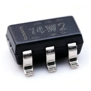
OPA335AIDBVR - Zero-Drift 5uV Op Amp, 2MHz, SOT-23-5 | TI
MPN: OPA335AIDBVR ✓ Hoạt độngOPA335AIDBVR Tóm tắt
A zero-drift operational amplifier is a type of precision analog amplifier that uses internal auto-zeroing or chopper-stabilization techniques to continuously cancel the input-offset voltage and its variation with temperature. Within the broader signal-chain hierarchy, an op amp functions as the fundamental active building block for amplification, filtering, and signal translation; precision zero-drift variants sit at the top of that taxonomy (precision op amp -> operational amplifier -> amplifier -> analog IC -> semiconductor). Compared to conventional CMOS op amps whose offset can drift tens of microvolts over temperature, the OPA335 holds sub-microvolt drift over the full -40C to +125C range, eliminating periodic calibration in many instrumentation paths.
Key features include 285 uA typical quiescent current, 2 kV HBM ESD on the input pins, unity-gain stable operation with 1 nF capacitive loads, and rail-to-rail output that swings within 30 mV of either supply at 10 kohm loading. The TI proprietary auto-zero architecture produces no chopping artifacts in the audio band, allowing clean thermopile and strain-gauge signal chains. Internal RFI/EMI rejection filtering at the inputs suppresses out-of-band interference from cellular, Wi-Fi, or motor-drive sources without external RC networks.
The OPA335 pairs an internal precision oscillator with switched-capacitor nulling to dynamically measure and correct offset every clock cycle. This architecture removes the 1/f noise that dominates low-frequency CMOS amplifiers and creates a flat noise spectral density down to DC. Because the device operates from a single supply, designers can omit the negative rail that traditional bipolar precision amplifiers require, saving PCB area and BOM cost.
Typical applications include thermocouple and RTD front-ends, load-cell conditioning for weighing scales, precision current sensing for battery monitors, medical instrumentation such as glucose meters, and handheld industrial test equipment. The 2.7 V minimum supply also enables direct 3.3 V system integration with MCUs and ADCs.
When laying out the OPA335, keep input traces short and guarded, route the high-impedance nodes away from switching nodes, and place the 0.1 uF supply bypass within 3 mm of the V+ pin. Designers should avoid placing large capacitive loads directly at the output - the amplifier remains stable with up to 1 nF but rapidly loses phase margin above that.
This page synthesizes distributor pricing, drop-in SOT-23-5 alternatives, and practical layout notes from the manufacturer datasheet, providing comparison and selection context not available on a single-line distributor listing.
Bộ thay thế dễ dàng lắp đặt cho OPA335AIDBVR — cùng gói, chân-to-chân tương thích. Các bộ phận yêu cầu hàn PCB bị loại trừ.
Các biến thể trong loạt này
Các mẫu cùng loạt có thể lắp đặt dễ dàng tương thích với OPA335AIDBVR (cùng hình factor và footprint) — khác nhau ở Amplifier Type, Operating Temperature Range, Package, Slew Rate.
OPA334AIDBVR
✅ Drop-In📋 Tham chiếu thay thế (không có trong danh mục)
OPA330AIDBVR
✅ Drop-In📋 Tham chiếu thay thế (không có trong danh mục)
OPA335AIDBVT
✅ Drop-In📋 Tham chiếu thay thế (không có trong danh mục)
OPA335AID
✅ Drop-In ⚠️ Thông số chưa được xác minh📋 Tham chiếu thay thế (không có trong danh mục)
AD8628ARTZ-REEL7
✅ Drop-InLiên hệ để biết giá
Xem tài liệu →MAX44260AUD+T
✅ Drop-In📋 Tham chiếu thay thế (không có trong danh mục)
OPA335AIDBVR Tỷ lệ tối đa & tính chất điện
| Amplifier Type | Zero-Drift, Precision, Auto-Zero |
| Number of Channels | 1 |
| Maximum Offset Voltage (VOS) | 5 uV (at 25C) |
| Maximum Offset Voltage Drift (dVOS/dT) | 0.05 uV/C |
| Gain-Bandwidth Product (GBW) | 2 MHz |
| Slew Rate | 1.6 V/us |
| Supply Voltage Range (Single Supply) | 2.7 V to 5.5 V |
| Quiescent Current (IQ) | 285 uA typical |
| Kiểu đầu ra | Rail-to-Rail Output |
| Output Swing (10 kohm load) | Within 30 mV of either rail |
| Khoảng nhiệt độ hoạt động | -40C to +125C |
| ESD Rating (HBM) | 2 kV |
| Shutdown Pin | No (OPA334 variant has shutdown) |
| Hộp | SOT-23-5 (DBV) |
| Kiểu lắp đặt | Surface Mount |
| Trạng thái RoHS | Compliant |
| Số lượng chân | 5 |
Cấu hình chân OPA335AIDBVR
| Chân 1 | NC — No internal connection (OPA335 has no shutdown feature; pin is floating) |
| Chân 2 | IN- — Inverting input |
| Chân 3 | IN+ — Non-inverting input |
| Chân 4 | V- — Negative supply (ground for single-supply operation) |
| Chân 5 | V+ — Positive supply (2.7 V to 5.5 V) |
Ứng dụng tiêu biểu
OPA335AIDBVR phù hợp cho 7 Áp dụngs: Thermocouple and RTD Front-End Amplification, Load-Cell and Weigh-Scale Signal Conditioning, Precision Current Sensing for Battery Monitors, Handheld Medical Instrumentation, Precision Active Filters, Industrial Sensor Transmitter Outputs, Test and Measurement Instrumentation Front-End.
Thermocouple and RTD Front-End Amplification
The OPA335AIDBVR excels in thermocouple and RTD front-ends because its 5 uV maximum input offset voltage and 0.05 uV/C maximum offset drift remain well below the 40 uV/C Seebeck coefficient of a K-type thermocouple across the industrial -40C to +125C range. The amplifier's near-zero 1/f noise corner eliminates the low-frequency noise that swamps millivolt-level temperature signals. Placed as the first gain stage with a precision resistor network, the OPA335 provides drift-free amplification directly to a 16 to 24-bit ADC without software recalibration, simplifying firmware on cost-sensitive industrial controllers.
Được đề xuất
Load-Cell and Weigh-Scale Signal Conditioning
In load-cell and weigh-scale designs, the OPA335AIDBVR is wired as a differential gain stage amplifying the few-millivolt full-bridge output of a strain gauge. The auto-zeroing architecture keeps offset drift below 0.05 uV/C, which is critical because mechanical scales must hold calibration over months of operation without user recalibration. With a 2 MHz gain-bandwidth the amplifier settles quickly for fast weighing cycles, and its 285 uA quiescent current suits battery-powered portable scales. Designers typically pair it with a 24-bit sigma-delta ADC such as the TI ADS1231 to digitise the bridge signal directly.
Được đề xuất
Precision Current Sensing for Battery Monitors
The OPA335AIDBVR's near-zero offset voltage makes it ideal for high-side or low-side current sensing in battery monitors where a 5 uV offset at a 100 milliohm shunt produces only 50 uA of measurement error - far below the milliamp-level State-of-Charge transitions that govern battery-pack controllers. The 2.7 V to 5.5 V supply range aligns with single-cell Li-ion and multi-cell NiMH packs, while the rail-to-rail output maximises dynamic range when sensing current on a low-voltage rail. Compared to a chopper amplifier the OPA335 produces no switching ripple that could couple into adjacent coulomb-counting ADCs.
Được đề xuất
Handheld Medical Instrumentation
The OPA335AIDBVR supports handheld medical devices such as glucose meters, pulse oximeters, and spot-check ECG front-ends by providing a low-noise, low-drift first stage for microvolt-level biosignals. The 285 uA quiescent current preserves battery life on coin cells, and the SOT-23-5 footprint fits the dense PCB real estate of handheld enclosures. Its EMI/RFI input filter suppresses interference from Wi-Fi, Bluetooth, or cellular radios used in connected health devices. Designers typically pair the OPA335 with a 16 to 24-bit ADC to digitise the conditioned biosignal for clinical-grade accuracy.
Được đề xuất
Precision Active Filters
The OPA335AIDBVR is well suited to high-order Sallen-Key or multiple-feedback active filters where sub-millivolt DC accuracy must coexist with clean audio-band response. The auto-zeroing topology keeps the filter's passband ripple and DC output stable over temperature, eliminating the gain-error drift that plagues conventional CMOS op amps below 10 Hz. Combined with 2 MHz gain-bandwidth, the amplifier supports filter cutoffs up to several hundred kilohertz in audio, seismic, or vibration-sensing applications.
Được đề xuất
Industrial Sensor Transmitter Outputs
In 4-20 mA industrial sensor transmitters and PLC analog output modules, the OPA335AIDBVR drives the loop or DAC with sub-microvolt drift, ensuring that the output current or voltage remains within the 0.1 percent accuracy class across the operating temperature range. The 5 V single-supple operation simplifies the field-side power architecture, while the SOT-23-5 footprint enables extremely compact DIN-rail transmitter designs. Compared to legacy bipolar amplifiers the OPA335 also reduces BOM cost by eliminating the negative voltage rail typically required for output swing near 0 V.
Được đề xuất
Test and Measurement Instrumentation Front-End
Test and measurement instruments such as benchtop multimeters, data-acquisition modules, and laboratory-grade signal sources rely on the OPA335AIDBVR's 5 uV offset and 2 MHz gain-bandwidth to provide repeatable DC and low-frequency AC measurements. The near-zero drift eliminates the need to recalibrate the instrument after warm-up, shortening test time. The SOT-23-5 footprint also enables dense channel counts in multi-channel DAQ cards where hundreds of amplifier stages compete for PCB real estate. Engineers pair it with high-resolution ADCs such as the ADS1262/63 for sub-ppm DC measurement accuracy.
Được đề xuất
Tóm tắt các sản phẩm được đề xuất
Dữ liệu tham khảo kỹ thuật cho OPA335AIDBVR — so sánh, hướng dẫn thiết kế và thông tin tuân thủ.
Hướng dẫn chọn lựa
So sánh với các sản phẩm thay thế
| Tham số | Sản phẩm này | OPA334AIDBVR | OPA330AIDBVR | OPA335AIDBVT | OPA335AID | AD8628ARTZ-REEL7 | MAX44260AUD+T |
|---|---|---|---|---|---|---|---|
| Brand | Texas Instruments | Texas Instruments | Texas Instruments | Texas Instruments | Texas Instruments | Analog Devices | Analog Devices |
| Package | SOT-23-5 (DBV) | SOT-23-5 (DBV) - same | SOT-23-5 (DBV) - same | SOT-23-5 (DBV) - same | SOT-23-5 (DBV) - same | SOT-23-5 equivalent - same | SOT-23-5 equivalent - same |
| Channels | 1 | 1 | 1 | 1 | 1 | 1 | 1 |
| Offset Voltage (max) | 5 uV | 5 uV | 50 uV | 5 uV | 5 uV | 5 uV | 50 uV |
| Gain-Bandwidth Product | 2 MHz | 2 MHz | 0.35 MHz (lower) | 2 MHz | 2 MHz | 2.5 MHz | 1.5 MHz |
| Supply Voltage Range | 2.7 V to 5.5 V | 2.7 V to 5.5 V | 1.8 V to 5.5 V (wider) | 2.7 V to 5.5 V | 2.7 V to 5.5 V | 2.7 V to 13 V (wider) | 1.8 V to 5.5 V (wider) |
| Output Swing | Rail-to-Rail | Rail-to-Rail | Rail-to-Rail | Rail-to-Rail | Rail-to-Rail | Rail-to-Rail | Rail-to-Rail |
| Shutdown Pin | No | Yes (pin 1 enable) | No | No | No | No | No |
Bảo phân biệt quan trọng
- Higher gain-bandwidth for precision AC applications (vsOPA330AIDBVR)
- Lower offset voltage than OPA330 family (vsOPA330AIDBVR)
- No shutdown pin simplifies always-on designs (vsOPA334AIDBVR)
- Cross-brand precision alternative with wider supply (vsAD8628ARTZ-REEL7)
Ghi chú thiết kế
Estimated: place a 0.1 uF X7R ceramic bypass capacitor within 3 mm of the V+ pin (pin 5) using a short, wide trace; add a 1 uF to 10 uF bulk capacitor adjacent to the amplifier supply rail. The SOT-23-5 package has only one thermal pad lead on V- (pin 4), so pour a copper plane on the V- layer directly under the device to act as both ground return and thermal relief. Avoid routing input traces parallel to switching nodes (DC-DC converters, motor drivers) - the OPA335's auto-zero architecture will still couple switching noise into the input even though the integrated EMI filter provides some rejection.
Do not place a load capacitance greater than approximately 1 nF directly at the output - the amplifier remains unity-gain stable to 1 nF but rapidly loses phase margin above that. If your circuit requires a larger output capacitor (for example, a cable or ADC reference bypass), isolate it with a 10 ohm to 100 ohm series resistor. Also avoid operating the input common-mode voltage within 1 V of the positive rail at high temperature; consult the input common-mode range vs. V+ plot in the manufacturer datasheet before finalising the design.
Estimated: the OPA335 in SOT-23-5 dissipates roughly 1.4 mW at 285 uA quiescent and 5 V supply, giving a junction temperature rise of about 0.36 C above ambient assuming the standard 260 C/W theta_JA for a JEDEC EIA/JESD51 4-layer test board. Because power dissipation is negligible, no special thermal relief is required beyond a small ground copper pour. For dual-layer 1 oz boards without an internal power plane, the theta_JA can exceed 400 C/W and the result remains thermally safe - the OPA335 is not a thermally constrained op amp even on minimal PCB real estate.
For strain-gauge or load-cell applications the OPA335 should be paired with a guard ring driven by the same output node (when operating as a unity-gain buffer) or by a low-impedance reference (when configured as an inverting amplifier). The guard ring intercepts leakage currents from the high-impedance input PCB surface and is critical when the input impedance exceeds 1 Gohm or the operating temperature is above 60C. Use a star-ground topology at the OPA335 V- pin to avoid ground-loop noise coupling into the bridge return path.
Thông tin tuân thủ
RoHS and REACH compliant per Arrow and DigiKey distributor listings. Not AEC-Q100 qualified - choose OPA335AIDBVR-Q1 for automotive applications if available.