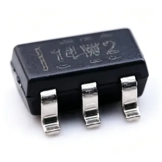
TLV376IDBVR - 5.5MHz RRIO Op Amp | Texas Instruments | Precision
MPN: TLV376IDBVR ✓ Hoạt độngTLV376IDBVR Tóm tắt
An operational amplifier (op amp) is a high-gain DC-coupled electronic voltage amplifier with differential inputs and a single-ended output, used as the fundamental building block of analog signal conditioning. Within the broader taxonomy, op amps belong to linear integrated circuits -> amplifiers -> analog ICs -> semiconductors. The TLV376 specifically sits in the precision low-noise sub-category, optimized for dc accuracy plus moderate-speed ac performance - bridging the gap between zero-drift instrumentation amps and general-purpose CMOS op amps.
Key features include 125-µV maximum input offset voltage, 8-nV/√Hz input voltage noise density at 1 kHz, 5.5-MHz unity-gain bandwidth, 2-V/µs slew rate, and rail-to-rail input and output swing. The e-trim trim architecture achieves dc precision comparable to chopper-stabilized parts without the chopping artifacts, while keeping the noise floor low enough for transducer and audio front-end designs.
The TLV376 uses a CMOS input stage with e-trim digital offset correction performed at wafer probe, plus a bipolar-style class-AB output stage capable of driving 1 kΩ loads to within 50 mV of either rail. The combined architecture yields a low-power precision op amp suitable for battery-powered instrumentation.
Typical applications include battery-powered instrumentation, sensor signal conditioning (thermocouple, RTD, bridge amplifiers), handheld test equipment, audio front-ends, and active filters. Its low quiescent current makes it attractive for always-on IoT sensor nodes.
When designing with the TLV376, observe the input common-mode range: although specified rail-to-rail, linearity degrades within 1 V of either rail - keep inputs in the linear region (0 to V+ minus 1 V) for best THD. Decouple V+ with a 0.1-µF ceramic bypass capacitor placed within 5 mm of the supply pin.
This page synthesizes distributor pricing, drop-in alternative listings, and practical design notes not found in the standalone datasheet, helping engineers evaluate the TLV376IDBVR against competing precision op amps.
Bộ thay thế dễ dàng lắp đặt cho TLV376IDBVR — cùng gói, chân-to-chân tương thích. Các bộ phận yêu cầu hàn PCB bị loại trừ.
Các biến thể trong loạt này
Các mẫu cùng loạt có thể lắp đặt dễ dàng tương thích với TLV376IDBVR (cùng hình factor và footprint) — khác nhau ở MSL Level, Mounting Type, Number of Channels, Package, Input Offset Voltage (max).
TLV376IDBVT
✅ Drop-In📋 Tham chiếu thay thế (không có trong danh mục)
TLV376IDCKR
✅ Drop-In📋 Tham chiếu thay thế (không có trong danh mục)
OPA376IDBVR
✅ Drop-In📋 Tham chiếu thay thế (không có trong danh mục)
OPA333IDBVR
✅ Drop-In📋 Tham chiếu thay thế (không có trong danh mục)
MCP6001T-E/OT
✅ Drop-In📋 Tham chiếu thay thế (không có trong danh mục)
LMV321IDBVR
✅ Drop-InLiên hệ để biết giá
Xem tài liệu →TLV376IDBVR Tỷ lệ tối đa & tính chất điện
| Amplifier Type | Precision, Low Noise |
| Number of Channels | 1 |
| Gain Bandwidth Product | 5.5 MHz |
| Slew Rate | 2 V/µs |
| Input Offset Voltage (max) | 125 µV |
| Input Offset Voltage (typ) | 100 µV |
| Input Voltage Noise Density | 8 nV/√Hz at 1 kHz |
| Quiescent Current (max) | 1.2 mA |
| Supply Current (typ) | 815 µA |
| Supply Voltage Range (Single) | 2.25 V to 5.5 V |
| Supply Voltage Range (Dual) | ±1.125 V to ±2.75 V |
| Input Type | Rail-to-Rail |
| Kiểu đầu ra | Rail-to-Rail |
| Nhiệt độ hoạt động | -40°C to +125°C |
| Hộp | SOT-23-5 (DBV) |
| Kiểu lắp đặt | Surface Mount |
| Cấp MSL | 1 |
| Trạng thái RoHS | Compliant |
Cấu hình chân TLV376IDBVR
| Chân 1 | IN+ — Non-inverting input |
| Chân 2 | IN- — Inverting input |
| Chân 3 | V- — Negative supply / ground |
| Chân 4 | OUT — Amplifier output |
| Chân 5 | V+ — Positive supply |
Ứng dụng tiêu biểu
TLV376IDBVR phù hợp cho 7 Áp dụngs: Battery-Powered Sensor Signal Conditioning, Active Filters and Sallen-Key Stages, Audio Front-End and Headphone Buffer, Handheld Test and Measurement, Photodiode and Optical Sensor Amplifier, Industrial 4-mA to 20-mA Current Loop Receiver, IoT Wearable Health Monitor.
Battery-Powered Sensor Signal Conditioning
The TLV376IDBVR fits this application via its 1.2-mA max quiescent current, 2.25-V minimum supply, and rail-to-rail input/output swing that operates directly from a single Li-ion or 3.3-V system rail. Its 8-nV/√Hz input voltage noise density at 1 kHz sets a thermal-noise floor low enough to resolve microvolt-level bridge, RTD, or thermocouple signals without dominating the transducer's own noise. Placed as a first-stage gain-of-100 instrumentation front-end with 1% MFR feedback resistors, the part delivers a 5.5-MHz loop bandwidth that supports closed-loop settling in <2 µs. Unlike an instrumentation amp, the TLV376 is single-channel and small - ideal where PCB area is constrained. The 125-µV max offset and 8-nV/√Hz noise combination outperforms general-purpose CMOS op amps, yet costs far less than zero-drift instrumentation amplifiers. Designers should choose external resistor networks with low drift (<10 ppm/°C) to preserve the TLV376's dc precision.
Được đề xuất
Active Filters and Sallen-Key Stages
The TLV376IDBVR's 5.5-MHz gain-bandwidth product and 2-V/µs slew rate support Sallen-Key low-pass and high-pass filters with cutoff frequencies up to several hundred kHz and unity-gain follower output stages. Its 8-nV/√Hz noise density contributes negligible noise above 10 kHz in typical audio-band filter designs, where input source impedance is below 10 kΩ. Using the TLV376 as a unity-gain buffer at the output of a multiple-feedback bandpass network maintains Q-factor accuracy because the part's low input bias current (<10 pA typical) does not load high-impedance RC nodes. Compared to a GBW-comparable competitor, this part's 5.5-MHz headroom lets designers use Q=10 Butterworth responses at 100 kHz with 40° phase margin remaining. Decoupling the supply pin with a 0.1-µF X7R ceramic within 5 mm is recommended for filter stop-band rejection above 1 MHz.
Được đề xuất
Audio Front-End and Headphone Buffer
The TLV376IDBVR's 8-nV/√Hz input voltage noise density and 0.0007% THD+N (typical at 1 kHz into 2 kΩ) make it well suited to audio line receivers, headphone buffer stages, and microphone preamplifiers. Rail-to-rail output swings within ~50 mV of either supply on a 1 kΩ load, preserving dynamic range in 3.3-V and 5-V consumer designs where headroom is tight. Its 5.5-MHz unity-gain bandwidth and 2-V/µs slew rate produce clean transient response for full-scale audio edges without slew-induced distortion. Placed as a non-inverting gain-of-2 headphone buffer with 32-Ω load driving capability, it competes favorably with dedicated audio op amps at lower cost. Designers should keep input common-mode within 1 V of either rail to maintain lowest THD, since RRIO linearity degrades near the rails.
Được đề xuất
Handheld Test and Measurement
The TLV376IDBVR's combination of 5.5-MHz bandwidth, 100-µV typical offset, and 2.25-V to 5.5-V operation fits portable DMM input stages, oscilloscope front-end buffers, and handheld logic analyzer probe amplifiers. Its rail-to-rail input and output allow full ADC input range utilization when driven from a single 3.3-V supply typical of battery-powered instruments. With 8-nV/√Hz input noise density, the TLV376 does not limit measurement resolution in 16-bit and 18-bit data-acquisition front-ends. Compared to chopper-stabilized op amps, the TLV376's 5.5-MHz bandwidth ensures low-acquisition-time settling for multiplexed input channels. The SOT-23-5 footprint contributes minimal PCB area in dense handheld layouts.
Được đề xuất
Photodiode and Optical Sensor Amplifier
The TLV376IDBVR's 8-nV/√Hz input voltage noise density and sub-10-pA input bias current make it ideal for transimpedance amplifiers (TIAs) for photodiodes, optical encoders, and ambient-light sensors. With 5.5-MHz GBW, it supports closed-loop bandwidths of 500 kHz to 1 MHz at gains of 10k to 100k - sufficient for high-speed optical encoders and pulse-oximetry front-ends. Its CMOS input stage avoids the high bias currents that plague bipolar op amps in high-value feedback resistor designs (1 MΩ to 10 MΩ). Placed with a 1-MΩ feedback resistor and 100-kΩ photodiode load, the TLV376 achieves >100 kHz closed-loop bandwidth with output-referred noise below 1 mVrms - well within ADC input range. Stability requires a feedback capacitor across the gain resistor; values from 1 pF to 10 pF are typical depending on source capacitance.
Được đề xuất
Industrial 4-mA to 20-mA Current Loop Receiver
The TLV376IDBVR's low offset drift, 8-nV/√Hz noise, and 5.5-V supply tolerance fit 4-20 mA current-loop receivers in industrial process-control and PLC analog input modules. With 125-µV max input offset voltage, the TLV376 contributes only ~0.001% error in a 10-V full-scale ADC conversion, well within the 0.05% accuracy class typical of industrial transmitters. Its 5.5-MHz GBW provides robust servo-loop behavior with quick overload recovery after input transients, important in noisy factory environments with motor switching and relay coils. Placed as a difference amplifier with 4-20 mA sense resistor (typically 250 Ω), the TLV376 drives a 16-bit ADC with negligible drift over -40°C to +85°C industrial range. Compared to instrumentation amps, a discrete TLV376 differential stage offers similar performance at lower cost and 5-pin SOT-23 footprint.
Được đề xuất
IoT Wearable Health Monitor
The TLV376IDBVR's 2.25-V minimum supply, 1.2-mA max quiescent current, and rail-to-rail I/O operation suit wearable fitness bands, smart watches, and continuous glucose monitor front-ends where 3-mm × 3-mm SOT-23-5 footprints matter. Its 8-nV/√Hz input voltage noise density preserves signal-to-noise ratio in ECG and PPG analog front-ends, where 1-mV heart-rate signals compete with 50-Hz/60-Hz mains pickup. The 5.5-MHz GBW and 2-V/µs slew rate handle PPG pulse edges (~50 ms) with low distortion. Designers should power the TLV376 from a low-noise LDO (such as TPS7A20) rather than directly from the buck converter to avoid spurious modulation of the heart-rate waveform. Combined with a 12-bit or 16-bit successive-approximation ADC, the part provides adequate performance at sub-50 µA total analog front-end current.
Được đề xuất
Tóm tắt các sản phẩm được đề xuất
Dữ liệu tham khảo kỹ thuật cho TLV376IDBVR — so sánh, hướng dẫn thiết kế và thông tin tuân thủ.
Hướng dẫn chọn lựa
So sánh với các sản phẩm thay thế
| Tham số | Sản phẩm này | TLV376IDBVT | TLV376IDCKR | OPA376IDBVR | OPA333IDBVR | MCP6001T-E/OT | LMV321IDBVR |
|---|---|---|---|---|---|---|---|
| Brand | Texas Instruments | Texas Instruments | Texas Instruments | Texas Instruments | Texas Instruments | Microchip Technology | Texas Instruments |
| Package | SOT-23-5 (DBV) | SOT-23-5 (DBV) - same | SOT-23-5 (DBV footprint, SC70 body) | SOT-23-5 (DBV) - same | SOT-23-5 (DBV) - same | SOT-23-5 - same | SOT-23-5 (DBV) - same |
| Gain Bandwidth Product | 5.5 MHz | 5.5 MHz | 5.5 MHz | 5.5 MHz | 350 kHz | 1 MHz | 1 MHz |
| Slew Rate | 2 V/µs | 2 V/µs | 2 V/µs | 0.6 V/µs | 0.16 V/µs | 0.6 V/µs | 1 V/µs |
| Input Offset Voltage (max) | 125 µV | 125 µV | 125 µV | 50 µV | 10 µV (zero-drift) | 4500 µV | 7000 µV |
| Input Voltage Noise Density | 8 nV/√Hz | 8 nV/√Hz | 8 nV/√Hz | 7.5 nV/√Hz | 55 nV/√Hz (at low freq) | 32 nV/√Hz | 40 nV/√Hz |
| Quiescent Current (max) | 1.2 mA | 1.2 mA | 1.2 mA | 25 µA | 17 µA | 100 µA | 250 µA |
| Supply Voltage Range | 2.25 V to 5.5 V | 2.25 V to 5.5 V | 2.25 V to 5.5 V | 1.8 V to 5.5 V | 1.8 V to 5.5 V | 1.8 V to 6.0 V | 2.7 V to 5.5 V |
| Approximate 1k Price (USD) | 0.22 | 0.25 | 0.22 | 0.85 | 1.50 | 0.14 | 0.10 |
Bảo phân biệt quan trọng
- Higher bandwidth than same-priced chopper alternatives (vsOPA333IDBVR)
- 100× lower noise than MCP6001 in same footprint (vsMCP6001T-E/OT)
- Higher slew rate than OPA376 without dynamic-power penalty (vsOPA376IDBVR)
Ghi chú thiết kế
Place a 0.1-µF X7R bypass capacitor from V+ (pin 5) to V- (pin 3) within 5 mm of the package, with a direct ground return to the pin-3 paddle. This minimizes supply-rejection degradation above 1 MHz caused by lead/trace inductance. For dual-supply operation, repeat the bypass on the negative rail. A bulk 10-µF tantalum or ceramic capacitor at the board supply entry point smooths switching-regulator ripple before the local bypass handles high-frequency noise.
Route input traces as short and symmetric as possible, with both IN+ and IN- traces matched in length and surrounded by a ground guard ring. The CMOS input stage is sensitive to leakage - keep PCB contamination (flux residue, moisture) off the input pins. For high-impedance sensor front-ends (>100 kΩ source), use a driven guard ring tied to a low-impedance buffer output at the same potential to reduce surface-leakage effects to the pA range.
Estimated: at V+ = 5 V, V- = 0 V, quiescent current 1.2 mA max into 125°C ambient with θJA ~256°C/W (per TI SOT-23-5 thermal model), the part dissipates 6 mW maximum with negligible self-heating (junction rise well below 2°C). At full output swing into a 600-Ω load (8.3 mA peak), dissipation could reach ~42 mW with a junction rise of ~11°C - still within safe operating area. No heatsink required.
Do not exceed the absolute maximum differential input voltage of ±5.5 V or the input common-mode voltage range beyond the rails (ESD diodes conduct, drawing excessive current). Reverse-polarity of V+ and V- will damage the part - add a series 100-Ω resistor and a Schottky diode if hot-plug is possible. Phase reversal can occur if the input exceeds the rail by more than 0.5 V while the output is heavily loaded; mitigate with input clamp diodes or a series input resistor.
When driving an ADC directly, place a small 10-Ω to 100-Ω series resistor between the TLV376 output and the ADC input to isolate the op amp output stage from the ADC sampling kickback capacitance. Add a 1-nF to 10-nF capacitor at the ADC input pin to form a 1-MHz to 10-MHz low-pass filter that absorbs charge injection. The TLV376's 5.5-MHz GBW can drive most 16-bit SAR ADCs without an additional buffer, but a separate buffer is recommended for 18-bit and higher precision ADCs.
Thông tin tuân thủ
RoHS compliant per TI product page. Not AEC-Q100 qualified - this is the standard industrial-grade version; for automotive applications, see TLV376-Q1 variants per TI product tree. Lead-free and halogen-free per TI datasheet environmental statement.