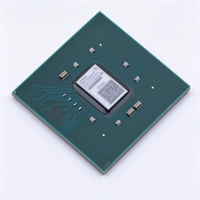
XC7K70T-3FBG484E
XC7K70T-3FBG484E - 65.6K Kintex-7 FPGA | AMD Xilinx
AMD Xilinx XC7K70T-3FBG484E is a Kintex-7 field-programmable gate array with 65,600 logic cells, 285 user I/O, a -3 performance grade, and an FBG484 flip-chip BGA package. The device belongs to the Kintex-7 FPGA family, combining programmable logic, block RAM, DSP resources, programmable I/O, and high-speed connectivity in a single 484-pin package.
A field-programmable gate array is a semiconductor whose digital functions are configured after manufacture through a programmable logic array. Within the FPGA hierarchy, the Kintex-7 family provides a balance of logic density, signal-processing capability, I/O availability, and performance for communications, industrial, instrumentation, aerospace, and defense systems. An FPGA can accelerate parallel algorithms, implement protocol bridges, perform real-time signal processing, and combine multiple fixed-function functions on one board.
The XC7K70T-3FBG484E provides 65,600 logic cells organized as 10,250 adaptive logic modules and includes 4.75 Mbit of embedded memory. Its 285 I/O expand the connection to external memory, transceivers, clocks, data converters, and interface devices. The Kintex-7 family is manufactured on a 28 nm process and uses a 1 V core supply, supporting high-density programmable systems while maintaining a broad ecosystem of design tools, intellectual property, and development hardware.
The -3 suffix identifies the device performance grade, while FBG484 identifies the 484-pin FBG package. The E suffix denotes the extended-temperature product configuration used in industrial and extended operating environments. These suffixes affect qualification, speed, temperature, and ordering rather than the basic Kintex-7 architecture. Package ball assignments, configuration requirements, power sequencing, and design constraints must be checked against the package pinout files and device documentation before a board is released.
Typical applications include industrial Ethernet and network equipment, high-speed test and measurement systems, radar and signal-processing equipment, scientific instrumentation, embedded control, video infrastructure, and communications infrastructure. The 285-I/O package is particularly useful where the design requires numerous parallel digital connections in addition to high-speed serial links, while the 4.75 Mbit of embedded memory supports buffering, packet storage, and data-retention functions.
The primary design consideration is package complexity. A 484-ball BGA demands careful PCB escape routing, power-plane design, decoupling, thermal planning, and assembly-process control. Use the package-specific ball map and recommended power architecture rather than inferring connectivity from another FPGA package. Verify signal integrity on every high-speed interface and preserve the specified configuration and power-supply sequencing behavior.
This product analysis consolidates the device identity, package details, capacity data, source links, drop-in family alternatives, and practical design considerations into one engineering-focused reference. It is intended to help designers assess whether the XC7K70T-3FBG484E provides the required Kintex-7 resources before beginning schematic capture, PCB layout, and Vivado implementation.
詢價
聯絡我們