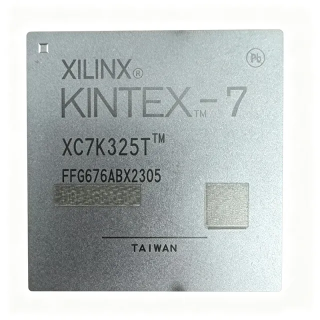
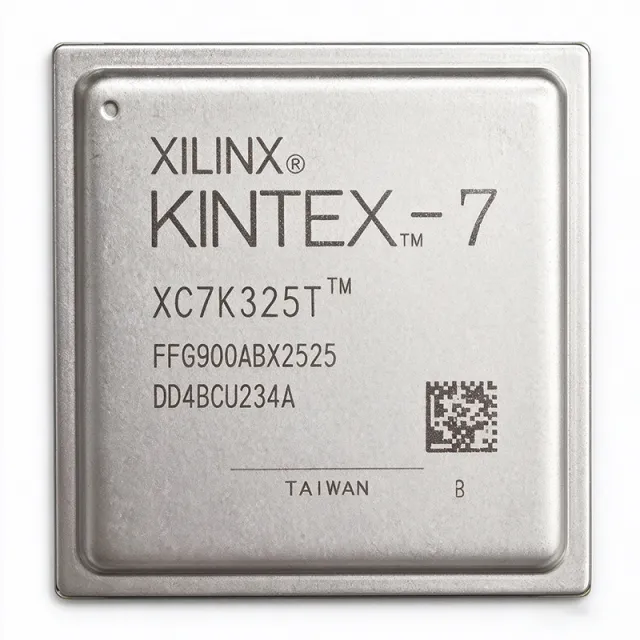
XC7K325T-2FBG900C
XC7K325T-2FBG900C - 326K-Cell Kintex-7 FPGA | AMD
The AMD XC7K325T-2FBG900C is a Kintex-7 field-programmable gate array with 326,080 logic cells, 16,020 Kb of block RAM, 840 DSP slices, and 500 I/O sites in a 900-pin lidless FCBGA package. It is manufactured on 28 nm technology, operates from a 1 V core supply, and combines the -2 performance grade with commercial junction-temperature coverage from 0°C to 85°C.
A field-programmable gate array is a programmable digital semiconductor used to implement logic, control, signal processing, connectivity, and embedded systems. The Kintex-7 family occupies the middle ground between low-cost Spartan-7 devices and high-end Virtex devices, balancing logic density, DSP resources, memory bandwidth, and general-purpose I/O. Within the FPGA hierarchy, this device provides substantially more parallel processing capacity than smaller FPGAs while remaining suitable for communications, industrial control, test equipment, and embedded video systems.
The principal resources are 326,080 configurable logic cells, 16,020 Kb of block RAM, 840 DSP slices, and 500 I/O sites. These resources support parallel data pipelines, digital filtering, control logic, protocol handling, and high-speed external interfaces. The -2 ordering code identifies the device performance grade, while the FBG900 suffix identifies the 900-ball package and its exact footprint. The C suffix denotes the commercial temperature option used in the target ordering code.
At the architecture level, the 28 nm Kintex-7 device combines programmable logic with dedicated arithmetic and block-memory resources. DSP slices accelerate multiply-accumulate operations commonly used in filters, transforms, modulation, and signal conditioning. Block RAM provides on-chip storage for buffers, lookup tables, packet data, and wide datapaths. Configurable I/O support allows the FPGA to connect to external memory, transceivers, converters, clocks, and board-level control signals.
Typical uses include industrial automation, communications infrastructure, instrumentation, high-speed test and measurement, embedded processing, video and image pipelines, and digital signal processing. The large FBG900 footprint provides access to many I/O and power connections, but it also demands careful PCB layout, multilayer routing, thermal design, and package-aware assembly planning.
The principal engineering consideration is that a drop-in replacement must reproduce the FBG900 footprint, ball assignment, voltage requirements, configuration behavior, and device resources. Speed-grade or temperature-grade substitutions may preserve the same PCB land pattern but can change timing guarantees and environmental margins. Use AMD pinout files, UG475, and the Kintex-7 data sheet to validate every migration before production release.
This page combines device specifications, same-package replacement options, interface considerations, and design guidance to help engineers evaluate the XC7K325T-2FBG900C beyond a basic catalog listing. It is intended for engineers who need a precise technical assessment of density, packaging, thermal grade, and replacement risk.
詢價
聯絡我們