EPC2LC20 vs EPC1LI20 比較
詳細並排比較 EPC2LC20 由 Altera 與 EPC1LI20 由 Altera. 比較關鍵規格、電氣參數、封裝、生命週期狀態、價格與供貨情況,以找出最符合您設計需求的元件。
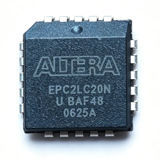

規格比較
| 參數 | EPC2LC20 | EPC1LI20 |
|---|---|---|
| 品牌 | Altera | Altera |
| 類別 | Memory ICs | Memory ICs |
| 生命週期狀態 | NRND | Obsolete |
| 記憶體類型 | Non-volatile configuration PROM | OTP Configuration PROM (EPROM-based) |
| 記憶體容量 | 1.6 Mbit | 1 Mb (1,048,576 bits) |
| Configuration Interface | Serial (x1) to FPGA via DCLK/nCONFIG/nSTATUS/CONF_DONE | Altera Passive Serial / Altera Active Serial / JTAG (IEEE 1149.1) |
| Programming Interface | IEEE 1149.1 (JTAG) ISP, 5.0-V and 3.3-V tolerant | — |
| Supply Voltage VCC | 3.0 V to 3.6 V (3.3-V operation) | — |
| ISP Voltage Range | 5.0 V or 3.3 V | — |
| Supported FPGA Families | ACEX 1K, APEX 20K/20KC/20KE, APEX II, Arria GX, Cyclone, Cyclone II, FLEX 10K, FLEX 6000, MAX 9000 | — |
| Cascade Support | Yes - daisy-chain multiple EPC2 devices via JTAG for larger bitstreams | — |
| 封裝 | 20-pin PLCC (J-lead, 9x9 mm) | 20-pin PLCC (J-lead, 9x9 mm) |
| 安裝類型 | Surface Mount | Surface Mount (PLCC socket compatible) |
| 工作溫度 | -40C to +85C (industrial) [DATA_NEEDED: exact grade from datasheet] | [DATA_NEEDED: operating temperature range] |
| RoHS 狀態 | Non-Compliant (original Altera Pb-containing part) | [DATA_NEEDED: RoHS status - original Altera part may be non-RoHS SnPb finish] |
| Lead-Free Version | EPC2LC20N available as lead-free equivalent | — |
| Programming Support | Altera Programming Unit (APU), Quartus II, JTAG programmer | — |
| Boundary-Scan | IEEE 1149.1 compliant, 8-bit or 16-bit JTAG | — |
| Maximum Configuration Clock | — | 8 MHz |
| Supply Voltage (VCC) | — | 5.0 V (4.75 V to 5.25 V) |
| Programming Voltage (VPP) | — | 12.75 V (typical, factory-programmed via JTAG) |
| 腳位數 | — | 20 |
| Cascading Support | — | Yes (nCASC pin for multi-device daisy chain) |
| Endurance | — | OTP (one-time programmable, 1000 erase-equivalent UV cycles for pre-program erase) |
| JTAG Programming | — | Yes (in-system via IEEE 1149.1) |
| Compatible FPGA Families | — | FLEX 8000, FLEX 10K, ACEX 1K, APEX 20K, Mercury |
| MSL 等級 | — | 1 (per Partstack datasheet record) |