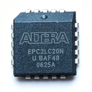
EPC1LI20 - 1Mb OTP FPGA Config PROM 20-PLCC | Altera / Intel
MPN: EPC1LI20 ✗ 停產EPC1LI20 概覽
A configuration PROM is a non-volatile memory IC whose sole purpose is to hold the bitstream for an SRAM-based FPGA. Because SRAM FPGAs lose their configuration when power is removed, a configuration device such as the EPC1LI20 is required in every standalone board design. The EPC1 family belongs to the broader category of FPGA configuration memory (FPGA > Configuration Memory > Configuration PROM > Non-volatile Memory > Memory IC), and is typically selected over parallel PROMs or microcontrollers because it provides a purpose-built FPGA configuration interface, eliminating firmware development and reducing board area.
Key features of the EPC1LI20 include 1 Mb of OTP storage, a serial configuration clock of up to 8 MHz (per Altera datasheet Table 1), simple four-wire interface (nCS, DCLK, DATA, OE), 5.0 V single-supply operation, low-power CMOS process, and a 1000-erase-equivalent PROM endurance rating. Programming is performed in-system through the standard JTAG (IEEE 1149.1) chain, allowing board-level programming without removing the device. The 20-pin PLCC package offers socket compatibility for prototyping and field-replacement scenarios.
Architecturally, the EPC1LI20 contains an oscillator, address counter, programming voltage generator, and a UV-erasable EPROM-style memory array. The internal state machine sequences through the array on each rising DCLK edge, presenting the next data byte on the DATA output. An optional cascading mode allows multiple EPC1 devices to be daisy-chained to configure large FPGAs (e.g., APEX 20K) or multi-FPGAs systems, using the nCASC pin for handshaking.
Typical applications include single-FPGA standalone configuration, multi-FPGA board configuration with daisy-chained PROMs, FPGA development platforms, factory programming stations, industrial control and factory automation boards, and military/aerospace SRAM-FPGA systems requiring legacy 5V logic compatibility. Designers choose EPC1LI20 over flash-based EPC2 when the bitstream is finalized and cost-effective OTP storage is preferred.
When designing with the EPC1LI20, ensure that the FPGA's configuration mode pins MSEL[1:0] are correctly set for the Altera serial configuration scheme. Decoupling: place a 0.1 uF ceramic capacitor close to VCC and another close to the VPP pin. The JTAG chain should include proper TMS/TCK pull-ups as recommended in IEEE 1149.1 boundary-scan practice. For multi-device cascading, verify timing against the FPGA's CONF_DONE and nSTATUS handshakes.
This page synthesizes distributor pricing, cross-reference data from FindChips, and practical JTAG-programming notes not found in a single Altera datasheet, giving engineers a complete view of the EPC1LI20 lifecycle, drop-in alternatives, and design trade-offs.
直接替換替代品,適用於 EPC1LI20 — 相同封裝,腳位對腳位相容。需重新設計 PCB 的不同封裝零件不列入。
此系列的變體
與下列產品可直接替換的同系列型號: EPC1LI20 (相同外形與佔位) — 差異在於 Memory Type, Mounting Type, Package, Memory Size, Configuration Interface.
EPC1LC20
✅ 直接替換聯絡詢價
查看資料表 →EPC2LI20
✅ 直接替換聯絡詢價
查看資料表 →EPC2LC20
✅ 直接替換✗ 缺貨
$7.2 / 單位
查看資料表 →EPC1LC20N
✅ 直接替換聯絡詢價
查看資料表 →EPC1441LC20
✅ 直接替換聯絡詢價
查看資料表 →EPC1LI20 最大額定值與電氣特性
| 記憶體類型 | OTP Configuration PROM (EPROM-based) |
| 記憶體容量 | 1 Mb (1,048,576 bits) |
| Configuration Interface | Altera Passive Serial / Altera Active Serial / JTAG (IEEE 1149.1) |
| Maximum Configuration Clock | 8 MHz |
| Supply Voltage (VCC) | 5.0 V (4.75 V to 5.25 V) |
| Programming Voltage (VPP) | 12.75 V (typical, factory-programmed via JTAG) |
| 封裝 | 20-pin PLCC (J-lead, 9x9 mm) |
| 腳位數 | 20 |
| Cascading Support | Yes (nCASC pin for multi-device daisy chain) |
| Endurance | OTP (one-time programmable, 1000 erase-equivalent UV cycles for pre-program erase) |
| JTAG Programming | Yes (in-system via IEEE 1149.1) |
| Compatible FPGA Families | FLEX 8000, FLEX 10K, ACEX 1K, APEX 20K, Mercury |
| 安裝類型 | Surface Mount (PLCC socket compatible) |
| MSL 等級 | 1 (per Partstack datasheet record) |
EPC1LI20 腳位配置
| 腳位 1 | VCC — 5.0 V supply voltage |
| 腳位 2 | DATA — Serial data output to FPGA |
| 腳位 3 | DCLK — Configuration clock input |
| 腳位 4 | OE — Output enable (active low) from FPGA nSTATUS |
| 腳位 5 | nCS — Chip select (active low) |
| 腳位 6 | nCASC — Cascade output to next EPC device |
| 腳位 7 | nINIT_CONF — Initiate configuration (active low) |
| 腳位 8 | GND — Ground |
| 腳位 9 | TDI — JTAG Test Data In |
| 腳位 10 | TDO — JTAG Test Data Out |
| 腳位 11 | TMS — JTAG Test Mode Select |
| 腳位 12 | TCK — JTAG Test Clock |
| 腳位 13 | NC — Not connected (per datasheet) |
| 腳位 14 | NC — Not connected (per datasheet) |
| 腳位 15 | VPP — Programming voltage (factory only) |
| 腳位 16 | NC — Not connected (per datasheet) |
| 腳位 17 | NC — Not connected (per datasheet) |
| 腳位 18 | NC — Not connected (per datasheet) |
| 腳位 19 | NC — Not connected (per datasheet) |
| 腳位 20 | VCC — 5.0 V supply (redundant to pin 1) |
典型應用
EPC1LI20 適用於 6 應用s: Standalone Altera FLEX 10K FPGA Configuration, APEX 20K Multi-FPGA Configuration with Cascaded PROMs, Industrial Control Board FPGA Boot Source, Legacy 5 V Avionics & Military Board Repair, FPGA Development Platform Configuration, Telecom Line Card FPGA Configuration.
Standalone Altera FLEX 10K FPGA Configuration
The EPC1LI20 is the canonical 5.0 V configuration memory for the Altera FLEX 10K family. With 1 Mb of OTP storage and an 8 MHz maximum DCLK, it loads the FLEX 10K bitstream in roughly 130 ms from a single 5 V rail. Designers wire nCS to the FPGA's nCONFIG, DCLK to the FPGA's DCLK, and DATA to DATA0; CONF_DONE pulls high when the FPGA has finished loading. The 20-PLCC package is socket-compatible for in-the-field re-programming via JTAG using a USB-Blaster.
推薦
APEX 20K Multi-FPGA Configuration with Cascaded PROMs
The APEX 20K family needs more than 1 Mb of bitstream for the larger devices, so designers daisy-chain multiple EPC1LI20 PROMs using the nCASC pin to stream a contiguous configuration image. The first device's nCASC drives the nCS of the second, and CONF_DONE is asserted only after the last device in the chain has finished streaming. This makes the EPC1LI20 well suited to factory automation, telecom, and military boards that pair APEX 20K with multiple legacy 5 V peripherals.
推薦
Industrial Control Board FPGA Boot Source
In 24V industrial PLC and motor-control boards, the EPC1LI20 provides a 5.0 V non-volatile boot source for ACEX 1K and FLEX 10K FPGAs that handle deterministic logic and DSP. The OTP nature of the EPC1LI20 protects the bitstream from accidental field re-flash, which is a regulatory and safety benefit in factory automation. The 20-PLCC socket allows the OEM to pre-program the configuration PROM in a fixture, then place it on the production board to lock the firmware at build time.
推薦
Legacy 5 V Avionics & Military Board Repair
Many military and avionics boards designed in the late 1990s and early 2000s use Altera FLEX 8000 and ACEX 1K FPGAs paired with EPC1LI20 PROMs. Because the part is obsolete but form-fit-function equivalent to EPC1LC20N and EPC1LC20 lead-free variants, the EPC1LI20 remains in the bill of materials for MRO and field-repair activities. The 20-PLCC socket allows depot-level replacement without reworking the PCB, and the 5 V-only logic matches legacy 54LS/54ACT interface chips still in service.
推薦
FPGA Development Platform Configuration
University labs and FPGA development kits still ship the EPC1LI20 in PLCC sockets to support FLEX 10K and APEX 20K evaluation boards. The OTP PROM paired with the Altera Quartus Programmer (ByteBlasterMV/USB-Blaster JTAG chain) gives students a hands-on view of FPGA configuration timing, CONF_DONE handshaking, and JTAG boundary-scan. The 20-PLCC form factor is large enough to probe with an oscilloscope, which is valuable for teaching configuration clock behavior at 8 MHz.
推薦
Telecom Line Card FPGA Configuration
Telecom line cards designed in the 2000s use FLEX 10K or APEX 20K FPGAs for framer and protocol logic, configured by an EPC1LI20 to provide fast 5 V power-up boot. The 1 Mb density covers the typical bitstream for a single-channel framer. Because telecom-grade boards are kept in service for 15-20 years, the EPC1LI20 (and its lead-free twin EPC1LC20N) remain in long-term storage at contract manufacturers, and the 20-PLCC socket simplifies board-level swap during depot repair.
推薦
推薦產品摘要
工程參考資料,適用於 EPC1LI20 — 比較、設計指引及合規資訊。
選型指南
與替代品比較
| 參數 | 本產品 | EPC1LC20 | EPC1LC20N | EPC2LI20 | EPC2LC20 | EPC1441LC20 |
|---|---|---|---|---|---|---|
| Package | 20-PLCC (9x9 mm) | 20-PLCC (same) | 20-PLCC (same) | 20-PLCC (same) | 20-PLCC (same) | 20-PLCC (same) |
| Brand | Altera / Intel | Altera / Intel | Altera / Intel | Altera / Intel | Altera / Intel | Altera / Intel |
| Memory Size | 1 Mb | 1 Mb | 1 Mb | 1.6 Mb | 1.6 Mb | 144 Kb |
| Memory Type | OTP EPROM | OTP EPROM | OTP EPROM | Flash (reprogrammable) | Flash (reprogrammable) | OTP EPROM |
| Max DCLK | 8 MHz | 8 MHz | 8 MHz | 8 MHz (configurable higher) | 8 MHz (configurable higher) | 8 MHz |
| Supply Voltage | 5.0 V | 5.0 V | 5.0 V | 3.3 V or 5.0 V | 3.3 V or 5.0 V | 5.0 V |
| Reprogrammable | No (OTP) | No (OTP) | No (OTP) | Yes (flash, 100+ cycles) | Yes (flash, 100+ cycles) | No (OTP) |
| Lifecycle | Obsolete | Last-time-buy | Last-time-buy | Last-time-buy (active replacement recommended) | Last-time-buy | Last-time-buy |
| Unit Price (qty 100, USD) | 11.20 | 10.50 | 10.80 | 12.50 | 12.80 | 9.50 |
主要差異化特點
- Same 20-PLCC footprint with lead-free and flash variants available (對比EPC1LC20N (Altera lead-free twin))
- Reprogrammable flash option in same 20-PLCC footprint (對比EPC2LI20 (Altera flash replacement))
- Smaller-density 144 Kb variant for compact bitstreams (對比EPC1441LC20 (Altera low-density OTP))
設計說明
The EPC1LI20 requires a stable 5.0 V supply (4.75 V to 5.25 V) on pin 1 and pin 20, plus a clean GND on pin 8. Place a 0.1 uF decoupling capacitor within 5 mm of VCC and a 10 uF bulk capacitor on the same 5 V rail. The programming voltage (VPP, pin 15) is internally generated and only needs a 0.1 uF local decoupling cap. Avoid switching the 5 V rail with high di/dt loads during the first 200 ms of configuration, since DCLK distortion can corrupt the bitstream.
The 20-pin PLCC footprint is the standard JEDEC MO-047 land pattern. Use a PLCC socket (e.g., 3M Textool) for prototyping so the device can be UV-erased and replaced. Keep the JTAG chain traces (TCK, TMS, TDI, TDO) short and matched, with 10 kohm pull-ups on TMS and TCK as recommended by IEEE 1149.1 boundary-scan practice. The DATA and DCLK traces to the FPGA should be length-matched within 25 mm to avoid configuration skew on multi-board systems.
Do not use the EPC1LI20 with a 3.3 V-only FPGA VCCO bank - the EPC1 outputs 5.0 V CMOS levels and will over-drive 3.3 V I/O. For 3.3 V FPGAs, migrate to the EPC2LI20 (3.3V/5V dual) or use a level-shifter. Do not assume JTAG-programmed PROMs can be re-erased: the EPC1 is OTP via JTAG; only UV exposure through the quartz window can clear it. Also, do not cascade the EPC1LI20 with the EPC2 family without checking the cascade timing - they use different nCASC handshaking.
合規資訊
Original Altera EPC1LI20 ships with SnPb (leaded) finish per Partstack Terminal Finish record; RoHS and REACH status not confirmed in web data. Use EPC1LC20N for RoHS-compliant assemblies.