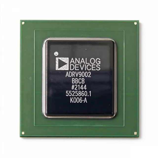
ADRV9002BBCZ-REEL - Dual RF Transceiver 30MHz-6GHz | Analog Devices
MPN: ADRV9002BBCZ-REEL ✓ 啟用中| 數量 | 單價 | 小計 |
|---|---|---|
| 1 | $1012.5 | $1,012.50 |
| 10 | $731.25 | $7,312.50 |
| 100 | $646.875 | $64,687.50 |
| 500 | $618.75 | $309,375.00 |
| 1,000 | $590.625 | $590,625.00 |
ADRV9002BBCZ-REEL 概覽
An RF transceiver is a device that combines both a transmitter and a receiver in a single package, sharing common circuitry. The ADRV9002 is a system-on-chip (SoC) that integrates the RF front-end, analog-to-digital converters (ADCs), digital-to-analog converters (DACs), and digital signal processing (DSP) blocks. This level of integration reduces component count, board space, and design complexity, making it ideal for software-defined radios (SDR) and other advanced wireless systems.
Key features of the ADRV9002 include dual-channel operation, a wide frequency range of 30 MHz to 6 GHz, and support for both narrow-band and wideband signals. The device offers high linearity and dynamic range, ensuring reliable performance in demanding environments. It also includes integrated synthesizers, reducing the need for external PLLs and VCOs. The power output is 7.8 dBm, and the device operates from a single 3.3V supply.
The ADRV9002 uses advanced CMOS technology to achieve high performance with low power consumption. The digital signal processing functions include filtering, gain control, and calibration, which are configurable via a serial peripheral interface (SPI). The device supports multiple operating modes, including TDD and FDD, and can be programmed for various bandwidths and sample rates. The integrated synthesizers provide low phase noise, essential for high-quality signal transmission and reception.
Typical applications for the ADRV9002 include 5G NR base stations, small cells, macro cells, and other wireless infrastructure. It is also used in military and aerospace communications, radar systems, and test and measurement equipment. The wide frequency range and dual-channel capability make it a versatile choice for many RF designs.
When designing with the ADRV9002, careful attention must be paid to power supply decoupling and thermal management. The device requires a clean 3.3V supply and adequate grounding to achieve optimal performance. The exposed pad on the package should be soldered to a thermal via array to dissipate heat effectively.
直接替換替代品,適用於 ADRV9002BBCZ-REEL — 相同封裝,腳位對腳位相容。需重新設計 PCB 的不同封裝零件不列入。
此系列的變體
與下列產品可直接替換的同系列型號: ADRV9002BBCZ-REEL (相同外形與佔位) — 差異在於 Frequency Range, Package, Interface, Supply Voltage, Type.
快速比較工具 — 選擇替代零件進行並排比較:
ADRV9002BBCZ
聯絡詢價
查看資料表 →ADRV9004BBCZ
聯絡詢價
查看資料表 →AD9371BBCZ
聯絡詢價
查看資料表 →AD9361BBCZ
✗ 缺貨
$62 / 單位
查看資料表 →ADRV9001BBCZ
📋 參考替代品(不在目錄中)
ADRV9002BBCZ-REEL 規格
| Type | TxRx Only |
| Frequency Range | 30 MHz ~ 6 GHz |
| Number of Channels | 2 Tx, 2 Rx |
| Power Output | 7.8 dBm |
| 封裝 | 196-TFBGA, CSPBGA |
| 安裝類型 | Surface Mount |
| 工作溫度 | -40°C to +85°C |
| 供應電壓 | 3.3 V |
| Data Interface | SPI |
| Modulation | Narrow-band and wideband |
| RoHS 狀態 | Compliant |
ADRV9002BBCZ-REEL 腳位配置
| 腳位 A1 | GND — Ground |
| 腳位 A2 | TX1_P — Transmitter 1 positive output |
| 腳位 A3 | TX1_N — Transmitter 1 negative output |
| 腳位 B1 | VDD — Power supply |
| 腳位 B2 | TX2_P — Transmitter 2 positive output |
| 腳位 B3 | TX2_N — Transmitter 2 negative output |
| 腳位 C1 | RX1_P — Receiver 1 positive input |
| 腳位 C2 | RX1_N — Receiver 1 negative input |
| 腳位 C3 | RX2_P — Receiver 2 positive input |
| 腳位 D1 | RX2_N — Receiver 2 negative input |
| 腳位 D2 | SPI_CLK — SPI clock |
| 腳位 D3 | SPI_MOSI — SPI master out slave in |
典型應用
ADRV9002BBCZ-REEL 適用於 6 應用s: 5G NR Base Stations, Software-Defined Radio (SDR), Military and Aerospace Communications, Test and Measurement Equipment, IoT Gateways and Edge Computing, Radar Systems.
5G NR Base Stations
The ADRV9002BBCZ-REEL is ideal for 5G NR base stations due to its wide frequency range (30 MHz to 6 GHz) and dual-channel architecture. It supports MIMO and carrier aggregation, enabling high data rates and reliable connectivity. The integrated synthesizers and DSP functions reduce external component count, simplifying design and lowering BOM cost. Its high linearity and dynamic range ensure excellent signal quality even in dense urban environments, making it a preferred choice for macro cells and small cells.
推薦
Software-Defined Radio (SDR)
The ADRV9002BBCZ-REEL is a perfect fit for SDR platforms because it covers a broad frequency range from 30 MHz to 6 GHz, allowing a single hardware design to support multiple communication standards. Its dual-channel capability enables simultaneous transmit and receive, essential for full-duplex SDR. The integrated DSP functions handle filtering and gain control, reducing the processing load on the FPGA. This makes it a versatile and cost-effective solution for military, amateur, and commercial SDR applications.
推薦
Military and Aerospace Communications
The ADRV9002BBCZ-REEL is well-suited for military and aerospace communications due to its wide frequency coverage and robust performance. It operates from 30 MHz to 6 GHz, covering HF, VHF, UHF, and microwave bands used in tactical radios and satellite communications. The dual-channel architecture supports frequency hopping and diversity reception, enhancing link reliability. Its high dynamic range and linearity ensure clear communication in contested electromagnetic environments, making it a trusted choice for defense applications.
推薦
Test and Measurement Equipment
The ADRV9002BBCZ-REEL is an excellent choice for test and measurement equipment such as spectrum analyzers, signal generators, and channel emulators. Its wide frequency range and dual-channel capability allow simultaneous signal generation and analysis. The integrated synthesizers provide low phase noise, essential for accurate measurements. The device's high linearity and dynamic range ensure precise signal reproduction, making it a valuable component for R&D and production test systems.
推薦
IoT Gateways and Edge Computing
The ADRV9002BBCZ-REEL is suitable for IoT gateways and edge computing devices that require multi-band, multi-standard connectivity. Its wide frequency range supports various IoT protocols such as LoRa, NB-IoT, and Wi-Fi. The dual-channel architecture enables simultaneous operation on different bands, improving network capacity. The integrated DSP functions reduce the need for external processing, lowering power consumption and cost. This makes it an ideal solution for smart city and industrial IoT applications.
推薦
Radar Systems
The ADRV9002BBCZ-REEL is well-suited for radar systems, including automotive radar, weather radar, and surveillance radar. Its wide frequency range and dual-channel capability support FMCW and pulse-Doppler radar architectures. The high linearity and dynamic range ensure accurate target detection and ranging. The integrated synthesizers provide stable frequency generation, essential for coherent radar processing. This makes it a reliable choice for both commercial and defense radar applications.
推薦
推薦產品摘要
工程參考資料,適用於 ADRV9002BBCZ-REEL — 比較、設計指引及合規資訊。
選型指南
與替代品比較
| 參數 | 本產品 | ADRV9002BBCZ | ADRV9004BBCZ | AD9371BBCZ |
|---|---|---|---|---|
| Package | 196-TFBGA, CSPBGA | 196-TFBGA, CSPBGA | 196-TFBGA, CSPBGA | 196-TFBGA, CSPBGA |
| Brand | Analog Devices | Analog Devices | Analog Devices | Analog Devices |
| Frequency Range | 30 MHz ~ 6 GHz | 30 MHz ~ 6 GHz | 30 MHz ~ 6 GHz | 300 MHz ~ 6 GHz |
| Number of Channels | 2 Tx, 2 Rx | 2 Tx, 2 Rx | 4 Tx, 4 Rx | 2 Tx, 2 Rx |
| Supply Voltage | 3.3 V | 3.3 V | 3.3 V | 3.3 V |
| Operating Temperature | -40°C to +85°C | -40°C to +85°C | -40°C to +85°C | -40°C to +85°C |
| RoHS | Compliant | Compliant | Compliant | Compliant |
主要差異化特點
- Wide frequency range from 30 MHz to 6 GHz (對比AD9361BBCZ)
- Dual-channel architecture (對比AD9361BBCZ)
- Integrated DSP functions (對比AD9371BBCZ)
設計說明
The ADRV9002BBCZ-REEL requires a clean 3.3V supply. Use low-dropout regulators (LDOs) with high PSRR to minimize noise. Place decoupling capacitors (100nF and 10uF) close to each power pin. For optimal performance, use a dedicated power plane and avoid sharing with digital circuitry.
The device can dissipate significant power, especially during transmit. Ensure adequate thermal management by soldering the exposed pad to a thermal via array and providing a copper pour on the PCB. The thermal resistance values are specified in the datasheet Table 15, based on JEDEC JESD51-12. For high-power operation, consider adding a heatsink or forced air cooling.
For RF performance, use controlled impedance traces for TX and RX lines. Keep RF traces short and shielded to minimize parasitic inductance and crosstalk. Follow the layout guidelines in the datasheet, including grounding and via placement. Use a 4-layer PCB with dedicated ground and power planes for best results.
合規資訊
RoHS compliant per distributor data. Other compliance info not specified in provided data.