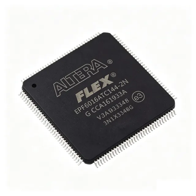
EPF6016ATC144-2 - FLEX 6000 FPGA, 16K Gates, 117 I/O | Intel
MPN: EPF6016ATC144-2 ✓ 啟用中| 數量 | 單價 | 小計 |
|---|---|---|
| 1 | $22.5 | $22.50 |
| 10 | $19.8 | $198.00 |
| 100 | $17.25 | $1,725.00 |
| 500 | $15.1 | $7,550.00 |
| 1,000 | $13.85 | $13,850.00 |
EPF6016ATC144-2 概覽
What is an FPGA? A Field-Programmable Gate Array (FPGA) is a semiconductor IC containing a matrix of configurable logic blocks (CLBs), programmable interconnect, and I/O cells, all defined by a user-supplied bitstream after manufacturing. FPGAs sit between fixed-function ASICs and software-driven processors in the digital-design hierarchy, offering hardware-timed parallelism, fast time-to-prototype, and field re-programmability for design iteration, algorithm acceleration, and glue-logic integration. The FLEX 6000 family targets low-to-mid density glue logic and is part of the broader programmable logic device (PLD) taxonomy.
Key features of the EPF6016ATC144-2 include 117 user I/Os, 132 LABs, on-chip SRAM-based configuration memory, in-system programmability via JTAG (IEEE 1149.1), and support for Altera MAX+PLUS II and Quartus design flows. The device operates from a single supply voltage and supports the commercial temperature grade. Carry chains support high-speed arithmetic functions such as counters and adders, while cascade chains implement wide-input functions with minimum delay. Dedicated clock pins and global routing enable deterministic timing for synchronous designs.
The EPF6010/EPF6016 family uses the OptiFLEX architecture with continuous horizontal routing across rows and vertical routing in columns, balancing density and routability for designs up to ~16K gates. The architecture supports LPM, VHDL, Verilog HDL, and EDIF 2.0/3.0 design entry, allowing seamless integration with third-party EDA synthesis and simulation tools. Internal configuration memory is volatile and must be loaded from an external serial or parallel PROM at power-up, or via JTAG.
Typical applications for the EPF6016ATC144-2 include glue logic for industrial control boards, I/O expansion and bus interfacing, prototyping of mid-density digital designs, replacement of discrete TTL/CMOS logic, custom peripheral controllers in embedded systems, and educational platforms teaching FPGA design with MAX+PLUS II. The 117 I/Os make it suitable for designs with moderate I/O count, while the 144-pin LQFP package simplifies PCB assembly with standard surface-mount equipment.
When designing with this device, consider that configuration memory is volatile - a serial configuration EPROM (e.g., EPC2, EPC4) is required to load the bitstream on power-up, or JTAG can be used for prototype programming. The 144-pin LQFP package has a 0.5 mm pin pitch and requires careful PCB layout for signal integrity. Decoupling capacitors (0.1 µF and 10 µF) should be placed adjacent to every supply pin to minimize switching noise.
This page synthesizes distributor pricing, lifecycle data, drop-in package-compatible alternatives from the FLEX 6000/10K family, and practical design notes not found in the manufacturer datasheet alone, helping engineers select the right pin-compatible FPGA for legacy or new designs.
直接替換替代品,適用於 EPF6016ATC144-2 — 相同封裝,腳位對腳位相容。需重新設計 PCB 的不同封裝零件不列入。
此系列的變體
與下列產品可直接替換的同系列型號: EPF6016ATC144-2 (相同外形與佔位) — 差異在於 Package, Configuration Method, Operating Temperature, Process Technology, Speed Grade.
快速比較工具 — 選擇替代零件進行並排比較:
EPF6016ATC144-1
聯絡詢價
查看資料表 →EPF6016ATC144-1N
聯絡詢價
查看資料表 →EPF6010ATC144-2
聯絡詢價
查看資料表 →EPF6010ATC144-1
聯絡詢價
查看資料表 →EPF6010ATC144-3
聯絡詢價
查看資料表 →EPF6016ATC144-2 最大額定值與電氣特性
| Manufacturer | Intel (formerly Altera) |
| Series | FLEX 6000 |
| Family | OptiFLEX architecture |
| Device Type | FPGA - Field Programmable Gate Array |
| Typical Gates | 16,000 |
| Maximum Logic Elements | 24,000 |
| Logic Elements (LE) | 1,320 |
| Logic Array Blocks (LAB) | 132 (10 LEs each) |
| User I/Os | 117 |
| 封裝 | 144-pin LQFP (LFQFP) |
| 安裝類型 | Surface Mount |
| Process Technology | 0.30 µm CMOS SRAM |
| Configuration Memory | SRAM (volatile) |
| Programming Interface | JTAG (IEEE 1149.1) |
| 工作溫度 | 0 °C to +85 °C (commercial) |
EPF6016ATC144-2 腳位配置
| 腳位 1 | I/O — User I/O pin |
| 腳位 2 | I/O — User I/O pin |
| 腳位 3 | I/O — User I/O pin |
| 腳位 4 | I/O — User I/O pin |
| 腳位 5 | I/O — User I/O pin |
| 腳位 6 | VCC — Supply voltage |
| 腳位 7 | I/O — User I/O pin |
| 腳位 8 | I/O — User I/O pin |
| 腳位 9 | I/O — User I/O pin |
| 腳位 10 | I/O — User I/O pin |
| 腳位 11 | I/O — User I/O pin |
| 腳位 12 | GND — Ground |
| 腳位 13 | I/O — User I/O pin |
| 腳位 14 | I/O — User I/O pin |
| 腳位 15 | I/O — User I/O pin |
| 腳位 16 | I/O — User I/O pin |
| 腳位 17 | I/O — User I/O pin |
| 腳位 18 | I/O — User I/O pin |
| 腳位 19 | I/O — User I/O pin |
| 腳位 20 | I/O — User I/O pin |
| 腳位 21 | I/O — User I/O pin |
| 腳位 22 | VCC — Supply voltage |
| 腳位 23 | I/O — User I/O pin |
| 腳位 24 | I/O — User I/O pin |
| 腳位 25 | I/O — User I/O pin |
| 腳位 26 | I/O — User I/O pin |
| 腳位 27 | I/O — User I/O pin |
| 腳位 28 | GND — Ground |
| 腳位 29 | I/O — User I/O pin |
| 腳位 30 | I/O — User I/O pin |
| 腳位 31 | I/O — User I/O pin |
| 腳位 32 | I/O — User I/O pin |
| 腳位 33 | I/O — User I/O pin |
| 腳位 34 | I/O — User I/O pin |
| 腳位 35 | I/O — User I/O pin |
| 腳位 36 | I/O — User I/O pin |
| 腳位 37 | VCC — Supply voltage |
| 腳位 38 | I/O — User I/O pin |
| 腳位 39 | I/O — User I/O pin |
| 腳位 40 | I/O — User I/O pin |
| 腳位 41 | I/O — User I/O pin |
| 腳位 42 | I/O — User I/O pin |
| 腳位 43 | GND — Ground |
| 腳位 44 | I/O — User I/O pin |
| 腳位 45 | I/O — User I/O pin |
| 腳位 46 | I/O — User I/O pin |
| 腳位 47 | I/O — User I/O pin |
| 腳位 48 | I/O — User I/O pin |
| 腳位 49 | I/O — User I/O pin |
| 腳位 50 | I/O — User I/O pin |
| 腳位 51 | I/O — User I/O pin |
| 腳位 52 | I/O — User I/O pin |
| 腳位 53 | VCC — Supply voltage |
| 腳位 54 | I/O — User I/O pin |
| 腳位 55 | I/O — User I/O pin |
| 腳位 56 | I/O — User I/O pin |
| 腳位 57 | I/O — User I/O pin |
| 腳位 58 | I/O — User I/O pin |
| 腳位 59 | GND — Ground |
| 腳位 60 | I/O — User I/O pin |
| 腳位 61 | I/O — User I/O pin |
| 腳位 62 | I/O — User I/O pin |
| 腳位 63 | I/O — User I/O pin |
| 腳位 64 | I/O — User I/O pin |
| 腳位 65 | I/O — User I/O pin |
| 腳位 66 | I/O — User I/O pin |
| 腳位 67 | I/O — User I/O pin |
| 腳位 68 | I/O — User I/O pin |
| 腳位 69 | VCC — Supply voltage |
| 腳位 70 | I/O — User I/O pin |
| 腳位 71 | I/O — User I/O pin |
| 腳位 72 | I/O — User I/O pin |
| 腳位 73 | I/O — User I/O pin |
| 腳位 74 | I/O — User I/O pin |
| 腳位 75 | GND — Ground |
| 腳位 76 | I/O — User I/O pin |
| 腳位 77 | I/O — User I/O pin |
| 腳位 78 | I/O — User I/O pin |
| 腳位 79 | I/O — User I/O pin |
| 腳位 80 | I/O — User I/O pin |
| 腳位 81 | I/O — User I/O pin |
| 腳位 82 | I/O — User I/O pin |
| 腳位 83 | I/O — User I/O pin |
| 腳位 84 | I/O — User I/O pin |
| 腳位 85 | I/O — User I/O pin |
| 腳位 86 | VCC — Supply voltage |
| 腳位 87 | I/O — User I/O pin |
| 腳位 88 | I/O — User I/O pin |
| 腳位 89 | I/O — User I/O pin |
| 腳位 90 | I/O — User I/O pin |
| 腳位 91 | I/O — User I/O pin |
| 腳位 92 | GND — Ground |
| 腳位 93 | I/O — User I/O pin |
| 腳位 94 | I/O — User I/O pin |
| 腳位 95 | I/O — User I/O pin |
| 腳位 96 | I/O — User I/O pin |
| 腳位 97 | I/O — User I/O pin |
| 腳位 98 | I/O — User I/O pin |
| 腳位 99 | I/O — User I/O pin |
| 腳位 100 | I/O — User I/O pin |
| 腳位 101 | I/O — User I/O pin |
| 腳位 102 | I/O — User I/O pin |
| 腳位 103 | VCC — Supply voltage |
| 腳位 104 | I/O — User I/O pin |
| 腳位 105 | I/O — User I/O pin |
| 腳位 106 | I/O — User I/O pin |
| 腳位 107 | I/O — User I/O pin |
| 腳位 108 | I/O — User I/O pin |
| 腳位 109 | GND — Ground |
| 腳位 110 | I/O — User I/O pin |
| 腳位 111 | I/O — User I/O pin |
| 腳位 112 | I/O — User I/O pin |
| 腳位 113 | I/O — User I/O pin |
| 腳位 114 | I/O — User I/O pin |
| 腳位 115 | I/O — User I/O pin |
| 腳位 116 | I/O — User I/O pin |
| 腳位 117 | I/O — User I/O pin |
| 腳位 118 | I/O — User I/O pin |
| 腳位 119 | I/O — User I/O pin |
| 腳位 120 | VCC — Supply voltage |
| 腳位 121 | I/O — User I/O pin |
| 腳位 122 | I/O — User I/O pin |
| 腳位 123 | I/O — User I/O pin |
| 腳位 124 | I/O — User I/O pin |
| 腳位 125 | I/O — User I/O pin |
| 腳位 126 | GND — Ground |
| 腳位 127 | I/O — User I/O pin |
| 腳位 128 | I/O — User I/O pin |
| 腳位 129 | I/O — User I/O pin |
| 腳位 130 | I/O — User I/O pin |
| 腳位 131 | I/O — User I/O pin |
| 腳位 132 | I/O — User I/O pin |
| 腳位 133 | I/O — User I/O pin |
| 腳位 134 | I/O — User I/O pin |
| 腳位 135 | I/O — User I/O pin |
| 腳位 136 | I/O — User I/O pin |
| 腳位 137 | I/O — User I/O pin |
| 腳位 138 | I/O — User I/O pin |
| 腳位 139 | I/O — User I/O pin |
| 腳位 140 | I/O — User I/O pin |
| 腳位 141 | I/O — User I/O pin |
| 腳位 142 | I/O — User I/O pin |
| 腳位 143 | I/O — User I/O pin |
| 腳位 144 | I/O — User I/O pin |
典型應用
EPF6016ATC144-2 適用於 7 應用s: Industrial Glue Logic Integration, I/O Expansion and Bus Bridging, Embedded Peripheral Controller, Mid-Density Logic Prototyping Platform, Replacement of Discrete TTL/CMOS Logic, Educational FPGA Laboratory Platform, Legacy Communication Interface Glue.
Industrial Glue Logic Integration
The EPF6016ATC144-2 fits industrial glue-logic integration with its 1,320 LEs and 117 user I/Os in a 144-LQFP, replacing multiple discrete TTL/CMOS devices on a single board. Designers use the FPGA to consolidate address decoding, bus arbitration, interrupt control, and timing glue between microcontrollers, memory, and peripherals. The 117 I/O budget supports 8-/16-bit microcontroller bus interfaces plus several chip-select and handshake lines, while the SRAM configuration allows last-minute logic changes during prototyping without PCB rework. MAX+PLUS II design entry is well-suited to schematic-based industrial control designs.
推薦
I/O Expansion and Bus Bridging
With 117 user I/Os, the EPF6016ATC144-2 is well-matched to I/O expansion and bus bridging tasks between microcontrollers and peripheral buses such as ISA, PC/104, or custom parallel interfaces. The OptiFLEX interconnect supports multiple I/O standards (LVTTL, LVCMOS, PCI-compatible when properly terminated), and the LQFP-144 footprint accepts standard JTAG programmers for field updates. Engineers commonly use the FPGA to translate between 3.3 V and 5 V logic levels, generate chip-select signals, and implement FIFO buffering at the boundary of heterogeneous voltage domains.
推薦
Embedded Peripheral Controller
The EPF6016ATC144-2 serves as an embedded peripheral controller in microcontroller-based systems, handling timing-critical tasks such as PWM generation, quadrature decoding, and custom serial-protocol bit-banging. Its 1,320 LEs are sufficient for state machines, FIFO buffers, and timing counters in motor-control or sensor-interface cards. Deterministic hardware execution makes the FPGA predictable for closed-loop control where software jitter would degrade performance. Designers pair it with 8051, ARM7, or PIC microcontrollers to offload real-time logic.
推薦
Mid-Density Logic Prototyping Platform
Engineers use the EPF6016ATC144-2 as a mid-density prototyping platform for digital designs that need more capacity than a CPLD but do not justify a high-end FPGA. Its 132 LABs and 1,320 LEs allow full architectural validation of CPU cores, signal-processing pipelines, or custom DMA engines before committing to silicon. The JTAG interface enables rapid bitstream iteration during development. Quartus II support means existing HDL code can be reused, easing the migration path to Cyclone series for production.
推薦
Replacement of Discrete TTL/CMOS Logic
Designers replace dozens of discrete 74-series TTL and CMOS chips with the EPF6016ATC144-2 to reduce PCB area, power consumption, and inventory complexity on legacy-equipment designs. The 117 I/Os accommodate the wide pin counts typical of multi-package discrete replacements, and the SRAM configuration means BOMs can be simplified without losing flexibility. The LQFP-144 footprint is compatible with standard SMT assembly, easing the transition from through-hole or fine-pitch SOIC logic. Carry chains preserve high-speed counter and adder performance.
推薦
Educational FPGA Laboratory Platform
Universities and training labs use the EPF6016ATC144-2 as an educational FPGA platform for teaching digital-design concepts including state machines, bus protocols, and soft-core CPU implementation. Its 1,320 LEs are enough to host a simple 8-bit RISC processor or VGA controller, while the MAX+PLUS II toolchain provides a free, well-documented design flow for student projects. The 144-LQFP package fits standard breakout boards with header access to all 117 I/Os, making it easy to wire to peripherals such as seven-segment displays, keypads, and LCDs.
推薦
Legacy Communication Interface Glue
The EPF6016ATC144-2 implements legacy communication interface glue such as UART, SPI, I2C controllers, and parallel-bus bridges for telecom and industrial networking equipment built on FLEX 6000 silicon. With 117 I/Os the device can host multiple protocol channels simultaneously, and the deterministic latency of FPGA hardware beats software bit-banging for high baud rates. The LQFP-144 footprint has been broadly accepted in telecom line cards and base-station controllers throughout the 2000s, so design infrastructure (PCBs, JTAG chains) is already in place. Engineers can refresh logic via JTAG without board rework.
推薦
推薦產品摘要
工程參考資料,適用於 EPF6016ATC144-2 — 比較、設計指引及合規資訊。
選型指南
與替代品比較
| 參數 | 本產品 | EPF6016ATC144-1 | EPF6016ATC144-1N | EPF6010ATC144-2 | EPF6010ATC144-1 | EPF6010ATC144-3 |
|---|---|---|---|---|---|---|
| Brand | Intel (formerly Altera) | Intel (formerly Altera) | Intel (formerly Altera) | Intel (formerly Altera) | Intel (formerly Altera) | Intel (formerly Altera) |
| Package | 144-LQFP (LFQFP) | 144-LQFP (LFQFP) - same | 144-LQFP (LFQFP) - same | 144-LQFP (LFQFP) - same | 144-LQFP (LFQFP) - same | 144-LQFP (LFQFP) - same |
| Family | FLEX 6000 | FLEX 6000 | FLEX 6000 | FLEX 6000 | FLEX 6000 | FLEX 6000 |
| Logic Elements | 1,320 | 1,320 (same die) | 1,320 (same die) | ~880 (-33%) | ~880 (-33%) | ~880 (-33%) |
| LABs | 132 | 132 | 132 | 88 | 88 | 88 |
| User I/Os | 117 | 117 | 117 | ~98 (fewer I/Os) | ~98 (fewer I/Os) | ~98 (fewer I/Os) |
| Speed Grade | -2 | -1 (slower) | -1N | -2 | -1 (slower) | -3 (faster) |
| Lifecycle Status | Obsolete | Obsolete | Obsolete | Obsolete | Obsolete | Obsolete |
| Configuration Memory | SRAM (volatile) | SRAM (volatile) | SRAM (volatile) | SRAM (volatile) | SRAM (volatile) | SRAM (volatile) |
主要差異化特點
- Highest logic capacity in FLEX 6000 family at 144-LQFP (對比EPF6010ATC144-2)
- Same package and pinout as EPF6016ATC144-1 for drop-in speed-grade upgrade (對比EPF6016ATC144-1)
- 117 user I/Os support complex bus interfaces (對比EPF6010ATC144-1)
設計說明
Estimated: The EPF6016ATC144-2 draws core current that scales with logic utilization and switching frequency. At full 1,320-LE utilization with 117 active I/Os switching at 50 MHz, expect core current of roughly 50-80 mA plus I/O current proportional to load and toggle rate. Place one 0.1 µF ceramic decoupling capacitor adjacent to every VCC pin (six supply pins distributed around the LQFP-144 package) plus a single bulk 10 µF tantalum/ceramic near the supply entry. Multiple ground pins (six in total) must be stitched directly to a continuous ground plane to minimize return-path inductance.
The 144-pin LQFP (LFQFP) has a 0.5 mm pin pitch, which requires careful PCB layout. Use 0.10 mm / 4 mil trace-and-space rules with soldermask-defined (SMD) pads to prevent solder bridging during reflow. Maintain a continuous ground plane beneath the device and route high-speed signals on inner layers with reference to ground. JTAG signals (TCK, TMS, TDI, TDO) should be kept short and protected with series 33 Ω resistors near the FPGA to damp reflections. Keep at least 5 mm clearance from the device edges to adjacent components for reliable rework.
Configuration memory is volatile: the EPF6016ATC144-2 will not retain its design after a power cycle unless loaded from an external configuration source. Add an EPC2 or EPC4 serial configuration EPROM on the board or use a microcontroller to load the bitstream via the JTAG/PPS pins at power-up. Without configuration, all 117 I/Os default to high-impedance inputs, which can cause bus contention if downstream logic assumes defined states. Add 10 kΩ pull-ups on critical control signals to prevent floating during configuration. Always issue the nCONFIG/nSTATUS handshake correctly when hot-swapping bitstreams.
Route all six VCC pins (located at pins 6, 22, 37, 53, 69, 86, 103, 120 in standard LFQFP numbering) with wide power traces or polygons, and stitch all six GND pins (at 12, 28, 43, 59, 75, 92, 109, 126) directly to the ground plane with multiple vias. Use a star topology for power entry to avoid shared inductance between supply pins. Keep the JTAG chain daisy-chained across all devices on the board; if multiple FPGAs share the chain, ensure TCK is buffered to avoid loading. Differential clocks should be length-matched to within 25 mils.
合規資訊
Compliance status not specified in the verified distributor data for this obsolete FLEX 6000 family part. The 'N' suffix on related variants (e.g., EPF6016ATC144-1N, EPF6016ATC144-3N) historically indicated lead-free / RoHS compliance in Altera naming conventions, but this cannot be confirmed for the -2 speed grade without the original datasheet declaration.







