ESD1P0RFS - 1 pF 2-Channel RF ESD Diode | Infineon
MPN: ESD1P0RFS ✗ 停產ESD1P0RFS 概覽
What is an RF ESD protection diode? It is a transient-voltage-suppressor diode designed to divert electrostatic discharge energy away from a sensitive circuit while introducing very little capacitance into the protected signal. ESD1P0RFS is a low-capacitance, multi-line protection device, placing it in the interface-protection hierarchy between passive circuit protection and the protected RF or high-speed interface.
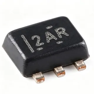
The principal feature is the 1 pF typical capacitance, which helps preserve signal integrity on RF and high-speed lines. The verified data identifies four RF ESD protection diodes in the six-terminal device and describes use for one protected signal line in an anti-parallel configuration. The application example also notes that a protected line may carry superimposed DC voltage up to ±2 × VF, where VF is the diode forward voltage.
Technically, the device combines low capacitance with high transient-energy handling. Its 2-channel arrangement allows two signal conductors or related interface lines to be protected in a compact footprint. The 70 V rating reported for the related distributor listing describes the device category and ordering context, while the verified series document supplies the application example and protection references.
Typical uses include RF antenna inputs, GPS, HDMI, Ethernet interfaces, communications equipment, and ultra-high-speed data-line protection. In these systems, capacitance affects edge bandwidth, insertion loss, and signal integrity; a 1 pF device is selected when the interface must remain responsive while exposed to ESD events.
PCB placement is important. Place the protection device close to the connector or board entry, connect the protected line through the device as shown in the manufacturer application example, and keep high-current surge paths away from sensitive logic. Verify the complete interface against the applicable system ESD, EFT, and surge requirements rather than relying only on the device rating.
This page consolidates the verified Infineon series documentation, distributor information, technical parameters, protection standards, and design considerations for faster component selection and PCB implementation.
直接替換替代品,適用於 ESD1P0RFS — 相同封裝,腳位對腳位相容。需重新設計 PCB 的不同封裝零件不列入。
此系列的變體
與下列產品可直接替換的同系列型號: ESD1P0RFS (相同外形與佔位) — 差異在於 Application Configuration, Device Type, Package, Surge Compliance.
ESD1P0RFS 最大額定值與電氣特性
| Device Type | RF ESD protection diode / transient voltage suppressor diode |
| Number of Channels | 2 channels |
| Number of Diodes | 4 diodes |
| Typical Capacitance | 1 pF |
| ESD Protection, Contact | ±20 kV |
| ESD Standard | IEC61000-4-2 |
| EFT Standard | IEC61000-4-4 |
| EFT Waveform | A, 5/50 ns |
| Surge Standard | IEC61000-4-5 |
| Surge Waveform | A, 8/20 µs |
| Surge Compliance | 10 A |
| 腳位數 | 6 pins |
| Terminal Position | Dual |
| Terminal Form | Gull wing |
| 安裝類型 | Surface mount |
| Package Shape | Rectangular |
| Application Configuration | 1 protected signal line in low-capacitance anti-parallel configuration |
| Allowed Superimposed DC Voltage | Up to ±2 × VF |
| Manufacturer | Infineon Technologies AG |
ESD1P0RFS rectangular 腳位配置指南
ESD1P0RFS(rectangular 封裝)的腳位配置。 此功率元件具有閘極、汲極與源極端子。對於非極性封裝,請參閱製造商資料表以取得確切的第 1 腳方向與佈局詳細資訊。常見應用包括電源設計、馬達驅動與負載切換。

無詳細腳位定義資料: ESD1P0RFS.
請參閱 資料表 以查看完整腳位配置。
典型應用
ESD1P0RFS 適用於 6 應用s: RF Antenna Input Protection, GPS and Navigation Interfaces, HDMI High-Speed Interface Protection, Ethernet Network Port Protection, Ultra-High-Speed Data-Line Protection, Communications Equipment ESD Protection.
RF Antenna Input Protection
The Infineon ESD1P0RFS fits RF antenna-entry protection because its 1 pF typical capacitance minimizes loading on high-frequency signal paths while providing ±20 kV contact ESD protection. Place the diode close to the antenna connector and route the protected conductor through the manufacturer’s anti-parallel arrangement. This helps protect the receiver or RF front end from electrostatic discharge without intentionally adding a large shunt capacitance. The design must still account for connector geometry, RF return paths, and the actual antenna frequency range.
推薦
GPS and Navigation Interfaces
ESD1P0RFS is appropriate for GPS or navigation signal protection where low capacitance helps preserve the protected line’s RF behavior. The verified Infineon documentation associates the ESD1P0RF family with GPS applications and specifies 1 pF typical capacitance. Position the protection device near the connector entry and use a controlled ground return so the transient current does not flow through sensitive receiver traces. Validate the complete interface for RF loss, ESD immunity, and system-level surge requirements.
推薦
HDMI High-Speed Interface Protection
The 1 pF typical capacitance of ESD1P0RFS makes it a candidate for ESD protection on suitable HDMI or other ultra-high-speed data lines. It helps limit parasitic loading while the device diverts ESD transients away from downstream logic. The correct channel assignment and connection must follow the six-terminal package drawing and the interface’s protection architecture. Because the verified data does not provide every pin-level connection or channel-bandwidth detail, engineers should confirm both with the current Infineon datasheet.
推薦
Ethernet Network Port Protection
ESD1P0RFS can be evaluated for Ethernet or other communications interfaces where low capacitance and transient protection are both important. The verified Infineon family page identifies Ethernet-related applications, and the target device provides 1 pF typical capacitance with ±20 kV contact ESD protection. Place the diode at the external interface boundary, maintain a short surge return, and verify line impedance and insertion loss after adding the protection path. A system-level qualification remains necessary.
推薦
Ultra-High-Speed Data-Line Protection
For ultra-high-speed data lines, ESD1P0RFS offers a compact, low-capacitance protection solution with 2-channel capability and 1 pF typical capacitance. The protection device should be close to the connector so the vulnerable PCB segment is minimized. Designers must balance capacitance, data-rate margin, return-path continuity, and the IEC61000-4-2, IEC61000-4-4, and IEC61000-4-5 test objectives. Use the manufacturer’s application example as the starting point, then validate with the finished board.
推薦
Communications Equipment ESD Protection
ESD1P0RFS is suited to communications equipment exposed to user contact or cable-transient ESD events. Its 1 pF typical capacitance is intended to preserve signal behavior in RF and high-speed interface sections, while the ±20 kV contact rating provides a defined device-level protection target. Integrate the diode close to the connector, provide a low-impedance return, and avoid routing transient current through sensitive analog or digital areas. The final device choice should be checked against the enclosure, grounding, and system test standard.
推薦
工程參考資料,適用於 ESD1P0RFS — 比較、設計指引及合規資訊。
選型指南
與替代品比較
| 參數 | 本產品 | ESD1P0RFW |
|---|---|---|
| Package | 6-pin surface-mount gull-wing package | 6-pin surface-mount package; exact package designation requires datasheet confirmation |
| Brand | Infineon | Infineon |
| Channel Count | 2 channels | 1 channel |
| Typical Capacitance | 1 pF | 1 pF |
| Contact ESD Protection | ±20 kV | ±20 kV |
| Surge Compliance | 10 A | 10 A |
| Application Class | RF ESD protection diode | RF ESD protection diode |
| Protection Standards | IEC61000-4-2, IEC61000-4-4, IEC61000-4-5 | IEC61000-4-2 and related transient-protection family ratings |
主要差異化特點
- Two-channel protection in one device (對比ESD1P0RFW)
- Matched low-capacitance RF protection (對比ESD1P0RFW)
- Defined transient-protection coverage (對比ESD1P0RFW)
設計說明
Place ESD1P0RFS at the interface boundary, immediately next to the external connector or cable entry. Route the protected signal through the device according to the Infineon application example and keep the ESD current return short and continuous. A long unprotected trace between the connector and diode leaves the downstream circuit exposed to the transient event.
Use the 1 pF typical capacitance as the initial signal-integrity selection value, then verify the complete interface with the actual connector, trace geometry, receiver impedance, and target data rate. Confirm insertion loss, edge-rate degradation, and return-path behavior on the finished PCB rather than assuming the device capacitance alone guarantees compliance.
Do not substitute ESD1P0RFW without checking channel count and PCB connectivity. The verified family data identifies ESD1P0RFS as 2-channel and ESD1P0RFW as 1-channel, even though both are described with approximately 1 pF capacitance and ±20 kV contact ESD protection. Also verify the six-terminal pin assignment from the official datasheet before fabrication.
合規資訊
The verified data references IEC61000-4-2, IEC61000-4-4, and IEC61000-4-5 transient-protection tests, but it does not state RoHS, REACH, lead-free, halogen-free, AEC-Q100, or conflict-minerals status.