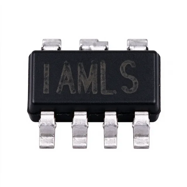
MP2451DJ-LF-Z - 36V, 2MHz, 0.6A Step-Down Converter | MPS
MPN: MP2451DJ-LF-Z ✓ 啟用中| 數量 | 單價 | 小計 |
|---|---|---|
| 1 | $0.5062 | $0.51 |
| 10 | $0.3656 | $3.66 |
| 100 | $0.3234 | $32.34 |
| 500 | $0.3094 | $154.70 |
| 1,000 | $0.2953 | $295.30 |
MP2451DJ-LF-Z 概覽
A step-down switching regulator (also called a buck converter) is a type of switched-mode power supply (SMPS) that efficiently converts a higher DC input voltage to a lower DC output voltage by rapidly switching an internal MOSFET and storing energy in an external inductor. Within the broader power-management hierarchy, the MP2451 sits between DC-DC converters (the family) and synchronous/non-synchronous buck regulators (the sub-family), making it well-suited for point-of-load (POL) rails in space-constrained designs. The 2 MHz switching frequency lets designers use a tiny 1 µH to 4.7 µH inductor, reducing total solution size dramatically versus 500 kHz alternatives.
Key specifications include a 0.6 A continuous output rating, 36 V absolute-maximum input, internal compensation that removes the need for an external compensation network, and built-in protections such as over-current protection (OCP), thermal shutdown, and under-voltage lockout (UVLO). The TSOT-23-6 footprint occupies roughly 2.9 mm × 1.6 mm of board area, making the part one of the smallest 36 V-tolerant synchronous-feel buck regulators on the market. The wide VIN range specifically targets automotive and industrial environments subject to load-dump and cold-crank transients on a 12 V or 24 V bus.
Typical applications include distributed 5 V or 3.3 V POL rails from a 12 V/24 V automotive battery, USB-powered devices, IoT sensors, DSL/cable modems, and portable industrial instrumentation. The combination of high switching frequency and small package also suits FPGA/CPLD auxiliary rails where board area is at a premium and low EMI from forced-CCM operation is desired.
When laying out the PCB, place the input capacitor, the inductor, and the BST bootstrap component as close to the IC as possible and keep the high-current loop minimal. The exposed ground pad under the TSOT-23-6 must be soldered to a sufficient ground copper pour; the part relies on PCB copper for thermal dissipation, so a thermal via array is strongly recommended when delivering close to the 0.6 A rating continuously.
直接替換替代品,適用於 MP2451DJ-LF-Z — 相同封裝,腳位對腳位相容。需重新設計 PCB 的不同封裝零件不列入。
此系列的變體
與下列產品可直接替換的同系列型號: MP2451DJ-LF-Z (相同外形與佔位) — 差異在於 Output Voltage Range, Package, Quiescent Current (Shutdown), RoHS Status, Soft Start.
快速比較工具 — 選擇替代零件進行並排比較:
MP2451DJ-LF-P
聯絡詢價
查看資料表 →TPS62130RGTR
聯絡詢價
查看資料表 →MP2451DT-LF-Z
📋 參考替代品(不在目錄中)
MP2451DT-LF-P
📋 參考替代品(不在目錄中)
MP2451GJ-Z
📋 參考替代品(不在目錄中)
LMR16006XDDCR
📋 參考替代品(不在目錄中)
MP2451DJ-LF-Z 最大額定值與電氣特性
| 拓撲 | Step-Down (Buck) Switching Regulator |
| 輸入電壓範圍 | 3.3 V to 36 V |
| 輸出電壓範圍 | 0.8 V to (VIN - 1 V) adjustable |
| Output Current (Continuous) | 0.6 A (typical) |
| 切換頻率 | 2 MHz (fixed) |
| Switching Control | Current-mode PWM |
| Quiescent Current (Shutdown) | 3 µA (typical) |
| Internal MOSFET | Integrated high-side high-voltage MOSFET |
| 封裝 | TSOT-23-6 (Thin SOT-23-6) |
| 安裝類型 | Surface Mount |
| 軟啟動 | Internal (programmed by BST cap) |
| RoHS 狀態 | Compliant (LF-Z suffix indicates lead-free) |
MP2451DJ-LF-Z 腳位配置
| 腳位 1 | EN — Enable input (high to enable switching) |
| 腳位 2 | GND — Ground / exposed thermal pad connection |
| 腳位 3 | SW — Switch node - connect to external inductor |
| 腳位 4 | IN — Input supply voltage (3.3 V to 36 V) |
| 腳位 5 | BST — Bootstrap capacitor pin for high-side gate drive |
| 腳位 6 | FB — Feedback input to internal error amplifier (set by external divider to 0.8 V internal reference) |
典型應用
MP2451DJ-LF-Z 適用於 6 應用s: Automotive 12V/24V POL Rails, Industrial 24V Sensor and Instrumentation Rails, Portable / Battery-Powered IoT Devices, FPGA / CPLD Auxiliary Supply Rails, USB-Powered Devices and Charging Rails, E-Metering / Smart Energy Sub-Systems.
Automotive 12V/24V POL Rails
The MP2451DJ-LF-Z converts a noisy 12 V or 24 V automotive battery rail into a clean 5 V or 3.3 V supply for body electronics, sensors, and infotainment modules. Its 3.3 V to 36 V input range survives load-dump transients up to 36 V, while the 2 MHz switching frequency keeps the output LC filter footprint tiny enough to fit next to an ECU connector. At 0.6 A continuous output it comfortably drives small MCUs, CAN transceivers, and sensor arrays. The exposed thermal pad of the TSOT-23-6 should be tied to a generous copper pour with thermal vias to dissipate the 1.8 W typical dissipation at VIN=12 V, VOUT=3.3 V, IOUT=0.6 A.
推薦
Industrial 24V Sensor and Instrumentation Rails
The MP2451DJ-LF-Z is ideal for industrial 24 V bus systems that need a tightly regulated 5 V, 3.3 V, or even 1.8 V rail for sensors, op-amps, and isolated data-acquisition front-ends. The wide 3.3 V to 36 V input tolerates 24 V nominal with up to 36 V transient headroom, while the 0.6 A output is more than enough for a strain-gauge bridge, a 4-20 mA loop driver, and a small MCU combined. With internal compensation the design uses only six external components, simplifying agency pre-compliance testing for IEC 61000-4-2/4 surge and burst immunity.
推薦
Portable / Battery-Powered IoT Devices
In battery-powered IoT devices, the MP2451DJ-LF-Z draws only 3 µA in shutdown, allowing the host MCU to power-gate the regulator during sleep cycles and extend battery life from months to years. Stepping down a single-cell Li-ion (3.0 V to 4.2 V) or two AA cells (2.0 V to 3.2 V with boost) to 1.8 V or 3.3 V is well within its 0.8 V to VIN capability. The 0.6 A rating covers LoRa/BLE transmit bursts and the 2 MHz switching frequency lets a 1 µH inductor keep the total solution height under 1.2 mm for wearable form factors.
推薦
FPGA / CPLD Auxiliary Supply Rails
Modern FPGAs and CPLDs require multiple low-voltage rails (1.0 V, 1.2 V, 1.8 V, 2.5 V, 3.3 V) at moderate currents under 0.5 A, which the MP2451DJ-LF-Z supplies easily with its 0.6 A output. The 2 MHz fixed-frequency operation synchronises cleanly with the FPGA's internal clock tree, avoiding low-frequency beat tones that would fail CISPR 22 EMI scans. The TSOT-23-6 footprint fits into the tight area under an FPGA BGA, even on a 4-layer board with 0402 passives. The internal soft-start limits inrush to protect the FPGA's internal clamp diodes at hot-plug events.
推薦
USB-Powered Devices and Charging Rails
USB-powered gadgets typically require a 5 V input handling dropouts to 4.5 V during USB suspend and 5.25 V at full load - well inside the 3.3 V to 36 V window of the MP2451DJ-LF-Z when generating sub-5 V rails. The 0.6 A output covers most single-port USB Type-A applications including charging controllers, status LEDs, and MCU housekeeping. The fixed 2 MHz switching frequency permits a small 2.2 µH inductor that drops neatly into the USB-A connector footprint, while internal EN logic lets a host MCU perform USB-C PD role-swap without glitching downstream rails.
推薦
E-Metering / Smart Energy Sub-Systems
Smart electricity, gas, and water meters need a low-noise, low-quiescent buck regulator that runs directly from the meter's rectified mains or battery-backed 24 V rail. The MP2451DJ-LF-Z's 0.6 A output comfortably powers the meter's MCU, an OLED display driver, and a wireless M-Bus or LoRaWAN modem, while its 36 V input rating tolerates rectified 24 V AC adapters and large capacitive holdup during mains glitches. The 3 µA shutdown current keeps the regulator idle during sleep, preserving battery life on battery-backed metering designs.
推薦
推薦產品摘要
工程參考資料,適用於 MP2451DJ-LF-Z — 比較、設計指引及合規資訊。
選型指南
與替代品比較
| 參數 | 本產品 | MP2451DT-LF-Z | MP2451DJ-LF-P | MP2451GJ-Z | TPS62130RGTR | LMR16006XDDCR |
|---|---|---|---|---|---|---|
| Brand | Monolithic Power Systems | Monolithic Power Systems | Monolithic Power Systems | Monolithic Power Systems | Texas Instruments | Texas Instruments |
| Package | TSOT-23-6 | TSOT-23-6 - same | TSOT-23-6 - same | TSOT-23-6 - same | TSOT-23-6 - same | TSOT-23-6 - same |
| Input Voltage Range | 3.3 V to 36 V | 3.3 V to 36 V | 3.3 V to 36 V | 3.3 V to 36 V | 3 V to 17 V (narrower) | 4 V to 60 V (wider) |
| Output Current | 0.6 A | 0.6 A | 0.6 A | 0.6 A | 3 A (5x higher) | 0.6 A |
| Switching Frequency | 2 MHz | 2 MHz | 2 MHz | 2 MHz | 2.5 MHz | 0.7-2.2 MHz adj |
| Compensation | Internal | Internal | Internal | Internal | Internal | Internal |
| Package Pin Order | EN/GND/SW/IN/BST/FB | EN/GND/SW/IN/BST/FB - identical | EN/GND/SW/IN/BST/FB - identical | EN/GND/SW/IN/BST/FB - identical | EN/PG/SW/IN/BST/FB (PG vs GND differs) | BST/IN/EN/SW/FB/GND (rotated pinout) |
主要差異化特點
- Widest VIN-to-package ratio: 36 V input in TSOT-23-6 (對比LMR16006XDDCR)
- Smallest BOM with 0.6 A/36 V combination (對比TPS62130RGTR)
- Multiple shipping-format options from the same die (對比MP2451DT-LF-Z)
設計說明
Place the input bypass capacitor (typically 1 µF to 4.7 µF ceramic, X7R, 50 V or higher) as close to the IN and GND pins as possible, within 2 mm. Route the SW node away from sensitive analog feedback traces; the high dv/dt on SW couples easily into the FB divider and degrades load regulation. Use a 4-layer PCB with a dedicated ground plane and stitch the input capacitor, IC, and output capacitor grounds with short wide traces or vias directly under the exposed TSOT-23-6 thermal pad.
Estimated: at VIN=12 V, VOUT=3.3 V, IOUT=0.6 A, the regulator dissipates roughly (12 - 3.3) × 0.6 / efficiency = approximately 1.95 W assuming 85% efficiency. The TSOT-23-6 has a theta_JA near 80 °C/W on a 1 oz 2-layer board, so junction temperature rises about 156 °C above ambient - too high for 25 °C ambient. Use at least a 4-layer board with a >50 mm² exposed-pad copper pour and thermal via array (4-6 vias 0.3 mm) to drop theta_JA below 40 °C/W for reliable full-load operation at 85 °C ambient.
Do not omit the BST capacitor (typically 100 nF) between BST and SW - without it the high-side gate drive will lose its supply rail and the part will fail to start. Do not use an inductor saturation current rating lower than the peak current calculated at full load plus 30% margin; undersaturation causes the part to enter OCP prematurely. Avoid using electrolytic capacitors at SW/VOUT - their ESL degrades the high-frequency switching loop and may cause instability. Verify polarity of feedback resistors; reversed divider will produce the maximum output voltage potentially damaging downstream circuitry.
The 2 MHz fixed-frequency switching enables the use of small ceramic input and output capacitors (typically 4.7 µF minimum) and a 1 µH to 4.7 µH inductor, dramatically shrinking the high-current loop. A shielded inductor (Coilcraft XAL series, Würth WE-LHMI) reduces radiated EMI below CISPR 22 / EN 55022 class B limits; a pi-filter on the input further attenuates conducted emissions back to the source. Place the bootstrap capacitor return directly on the SW plane to minimise dV/dt-induced ringing.
合規資訊
LF-Z suffix confirms lead-free / RoHS compliant per MPS conventions. Not AEC-Q100 qualified - automotive AEC-Q100 compliance requires an explicitly automotive-graded variant. REACH compliance inferred from MPS standard reach declaration.






