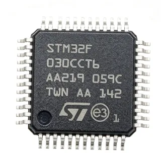
MPC8555PXAPF - PowerQUICC III e500 MPU 833MHz | NXP FCPBGA-783
MPN: MPC8555PXAPF ✗ 停產MPC8555PXAPF 概覽
A microprocessor (MPU) is an integrated circuit that contains the arithmetic, logic, and control circuitry required to execute software instructions and act as the central processing unit of an embedded system. Within the broader taxonomy of semiconductors, the MPC8555PXAPF sits in the integrated communications processor (ICP) category, a hypernym combining microprocessor (MPU), digital signal processor (DSP), and network-on-chip peripherals. PowerQUICC III is NXP's flagship ICP family, specifically engineered to offload packet processing, ATM, Ethernet, and TDM voice/datacom traffic from the host CPU.
Key features include a 32-bit PowerPC e500 core with dual-issue superscalar pipeline, dedicated security engine, integrated DDR memory controller, four Gigabit Ethernet MACs, dual PCI/PCI-X interfaces, and a RapidIO interconnect. The device is built on a 1.2 V core supply with 1.5 V/1.8 V/2.5 V/3.3 V I/O tolerance for legacy peripheral interfacing. The 783-FCPBGA package provides flip-chip interconnect for high signal integrity at the elevated 833 MHz core frequency.
The architecture combines a high-performance e500 core, separate RISC-based peripheral engines, and an integrated security coprocessor. This heterogeneous multiprocessing approach allows wire-speed packet classification, encryption/decryption (IPSec, SSL/TLS), and QoS queue management without burdening the host core. The device delivers deterministic latency for backplane and line-card deployments.
Typical applications include enterprise routers, multiservice access concentrators, DSLAM line cards, wireless base station controllers, industrial protocol gateways, and network-attached storage controllers. The combination of gigabit Ethernet, PCI-X, and RapidIO makes it ideal for high-bandwidth line cards.
When designing with this device, allocate adequate PCB layers (typically 8-10) for the 1 mm-pitch BGA breakout, provide a low-noise power supply tree (separating 1.2 V core from 1.5 V/3.3 V I/O rails), and account for the thermal envelope (junction-to-ambient thermal resistance depends on PCB stack-up and airflow). Reference the NXP application note for DDR termination and impedance-controlled routing.
This page synthesizes distributor pricing, same-package alternatives within the PowerQUICC III family, and practical design notes not consolidated in the manufacturer datasheet.
直接替換替代品,適用於 MPC8555PXAPF — 相同封裝,腳位對腳位相容。需重新設計 PCB 的不同封裝零件不列入。
此系列的變體
與下列產品可直接替換的同系列型號: MPC8555PXAPF (相同外形與佔位) — 差異在於 Data Bus Width, Mounting Type, Package, RoHS Status, Series.
MPC8555EVTAPF
✅ 直接替換聯絡詢價
查看資料表 →MPC8555PXAQF
✅ 直接替換 ⚠️ 規格未經驗證📋 參考替代品(不在目錄中)
MPC8541EPXAPF
✅ 直接替換📋 參考替代品(不在目錄中)
MPC8541PXAQF
✅ 直接替換 ⚠️ 規格未經驗證📋 參考替代品(不在目錄中)
MPC8569CVJAQLJB
✅ 直接替換📋 參考替代品(不在目錄中)
MPC8555PXAPF 最大額定值與電氣特性
| Manufacturer | NXP Semiconductors (formerly Freescale) |
| Series | PowerQUICC III |
| Core Architecture | PowerPC e500 |
| Core Count | 1 |
| 資料匯流排寬度 | 32-bit (64-bit datapath) |
| Core Clock Speed | 833 MHz |
| Core Supply Voltage | 1.2 V |
| I/O Supply Voltage | 1.5 V / 1.8 V / 2.5 V / 3.3 V tolerant |
| 封裝 | 783-FCPBGA (29x29 mm, 1 mm pitch, flip-chip plastic BGA) |
| 安裝類型 | Surface Mount (BGA) |
| 腳位數 | 783 |
| RoHS 狀態 | Compliant (per DigiKey listing) |
| 生命週期狀態 | Not Recommended for New Designs (NRND) |
MPC8555PXAPF 783-fcpbga (29x29 mm, 1 mm pitch, flip-chip plastic bga) 腳位配置指南
MPC8555PXAPF(783-fcpbga (29x29 mm, 1 mm pitch, flip-chip plastic bga) 封裝)的腳位配置。 此數位 IC 包含 GPIO、通訊介面(UART、SPI、I2C)與電源腳位。替代腳位功能與配置選項請參閱製造商資料表。對嵌入式系統設計與 PCB 佈局至關重要。

無詳細腳位定義資料: MPC8555PXAPF.
請參閱 資料表 以查看完整腳位配置。
典型應用
MPC8555PXAPF 適用於 6 應用s: Enterprise Edge Router, DSLAM / GPON Line Card, Wireless Base Station Controller, Network-Attached Storage Controller, Industrial Protocol Gateway, Voice over IP (VoIP) Media Gateway.
Enterprise Edge Router
The MPC8555PXAPF serves as the central processing engine in enterprise edge routers, where its 833 MHz PowerPC e500 core handles control-plane and routing-protocol processing while four integrated tri-speed Ethernet MACs (10/100/1000) terminate multiple WAN/LAN links simultaneously. The RapidIO and PCI-X interfaces allow direct connection to cryptographic accelerator cards or fabric switches, while the DDR controller with ECC maintains a fast routing table database. Compared with discrete CPU + bridge-chip designs, the MPC8555PXAPF reduces BOM and PCB area while sustaining wire-speed packet throughput on line cards. The 783-FCPBGA package supports the multi-gigabit data flow and the high I/O count needed for multi-port routers.
推薦
DSLAM / GPON Line Card
In DSLAM (Digital Subscriber Line Access Multiplexer) and GPON (Gigabit Passive Optical Network) line cards, the MPC8555PXAPF aggregates traffic from many subscriber lines, performs packet classification, and forwards data upstream. The device's dedicated communications processor module handles ATM/TDM segmentation and reassembly without burdening the e500 core, freeing it for QoS and traffic shaping. The four gigabit Ethernet MACs and PCI-X interfaces connect to PHY transceivers and backplane fabrics. At 833 MHz, the device sustains per-line bandwidth shaping and IGMP snooping for IPTV multicast streams, ensuring low latency across hundreds of subscribers per card.
推薦
Wireless Base Station Controller
For 3G/UMTS base station controllers, the MPC8555PXAPF handles the Iub interface between the radio network controller (RNC) and Node B, executing layer-2 protocols, frame segmentation, and ATM Adaptation Layer 2 (AAL2) processing. The 833 MHz e500 core and integrated CPM together meet the throughput demands of multiple 3GPP carriers, while the security engine variant (MPC8555EVTAPF) provides hardware-accelerated Kasumi encryption for cellular confidentiality. Dual PCI-X interfaces connect to DSP cards, and the DDR controller supports the large buffer pools required for HS-DPA aggregation.
推薦
Network-Attached Storage Controller
In mid-range NAS controllers, the MPC8555PXAPF runs a storage management OS while coordinating four gigabit Ethernet ports for link aggregation or MPIO. The DDR memory controller with ECC supports RAM-based read/write caches, and the local bus unit connects to flash (NOR for boot, NAND for storage firmware). The PCI-X interface links to SAS/SATA controllers for HDD shelves. Compared with general-purpose x86 NAS controllers, the PowerQUICC III architecture delivers lower power consumption and deterministic latency, well-suited to small/medium business file-serving appliances.
推薦
Industrial Protocol Gateway
The MPC8555PXAPF converts between industrial protocols (EtherCAT, PROFINET, Modbus/TCP, EtherNet/IP) and legacy fieldbus (Profibus, CANopen) in industrial automation. The dual UARTs serve RS-485/RS-232 legacy fieldbus, while the four Ethernet MACs handle multi-protocol industrial Ethernet. The wide operating temperature range and BGA package suit harsh-environment panels. Hardware TCP/IP offload via CPM reduces protocol latency, and DDR with ECC supports deterministic real-time response critical for closed-loop motion control.
推薦
Voice over IP (VoIP) Media Gateway
In carrier-grade VoIP media gateways, the MPC8555PXAPF performs RTP packetization, jitter buffering, codec transcoding (G.711/G.729/G.722), and SIP/H.323 signaling at gigabit line rate. The serial TDM interfaces connect to legacy PSTN T1/E1 spans, while Ethernet MACs terminate IP uplinks. Hardware encryption (SEC engine on the EV variant) secures SRTP/TLS media streams. The 833 MHz core handles tens of thousands of simultaneous voice channels per device with deterministic latency, making it a cost-effective alternative to DSP farms.
推薦
推薦產品摘要
工程參考資料,適用於 MPC8555PXAPF — 比較、設計指引及合規資訊。
選型指南
與替代品比較
| 參數 | 本產品 | MPC8555EVTAPF | MPC8555PXAQF | MPC8541EPXAPF | MPC8569CVJAQLJB |
|---|---|---|---|---|---|
| Brand | NXP Semiconductors | NXP Semiconductors | NXP Semiconductors | NXP Semiconductors | NXP Semiconductors |
| Package | 783-FCPBGA (29x29) | 783-FCPBGA (29x29) - same | 783-FCPBGA (29x29) - same | 783-FCPBGA (29x29) - same | 783-FCPBGA (29x29) - same |
| Core Frequency | 833 MHz | 833 MHz | 833 MHz | 833 MHz | 1.33 GHz |
| Security Engine (SEC) | No | Yes (SEC 3.0) | No | Yes (SEC 2.0) | Yes (SEC 4.0) |
| Dedicated CPM | Yes | Yes | Yes | No | Yes |
| Ethernet MACs | 4 (tri-speed) | 4 (tri-speed) | 4 (tri-speed) | 3 (tri-speed) | 8 (1/10G capable) |
| DDR Memory Controller | 64-bit DDR/DDR2 | 64-bit DDR/DDR2 | 64-bit DDR/DDR2 | 64-bit DDR/DDR2 | 64-bit DDR2/DDR3 |
| Temperature Grade | Commercial (AP) | Commercial (AP) | Extended Industrial (AQ) | Commercial (AP) | Extended (ALJB) |
| Lifecycle Status | NRND | NRND | NRND | NRND | Active |
主要差異化特點
- Broader peripheral integration than MPC8541E variant (對比MPC8541EPXAPF)
- Lower cost than SEC-enabled variant (對比MPC8555EVTAPF)
- Lower core frequency than MPC8569 successor (對比MPC8569CVJAQLJB)
- Commercial vs extended temperature grades (對比MPC8555PXAQF)
設計說明
Estimated: The 783-ball FCPBGA at 1 mm pitch on 29x29 mm body requires a minimum of 8 PCB layers for fanout, with microvia-in-pad or laser-drilled vias recommended for the inner ball rows. Use a controlled-impedance stack-up (50 ohm single-ended, 100 ohm differential) for Ethernet and RapidIO traces, and keep the DDR trace length matched within 25 mils per byte lane. Reference NXP application note AN2664 for the recommended MPC8555 layout stack-up.
At maximum core frequency (833 MHz) with full peripheral utilization, the MPC8555PXAPF typically dissipates 4-7 W. The thermal resistance theta_JA for the 783-FCPBGA on a standard 8-layer JEDEC test board is approximately 15-20 C/W with adequate airflow. A thermal pad area below the package should be soldered to the PCB with thermal vias to the inner ground plane. Forced-air cooling (200 LFM minimum) is recommended for closed enclosures. Reference NXP MPC8555E hardware specifications for the exact thermal envelope.
The MPC8555PXAPF requires a multi-rail power supply: VCORE at 1.2 V (estimated ~3-5 A peak), VDD I/O at 1.5 V/1.8 V/2.5 V/3.3 V (estimated ~1-2 A depending on load), and AVCC for the PLL at 1.2 V. Use a PMIC (e.g., NXP MMPF0100) with sequenced startup to ensure VCORE comes up before I/O rails. Decoupling requires bulk capacitors (47 uF or higher) at each supply pin plus 100 nF and 10 nF ceramics at high-frequency pins. Inductor selection for switchers must meet the 833 MHz core transient response.
Do not assume firmware portability from MPC8240/MPC8260/MPC8560 to MPC8555 - the e500 core requires a recompiled kernel, boot ROM must be re-generated, and U-Boot/UEFI must be re-validated. JTAG trace pins must be brought out for boundary-scan and debug. The DDR controller must be calibrated for the chosen PCB trace lengths before relying on the system for production. Always verify the errata document from NXP before locking firmware.
Place the DDR SDRAM chips as close as possible to the MPC8555PXAPF (under 3 cm total trace length), with each byte lane matched to within 25 mils. The four Ethernet MACs each require a 1:1 center-tap transformer to magnetics; do not share ground between analog and digital sections of the PHY rails. The PCI-X interface requires 100 MHz reference clock with 100 ppm tolerance and a source-impedance matched clock trace.
合規資訊
RoHS compliance confirmed per DigiKey product listing (2026-10-16). REACH SVHC declaration should be requested from NXP directly. AEC-Q100 not applicable (telecom/networking IC, not automotive).