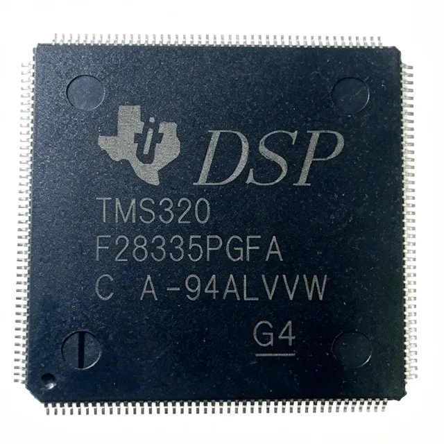
TMS320F28335PGFA - 150MHz 32-bit C2000 DSC MCU | Texas Instruments
MPN: TMS320F28335PGFA ✓ 啟用中TMS320F28335PGFA 概覽
A digital signal controller combines the real-time control capability of a microcontroller (MCU) with the mathematical throughput of a digital signal processor (DSP). Within the embedded control hierarchy, the C2000 Delfino DSC sits at the top of real-time controllers, above generic MCUs, for closed-loop control loops running at tens of kilohertz. The C28x core uses a Harvard architecture with a hardware multiplier and a single-precision floating-point unit (FPU) that accelerates field-oriented control (FOC) and other complex control algorithms.
Key features include a 12-bit ADC with up to 16 channels, 18 PWM outputs including high-resolution PWM (HRPWM), and communication peripherals covering CAN, SPI, SCI (UART), and I2C. An external memory interface (EMIF) expands memory beyond on-chip resources, a differentiator versus smaller C2000 parts such as the TMS320F28027.
The device is fabricated on TI 180 nm CMOS process technology. It runs from a 1.9 V core supply and 3.3 V I/O supply, with typical power consumption near 300 mW at full speed, and operates from -40C to +85C, qualifying it for industrial environments. The FPU executes single-cycle floating-point operations, critical for high-speed control loops without fixed-point IQmath conversion.
Typical applications include servo motor drives, solar inverters, digital power supplies, and industrial automation where fast ADC sampling and precise PWM edges are essential.
Design consideration: decouple the 1.9 V core and 3.3 V I/O rails separately, budget for LQFP thermal dissipation, and use the JTAG port with Code Composer Studio for real-time emulation and debugging.
This page synthesizes distributor pricing, verified drop-in alternatives, and practical design notes not found in the manufacturer datasheet alone.
直接替換替代品,適用於 TMS320F28335PGFA — 相同封裝,腳位對腳位相容。需重新設計 PCB 的不同封裝零件不列入。
此系列的變體
與下列產品可直接替換的同系列型號: TMS320F28335PGFA (相同外形與佔位) — 差異在於 Package, Core Processor, ADC Resolution, External Memory Interface, Flash Memory.
TMS320F28335PTPQ
✅ 直接替換聯絡詢價
查看資料表 →TMS320F28335QPGFAQ1
✅ 直接替換聯絡詢價
查看資料表 →TMS320F28334PGFA
✅ 直接替換 ⚠️ 規格未經驗證📋 參考替代品(不在目錄中)
TMS320F28332PGFA
✅ 直接替換 ⚠️ 規格未經驗證📋 參考替代品(不在目錄中)
TMS320F28335PGFA-N
✅ 直接替換 ⚠️ 規格未經驗證📋 參考替代品(不在目錄中)
TMS320F28335PGFA 最大額定值與電氣特性
| Core | C28x (C2000 Delfino) |
| 資料匯流排寬度 | 32 bit |
| 最大時脈頻率 | 150 MHz (150 MIPS) |
| Floating-Point Unit | Yes (single-precision FPU) |
| Flash Memory | 512 KB (256K x 16) |
| SRAM | 68 KB |
| ADC Resolution | 12 bit |
| ADC Channels | up to 16 |
| PWM Outputs | 18 (including HRPWM) |
| Communication Interfaces | CAN, SPI, SCI (UART), I2C, McBSP |
| External Memory Interface | EMIF |
| Core Supply Voltage | 1.9 V |
| I/O Supply Voltage | 3.3 V |
| Typical Power Consumption | approx. 300 mW at full speed |
| 工作溫度 | -40C to +85C |
| 封裝 | 176-LQFP (24x24 mm, PGF) |
| 安裝類型 | Surface Mount |
| Process Technology | TI 180 nm static CMOS |
TMS320F28335PGFA 176-lqfp (24x24 mm, pgf) 腳位配置指南
TMS320F28335PGFA(176-lqfp (24x24 mm, pgf) 封裝)的腳位配置。 此數位 IC 包含 GPIO、通訊介面(UART、SPI、I2C)與電源腳位。替代腳位功能與配置選項請參閱製造商資料表。對嵌入式系統設計與 PCB 佈局至關重要。

無詳細腳位定義資料: TMS320F28335PGFA.
請參閱 資料表 以查看完整腳位配置。
典型應用
TMS320F28335PGFA 適用於 6 應用s: Servo Motor Drives, Solar Inverters and Digital Power, Industrial Automation and PLCs, Electric Vehicle and Transportation Powertrain, Uninterruptible Power Supplies (UPS), Sensing and Signal Processing Systems.
Servo Motor Drives
The TMS320F28335PGFA fits servo drives because its 150 MHz C28x core with single-precision FPU executes field-oriented control (FOC) loops at 10-20 kHz without IQmath fixed-point overhead. Its 18 PWM outputs with high-resolution PWM (HRPWM) deliver sub-nanosecond edge resolution for current-loop control, while the 12-bit ADC samples phase currents and encoder feedback with minimal latency. In a typical topology, the DSC runs current, velocity, and position cascaded loops, with the FPU accelerating Park/Clarke transforms and PI regulators. The on-chip CAN bus links the drive to PLCs, and the EMIF can buffer multi-axis motion profiles. Compared to fixed-point predecessors, floating-point execution shortens development time and improves numeric stability at full 150 MIPS throughput.
推薦
Solar Inverters and Digital Power
For solar inverters and digital power supplies, the TMS320F28335PGFA provides the real-time control backbone: MPPT algorithms, DC-bus regulation, and grid-synchronization (PLL) loops all run on the 150 MHz FPU-equipped C28x core. The 12-channel 12-bit ADC samples PV voltage/current and grid waveforms, and 18 PWM outputs drive boost and inverter stages with HRPWM precision that reduces harmonic distortion. Its EMIF supports external memory for logging and communication stacks, while on-chip CAN and SCI interfaces connect to monitoring systems. TI explicitly targets solar inverters and digital power with the C2000 Delfino family. Designers should budget the PWM dead-time against the HRPWM resolution and use the ADC early-interrupt feature to synchronize sampling with PWM switching events for lowest current ripple.
推薦
Industrial Automation and PLCs
In industrial automation, the TMS320F28335PGFA serves as a high-performance control node where deterministic closed-loop control meets communication. Its CAN peripheral interfaces with factory networks, SCI/I2C handle sensor and HMI links, and the 150 MHz core performs protocol handling plus fast control math concurrently. The -40C to +85C industrial temperature rating suits cabinet-mounted controllers, and the 512 KB flash holds large application code with field-updatable firmware. Where C2000-class control precision is needed for hydraulics, CNC axes, or test rigs, the Delfino FPU delivers float math without extra fixed-point engineering. Pair it with isolated transceivers and external ADC front-ends when channel counts exceed the 16-channel on-chip ADC; use the EMIF to extend RAM for data logging.
推薦
Electric Vehicle and Transportation Powertrain
Electric-vehicle traction and auxiliary inverter designs benefit from the TMS320F28335PGFA's combination of floating-point FOC capability and high-resolution PWM. The 150 MHz core executes torque control and field-weakening routines, the 12-bit ADC samples motor phase currents synchronized to PWM, and 18 PWM channels cover three-phase bridges plus DC/DC converters. The 512 KB flash supports motor parameter identification and functional-safety-adjacent monitoring code, while CAN connects to the vehicle bus. For production EV programs, the drop-in TMS320F28335QPGFAQ1 variant provides AEC-Q100 qualification on the same footprint, enabling a seamless qualification path from prototype PGFA silicon to automotive-grade parts without PCB redesign. Verify core-voltage sequencing against the battery-supplied 12 V rail using a supervisor IC.
推薦
Uninterruptible Power Supplies (UPS)
Online double-conversion UPS systems use the TMS320F28335PGFA to run rectifier, battery-converter, and inverter control loops simultaneously on one 150 MHz C28x core. The FPU handles sinusoidal reference generation and instantaneous voltage regulation, HRPWM minimizes output THD at 20-50 kHz switching frequencies, and the 16-channel 12-bit ADC multiplexes AC input/output sensing, battery current, and temperature inputs. The 512 KB flash accommodates power-management firmware plus communication (CAN/SCI) stacks for network UPS management. Compared with a separate MCU plus DSP architecture, this DSC consolidates control into one device, reducing BOM cost and loop latency. Designers should isolate the ADC front-end from the power stage with isolated amplifiers and use the PWM trip-zone hardware for cycle-by-cycle overcurrent protection.
推薦
Sensing and Signal Processing Systems
TI positions the C2000 family for sensing and signal processing alongside control, and the TMS320F28335PGFA delivers this with its 12-bit, 16-channel ADC and 150 MIPS core for filtering, FFT-based diagnostics, and sensor fusion at the edge. Vibration monitoring, condition-based maintenance nodes, and intelligent sensor hubs use the FPU for running floating-point filters and transforms in real time, streaming results over CAN, SPI, or SCI. The EMIF supports external memory expansion for buffering long capture windows, and the 68 KB SRAM holds double-buffered acquisition data. Compared with generic MCUs, the deterministic C28x pipeline guarantees sample-to-output latency, which matters for protection-class sensing. Use DMA-driven ADC transfers to keep CPU load low and reserve the eCAP peripherals for timestamped event capture.
推薦
推薦產品摘要
工程參考資料,適用於 TMS320F28335PGFA — 比較、設計指引及合規資訊。
選型指南
與替代品比較
| 參數 | 本產品 | TMS320F28335PTPQ | TMS320F28335QPGFAQ1 | TMS320F28334PGFA | TMS320F28332PGFA |
|---|---|---|---|---|---|
| Package | 176-LQFP (24x24 mm) | 176-LQFP (24x24 mm) - same | 176-LQFP (24x24 mm) - same | 176-LQFP (24x24 mm) - same | 176-LQFP (24x24 mm) - same |
| Brand | Texas Instruments | Texas Instruments | Texas Instruments | Texas Instruments | Texas Instruments |
| Clock Frequency | 150 MHz | 150 MHz | 150 MHz | 150 MHz | 150 MHz |
| Flash Memory | 512 KB (256K x 16) | 512 KB (256K x 16) | 512 KB (256K x 16) | 512 KB (256K x 16) | 256 KB (128K x 16) |
| Floating-Point Unit | Yes (single-precision) | Yes (single-precision) | Yes (single-precision) | Yes (single-precision) | Yes (single-precision) |
| Operating Temperature | -40C to +85C | -40C to +125C | -40C to +125C (AEC-Q100) | -40C to +85C | -40C to +85C |
| External Memory Interface (EMIF) | Yes | Yes | Yes | Yes | Yes |
| Automotive Qualification | No | No | Yes (AEC-Q100) | No | No |
主要差異化特點
- Native single-precision FPU at 150 MHz (對比TMS320F28027PTT)
- External memory interface (EMIF) (對比TMS320F28066PNT)
- Largest flash in the F2833x pin-compatible family (對比TMS320F28332PGFA)
- Automotive drop-in path available (對比TMS320F28335QPGFAQ1)
設計說明
The TMS320F28335PGFA needs two regulated rails: 1.9 V core and 3.3 V I/O. Estimated: at approximately 300 mW total full-speed power, core current is roughly 100-150 mA plus I/O switching current, so a 500 mA LDO per rail has margin. Respect TI's power-up sequencing (VDDIO/VDD before VDD1A18/VDD2A18 analog rails) per the TMS320F2833x datasheet to avoid latch-up; use a supply supervisor or sequencing LDO pair. Place 0.1 uF ceramics at every VDD pin pair plus one 10 uF bulk per rail.
Route the 1.9 V core plane as a tight pour under the 176-LQFP and keep the 3.3 V I/O ring separate; do not share return paths between PWM outputs and the analog ADC front-end. Connect the ADC's analog ground to a quiet star point and add an RC filter (e.g., 10 ohm + 1 uF) on VDDA2/VSSA2 analog supply per TI reference designs (TMDXCNCD28335 ControlCARD layout is a proven pattern). Keep crystal and XCLKOUT traces short and guard with ground.
Three frequent mistakes with this device: (1) leaving XCLKOUT enabled on an unused pin causes EMI - disable it via XCLKOUTDIV register; (2) forgetting pull-up/pull-down configuration on GPIO muxed pins during boot can corrupt boot-mode selection from GPIO84-87; (3) ADC results read without waiting for the end-of-conversion interrupt are stale - always synchronize sampling to PWM via the ePWM SOC trigger. Also verify code-security zone settings before locking the CSM, or JTAG debug access will be permanently lost.
Estimated: at 300 mW typical dissipation in the 176-LQFP (24x24 mm) with theta_JA on the order of 30-40 C/W for a 4-layer board, junction temperature rise is roughly 10-12 C above ambient - no heatsink is needed at full 150 MHz operation. However, if the EMIF drives a heavy external bus at high frequency, I/O switching current rises; verify with TI's power estimation spreadsheet and maintain ambient below +85C for the PGFA suffix.
合規資訊
DigiKey lists the part under green/RoHS packaging (TI 'PGF' packages are lead-free green). AEC-Q100 qualification is available only on the TMS320F28335QPGFAQ1 variant. Detailed REACH and conflict-minerals status: verify on TI product page.







