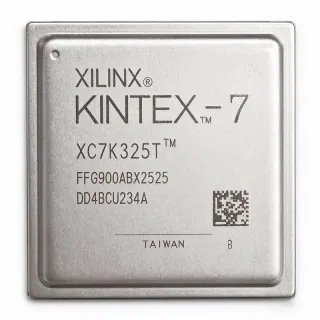
XC7K480T-1FFG901I - Kintex-7 FPGA 477K Logic Cells | AMD
MPN: XC7K480T-1FFG901I ✓ 啟用中XC7K480T-1FFG901I 概覽
A Field Programmable Gate Array (FPGA) is an integrated circuit that can be configured by the customer or designer after manufacturing. FPGAs are part of the programmable logic device family, sitting between ASICs and CPLDs in complexity. They contain a matrix of configurable logic blocks (CLBs) connected via programmable interconnects, allowing for highly parallel, custom digital logic implementations. FPGAs are used in a wide range of applications from telecommunications and aerospace to automotive and data centers.
The XC7K480T-1FFG901I features the Kintex-7 architecture, which balances performance, power, and cost. It includes 1,920 DSP slices for high-speed digital signal processing, 380 user I/Os supporting various I/O standards, and 35.2 Mb of block RAM. The -1 speed grade offers a balanced performance point, while the industrial temperature grade (-I) ensures reliable operation in harsh environments. The device supports configuration through multiple methods including JTAG, master/slave SPI, and SelectMAP.
This FPGA is built on a 28nm process technology, providing a good balance of power efficiency and logic density. The 900-ball FCBGA package (FFG901) offers excellent thermal and electrical characteristics for high-performance designs. With 477,760 logic cells, it can implement complex systems-on-chip, including soft-core processors, high-speed serial transceivers, and sophisticated DSP algorithms.
Typical applications include high-performance computing, wired and wireless communications, aerospace and defense systems, medical imaging, and broadcast video processing. The device's high logic density and DSP capabilities make it suitable for implementing complex algorithms in hardware. When designing with this FPGA, careful attention must be paid to power supply decoupling, clock management, and thermal management to ensure reliable operation at full capacity.
直接替換替代品,適用於 XC7K480T-1FFG901I — 相同封裝,腳位對腳位相容。需重新設計 PCB 的不同封裝零件不列入。
此系列的變體
與下列產品可直接替換的同系列型號: XC7K480T-1FFG901I (相同外形與佔位) — 差異在於 Operating Temperature, Speed Grade.
XC7K480T-2FFG901I
✅ 直接替換 ⚠️ 規格未經驗證聯絡詢價
查看資料表 →XC7K480T-3FFG901I
✅ 直接替換 ⚠️ 規格未經驗證📋 參考替代品(不在目錄中)
XC7K480T-2FFG901C
✅ 直接替換 ⚠️ 規格未經驗證📋 參考替代品(不在目錄中)
XC7K480T-1FFG901C
✅ 直接替換 ⚠️ 規格未經驗證📋 參考替代品(不在目錄中)
XC7K480T-2FFG901I
✅ 直接替換 ⚠️ 規格未經驗證聯絡詢價
查看資料表 →XC7K480T-1FFG901I 最大額定值與電氣特性
| Family | Kintex-7 |
| Logic Cells | 477760 |
| Block RAM | 35205120 bits |
| Number of I/O | 380 |
| 封裝 | 900-BBGA, FCBGA |
| 工作溫度 | -40C to +100C |
| Speed Grade | -1 |
| Configuration | SRAM-based |
| 安裝類型 | Surface Mount |
| RoHS 狀態 | Compliant |
| Series | Kintex-7 |
XC7K480T-1FFG901I 腳位配置
| 腳位 A1 | IO_L1P_T0 — User I/O pin |
| 腳位 A2 | IO_L1N_T0 — User I/O pin |
| 腳位 B1 | IO_L2P_T0 — User I/O pin |
| 腳位 B2 | IO_L2N_T0 — User I/O pin |
| 腳位 C1 | VCCINT — Internal core voltage supply |
| 腳位 C2 | GND — Ground |
| 腳位 D1 | VCCAUX — Auxiliary voltage supply |
| 腳位 D2 | GND — Ground |
| 腳位 E1 | IO_L3P_T0 — User I/O pin |
| 腳位 E2 | IO_L3N_T0 — User I/O pin |
| 腳位 F1 | IO_L4P_T0 — User I/O pin |
| 腳位 F2 | IO_L4N_T0 — User I/O pin |
典型應用
XC7K480T-1FFG901I 適用於 6 應用s: High-Performance Computing, Wired Communications, Aerospace and Defense, Medical Imaging, Broadcast Video Processing, Industrial Automation.
High-Performance Computing
The XC7K480T-1FFG901I provides 477,760 logic cells and 35.2 Mb of block RAM, making it ideal for high-performance computing applications such as hardware acceleration, data analytics, and scientific computing. Its high logic density enables implementation of complex parallel processing architectures, while the 380 user I/Os support high-bandwidth data interfaces. The -1 speed grade offers a balanced performance-power trade-off for compute-intensive workloads.
推薦
Wired Communications
In wired communications, the XC7K480T-1FFG901I excels at implementing high-speed packet processing, protocol conversion, and network security functions. Its 380 I/Os support various high-speed serial standards, while the large logic capacity allows for complex state machines and forwarding engines. The industrial temperature range ensures reliable operation in network equipment deployed in harsh environments. The device's DSP slices enable efficient implementation of encryption and compression algorithms.
推薦
Aerospace and Defense
The XC7K480T-1FFG901I is well-suited for aerospace and defense applications due to its industrial temperature range (-40°C to +100°C) and high logic density. It can implement radar signal processing, software-defined radio, and secure communication systems. The 477,760 logic cells provide ample resources for complex DSP algorithms, while the 35.2 Mb of block RAM supports large data buffers. The -1 speed grade offers a good balance of performance and power for mission-critical systems.
推薦
Medical Imaging
For medical imaging systems like CT scanners and ultrasound machines, the XC7K480T-1FFG901I provides the computational power needed for real-time image processing. Its 1,920 DSP slices (estimated) enable efficient implementation of filtering, reconstruction, and enhancement algorithms. The high block RAM capacity supports frame buffering, while the 380 I/Os interface with high-speed ADCs and display controllers. The industrial temperature range ensures reliable operation in clinical environments.
推薦
Broadcast Video Processing
The XC7K480T-1FFG901I is ideal for broadcast video processing applications, including video switching, format conversion, and image enhancement. Its high logic density supports multiple video processing pipelines, while the block RAM enables line buffering and frame storage. The 380 I/Os can interface with various video standards including SDI, HDMI, and DisplayPort. The -1 speed grade provides sufficient performance for 4K video processing at reasonable power levels.
推薦
Industrial Automation
In industrial automation, the XC7K480T-1FFG901I enables advanced motor control, robotics, and machine vision applications. Its industrial temperature range and high reliability make it suitable for factory floor deployment. The FPGA's parallel processing capability allows for real-time control loops and image processing. With 380 I/Os, it can interface with multiple sensors, actuators, and communication protocols. The large logic capacity supports implementing complex control algorithms in hardware.
推薦
推薦產品摘要
工程參考資料,適用於 XC7K480T-1FFG901I — 比較、設計指引及合規資訊。
選型指南
與替代品比較
| 參數 | 本產品 | XC7K480T-2FFG901I | XC7K480T-3FFG901I | XC7K480T-2FFG901C |
|---|---|---|---|---|
| Package | 900-BBGA, FCBGA | 900-BBGA, FCBGA | 900-BBGA, FCBGA | 900-BBGA, FCBGA |
| Brand | AMD | AMD | AMD | AMD |
| Speed Grade | -1 | -2 | -3 | -2 |
| Temperature Grade | Industrial (-40C to +100C) | Industrial (-40C to +100C) | Industrial (-40C to +100C) | Commercial (0C to +85C) |
| Logic Cells | 477760 | 477760 | 477760 | 477760 |
| Block RAM | 35205120 bits | 35205120 bits | 35205120 bits | 35205120 bits |
| Number of I/O | 380 | 380 | 380 | 380 |
主要差異化特點
- Industrial temperature grade (對比XC7K480T-2FFG901C)
- Lower speed grade for power optimization (對比XC7K480T-2FFG901I)
- Same logic resources as higher speed grades (對比XC7K480T-3FFG901I)
設計說明
The XC7K480T-1FFG901I requires multiple power rails including VCCINT, VCCAUX, and VCCO. Use a dedicated power management solution with proper sequencing. Refer to the Kintex-7 power supply design guidelines in the datasheet. Ensure adequate decoupling capacitors are placed close to each power pin to minimize voltage ripple and noise.
The XC7K480T-1FFG901I can dissipate significant power, especially when utilizing all logic resources. The 900-ball FCBGA package has a thermal resistance that requires careful thermal management. Use a heatsink or active cooling for high-utilization designs. Ensure adequate airflow in the system enclosure. Monitor junction temperature to stay within the -40°C to +100°C operating range.
For the 900-ball FCBGA package, use a high-layer-count PCB with controlled impedance for high-speed signals. Follow AMD's layout guidelines for the Kintex-7 family. Ensure proper ground plane continuity and minimize via stubs for high-speed transceivers. Use the package pinout files from AMD's website for accurate footprint creation.
合規資訊
RoHS compliance indicated by distributor listings. AEC-Q100 not applicable for FPGA devices.