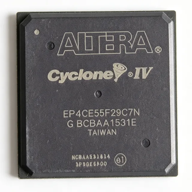
EP4CE55F23I8LN
EP4CE55F23I8LN - 55K FPGA, 484-BGA | Altera | Embedded Logic
Altera EP4CE55F23I8LN is a Cyclone IV E field-programmable gate array with 55,856 logic elements, 2,396,160 bits of embedded memory, and 324 maximum user I/O pins. The device is fabricated using a 60 nm process and is supplied in a 484-ball plastic/epoxy BGA package identified as F23/484-BGA. The verified ordering-code details identify an industrial temperature-grade device, while exact supported I/O standards, logic-element count nomenclature, and configuration features should be confirmed in the current manufacturer ordering information.
A field-programmable gate array is a semiconductor device containing programmable logic blocks, programmable interconnects, and configurable I/O cells. Unlike a fixed-function application-specific integrated circuit, an FPGA can be configured after manufacturing to implement combinational logic, sequential state machines, interfaces, digital signal processing, and bus controllers. Within the semiconductor hierarchy, it belongs to programmable logic, then digital logic, then integrated circuits. Cyclone IV E devices are positioned as low-cost, low-power FPGAs for high-volume and cost-sensitive systems.
The headline capacity of EP4CE55F23I8LN includes 55,856 logic elements, 2,396,160 bits of embedded memory, and 324 maximum user I/O pins. The 60 nm process and 1.2 V supply value are reported in the supplied specification data. The 484-BGA package provides a high-density surface-mount interface for complex designs, but its fine-pitch ball array requires controlled PCB fabrication, assembly, inspection, and power-delivery design. The MPN suffix I8 indicates the industrial ordering variant, although complete electrical and environmental limits are not included in the provided snippets.
Cyclone IV E architecture is suitable for designs requiring flexible logic, embedded memory blocks, configurable I/O, and hardware parallelism. The device can implement custom bridges, control logic, test fixtures, and low-to-moderate throughput signal processing without requiring a mask revision. The supplied data does not expose operating frequency, transceiver count, block RAM organization, phase-locked-loop count, or exact I/O bank assignments; those values are marked as needed elsewhere rather than inferred from the family name.
Typical applications include industrial control and automation, communications infrastructure, video or image-interface bridging, test and measurement equipment, and custom embedded controllers. Its 55,856 logic elements provide capacity for parallel datapaths and multiple peripheral controllers, while 324 maximum user I/O pins support wide external interfaces. Designers must partition logic carefully, verify memory and timing resources, and confirm that the selected package, ball map, configuration interface, and I/O voltage requirements match the PCB.
A primary design trade-off is density versus verification effort. Increasing FPGA utilization can improve integration, but reduces timing margin, routing freedom, power headroom, and design headroom. Review the manufacturer documentation, Intel/Altera device-support resources, configuration schematic, and PCB escape routing before release to fabrication. The exact package drawing and full pinout should be taken from the manufacturer data because the provided web data confirms 484 balls but does not provide a reliable per-ball table.
This page combines verified MPN capacity, package, process, memory, I/O, stock, and datasheet information with application guidance, selection constraints, and a drop-in-alternative review. It distinguishes the 484-BGA EP4CE55F23I8LN from parts with different packages, densities, temperature grades, or speed grades that cannot safely be treated as direct replacements.
询价
联系我们