Microchip Technology

A3P600-1FGG484I - 600K Gate Flash FPGA 235 I/O | Microchip

料号: A3P600-1FGG484I ✓ 量产中
有现货 1-3 个工作日内发货
1.5 V Vdss 484-ball FBGA (FGG484) Package -1 Speed On-chip flash (nonvolatile, single chip) Memory
低至 $79.6 USD / 件
最小起订量: 1 |
价格更新于: 2026-09-01
批量定价
数量 单价 小计
1 $118.5 $118.50
10 $108.2 $1,082.00
100 $96.4 $9,640.00
500 $87.9 $43,950.00
1,000 $79.6 $79,600.00
ℹ️ 所有价格均以 USD 计价

A3P600-1FGG484I 概述

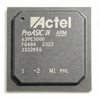
The Microchip Technology (formerly Actel/Microsemi) A3P600-1FGG484I is a 600,000-system-gate ProASIC3 flash-based FPGA with 13,824 VersaTiles (D-flip-flop building blocks), 235 user I/Os, and a -1 speed grade, housed in a 484-ball Fine-Pitch Ball Grid Array (FBGA) package with industrial temperature rating.

A flash-based FPGA is a type of field-programmable gate array that stores its configuration in on-chip flash memory cells rather than SRAM backed by an external configuration device. Within the programmable logic hierarchy, the A3P600 sits at the mid-density tier of the ProASIC3 family between the A3P400 and A3P1000, and as a nonvolatile device it belongs to the broader class of single-chip, live-reprogrammable power management... correction: programmable logic devices that boot instantly at power-up without a bootloader or external configuration flash.

Key features include single-chip nonvolatile operation that eliminates the external configuration PROM required by SRAM FPGAs, a 1.5V core voltage fabricated on a 130nm flash process, support for performance up to approximately 231 MHz system speed on this speed grade, and four I/O banks with independently supplyable VCCIB rails so mixed-voltage I/O standards can coexist on one device.

Technically, ProASIC3 uses the VersaTile architecture, in which every tile can act as a three-input lookup table, a D-flip-flop, or latching element, and the fabric is configured by charge-trapping flash cells. This yields instant-on behavior, low static power, and inherent security because the bitstream is never exposed on an external bus.

Typical applications include industrial automation control, military and aerospace subsystems, medical instrumentation, and communications bridge logic where instant power-up and configuration security matter.

Design consideration: only I/Os with compatible voltage standards should be assigned to the same VCCIB bank, per the Microchip I/O bank rules.

This page synthesizes distributor pricing, same-brand drop-in variants, and practical design notes not found in the manufacturer datasheet.

直接替换替代料: A3P600-1FGG484I ——相同封装,引脚兼容。需要 PCB 改动的不同封装料号已排除。

本系列中的变体

可与以下型号直接替换的同系列型号: A3P600-1FGG484I (相同外形与封装尺寸) ——差异在于 Package, Operating Temperature, Configuration Memory, Core Supply Voltage, Family.

Microchip Technology
Package: 484-Ball FBGA (FG484)
Operating Temperature: -40C to +100C (Industrial)
Core Supply Voltage: 1.5 V
对比 A3P600-1FGG484I →
Microchip Technology
Configuration Memory: Nonvolatile flash (single chip)
对比 A3P600-1FGG484I →
Microchip Technology
Package: 484-BGA (FGG484)
Operating Temperature: -40C to +100C (industrial, I suffix)
Configuration Memory: Flash (non-volatile, single-chip)
对比 A3P600-1FGG484I →
Microchip Technology
Package: 484-pin FBGA, 23x23 mm
Operating Temperature: 0C to +85C (TJ)
Configuration Memory: On-chip flash (non-volatile, instant-on)
对比 A3P600-1FGG484I →
Microchip Technology
Package: 484-FBGA
Operating Temperature: -40C to +100C
Core Supply Voltage: 1.5 V
对比 A3P600-1FGG484I →
Microchip Technology
Core Supply Voltage: 1.5 V
对比 A3P600-1FGG484I →
Microchip Technology
Package: 484-ball FBGA (FG484)
Operating Temperature: -40C to +100C (Industrial)
Configuration Memory: On-chip Flash (single-chip, live at power-up)
对比 A3P600-1FGG484I →
Microchip Technology
Core Supply Voltage: 1.2 V
对比 A3P600-1FGG484I →
Microchip Technology
Core Supply Voltage: 1.2 V to 1.5 V
对比 A3P600-1FGG484I →

快速对比工具——选择替代料号进行并排对比:

A3P600-1FGG484

✅ 直接替换
Microchip Technology
📦 484-ball FBGA (FGG484)
ProASIC3 · 600,000 · 13824 · 235 · 110592 · 272 MHz · 1.5 V · 130 nm CMOS flash

✓ 有现货

$52.4 / 个

查看数据手册 →

A3P600-FGG484I

✅ 直接替换
Microchip Technology
📦 484-ball FBGA (FGG484)
ProASIC3 · 600000 · 235 · 13.5 kB · 231 MHz · 130 nm · 1.5 V · 484-FBGA

✓ 有现货

$55.3 / 个

查看数据手册 →

A3P600-2FGG484I

✅ 直接替换
Microchip Technology
📦 484-ball FBGA (FGG484)
ProASIC3 · 600000 · 235 · 110592 · -2 (25% faster than standard) · 484-BGA (FGG484) · Surface Mount · Flash (non-volatile, single-chip)

✓ 有现货

$31.8 / 个

查看数据手册 →

A3P600L-1FGG484I

✅ 直接替换
Microchip Technology
📦 484-ball FBGA (FGG484)
Microchip Technology · FPGA - Field Programmable Gate Array · ProASIC3L · 600000 · 13824 · 110592 bits · 235 · 350 MHz

✓ 有现货

$17.1 / 个

查看数据手册 →

A3P600L-FGG484I

✅ 直接替换
Microchip Technology
📦 484-ball FBGA (FGG484)
ProASIC3L · Flash FPGA · 600000 · 13824 · 235 · 350 MHz · 1.2 V to 1.5 V · 130 nm CMOS

✓ 有现货

$41.35 / 个

查看数据手册 →

A3P600L-1FG484I

✅ 直接替换
Microchip Technology
📦 484-ball FBGA (FG484)
ProASIC3L · 600K · 110592 · 235 · 1.2 V to 1.5 V · 130 nm flash process · On-chip Flash (single-chip, live at power-up) · Flash*Freeze low-power technology

✓ 有现货

联系询价

查看数据手册 →

A3P600-FG484I

✅ 直接替换
Microchip Technology
📦 484-ball FBGA (FG484)
ProASIC3 · 600K · 231 MHz · 130nm Flash · 1.5 V · 235 · 484-FBGA · Surface Mount

✓ 有现货

$25.4 / 个

查看数据手册 →

A3P600-1FGG484I 最大额定值与电气特性

Family ProASIC3
System Gates 600000
VersaTiles (D-flip-flops) 13824
User I/Os 235
封装 484-ball FBGA (FGG484)
Speed Grade -1
Core Voltage 1.5 V
Technology 130 nm flash process
Logic Architecture VersaTile (LUT / D-flip-flop / latch)
Configuration Memory On-chip flash (nonvolatile, single chip)
System Performance Up to approx. 231 MHz (per Utmel family comparison)
I/O Banks 4 (A3P600 per Microchip migration note)
工作温度 Industrial (-40C to +100C), I suffix
安装类型 Surface Mount
Reprogrammability Live reprogrammable (in-system)

A3P600-1FGG484I 484-ball fbga (fgg484) 引脚配置指南

A3P600-1FGG484I(484-ball fbga (fgg484) 封装)的引脚配置。 该数字 IC 包含 GPIO、通信接口(UART、SPI、I2C)和电源引脚。请参阅制造商数据手册以了解复用引脚功能和配置选项。对嵌入式系统设计和 PCB 布局至关重要。

A3P600-1FGG484I 的 484-ball fbga (fgg484) 封装引脚图

暂无详细引脚数据: A3P600-1FGG484I.

请参阅 数据手册 以查看完整引脚配置。

典型应用

A3P600-1FGG484I 适用于 6 应用s: Industrial Automation Control, Military and Aerospace Subsystems, Medical Instrumentation, Communications Bridge Logic, Secure Embedded Control, Test and Measurement Equipment.

🏭

Industrial Automation Control

The A3P600-1FGG484I fits industrial automation control because its 600k system gates and 235 user I/Os provide enough logic and connectivity for PLC I/O scanning, motor interface bridging, and sensor aggregation in one device. The industrial temperature rating of -40C to +100C covers factory-floor and outdoor cabinet environments, while instant-on flash configuration means the controller is live the moment power is applied, eliminating configuration boot delay that SRAM FPGAs introduce. The four independent VCCIB banks allow 3.3V, 2.5V, and 1.8V I/O standards to coexist, simplifying interfacing with legacy 5V-tolerant-adjacent logic families and modern low-voltage peripherals. Placed as the deterministic glue between a host CPU and field I/O, the A3P600-1FGG484I adds no operating-system jitter and its approximately 231 MHz system performance headroom covers most sequencing and protocol-bridging tasks.

✈️

Military and Aerospace Subsystems

Military and aerospace subsystems benefit from the A3P600-1FGG484I's on-chip flash configuration, which keeps the bitstream off the external bus and inherently resistant to readback attacks, a key reason ProASIC3 parts are positioned for defense applications by Microchip. The industrial -40C to +100C rating supports uncooled avionics bays and ground systems, and instant power-up matters in missions with strict time-to-ready requirements. With 600k gates and 13,824 VersaTiles, the device implements interface protocols, bus bridging, and signal preprocessing, while 235 user I/Os connect to mixed-voltage backplanes through four independent VCCIB banks. The flash fabric also shows deterministic single-event behavior relative to SRAM alternatives in many low-earth-orbit scenarios, though mission-specific radiation assessment remains the designer's responsibility per Microchip application guidance.

💊

Medical Instrumentation

Medical instrumentation such as patient monitors, diagnostic analyzers, and imaging front ends uses the A3P600-1FGG484I as deterministic control and data-path logic. The instant-on flash configuration ensures the instrument is operational immediately at power-up, important for devices with rapid startup expectations and for safety logic that must be active before a host processor boots. Its 235 user I/Os handle sensor arrays, touch panels, and communication interfaces, and the four independently supplied I/O banks allow clean separation of noisy digital domains from sensitive analog-adjacent control signals. Because the configuration is nonvolatile and secure on-chip, patient-data-handling hardware benefits from reduced bitstream exposure. The -1 speed grade at up to approximately 231 MHz comfortably covers typical acquisition sequencing and preprocessing rates while keeping power and cost below faster-binned equivalents.

🌐

Communications Bridge Logic

In communications equipment, the A3P600-1FGG484I serves as bridge and glue logic between line cards, backplanes, and management controllers. The 600k-gate fabric implements multiple protocol interfaces concurrently, and approximately 231 MHz of system performance covers common link-layer tasks on the -1 speed grade. The four VCCIB banks let designers mix 3.3V legacy PHY interfaces with 1.8V or 2.5V modern serial-adjacent control signals on one chip, eliminating level-shifters and their latency. Instant-on flash configuration means links initialize without waiting for a bitstream load from external memory, reducing link-recovery time after power events, which matters in carrier infrastructure availability targets. The 484-ball FGG484 package provides the 235 usable I/Os needed for wide parallel buses and dense control planes in rack-mounted equipment.

🎥

Secure Embedded Control

Secure embedded control systems, including encryption-key holders, anti-tamper controllers, and secure boot companions, exploit the A3P600-1FGG484I's on-chip flash configuration. Unlike SRAM FPGAs that expose the configuration bitstream on an external bus at every power-up, the ProASIC3 fabric is programmed through charge-trapping flash cells on the die itself, dramatically reducing interception opportunities. The device operates instantly, so secure state machines enforcing power-good and tamper-detect sequencing can be active before other system elements come alive. With 600k gates, designers can implement symmetric ciphers, hash functions, and stateful monitors alongside control logic, and 235 I/Os connect sensors, switches, and alert paths across four voltage banks. Per Microchip product positioning, low total cost of ownership and single-chip operation further reduce the physical attack surface of the bill of materials.

🔧

Test and Measurement Equipment

Bench and modular test instruments use the A3P600-1FGG484I for timing generation, trigger routing, and interface adaptation. The 13,824 VersaTiles implement counters, delay lines, and pattern generators deterministically, and the -1 speed grade supports trigger pipelines well within its approximately 231 MHz fabric capability. The industrial -40C to +100C rating covers uncalibrated storage and transport conditions, while instant-on configuration ensures the instrument front end is controllable the moment power is applied, simplifying self-test sequencing. The 235 user I/Os fan out to relay banks, ADC control buses, and host interfaces (USB, LAN module bridges), and four independent VCCIB banks isolate noisy switching domains from precision timing I/O. Compared with an SRAM FPGA plus configuration flash, the single-chip flash solution reduces the instrument BOM and removes a field-update failure mode tied to external config memory corruption.

What is the A3P600-1FGG484I?
The A3P600-1FGG484I is a Microchip Technology ProASIC3 flash-based FPGA with 600,000 system gates, 13,824 VersaTiles, 235 user I/Os, and a -1 speed grade in a 484-ball FBGA package with industrial temperature rating. Because configuration is stored in on-chip flash, it powers up instantly as a single-chip solution with no external configuration PROM. Per the DigiKey product listing, it is categorized as 'ProASIC3 Field Programmable Gate Array (FPGA) IC 235 110592 484-BGA'.
How many user I/O pins does the A3P600-1FGG484I have?
The A3P600-1FGG484I provides 235 user I/O pins, confirmed by both the DigiKey product listing and GlobalSpec datasheet summary ('System Gates: 600000; User I/Os: 235 pins'). These I/Os are organized into four I/O banks on the A3P600 device, and each bank has a dedicated VCCIBx supply so different I/O voltage standards can be supported on the same chip, provided compatible standards are grouped in the same bank.
What is the difference between A3P600-1FGG484I and A3P600-1FGG484?
The only difference is the temperature grade: the 'I' suffix (A3P600-1FGG484I) is the industrial-grade part rated from -40C to +100C, while A3P600-1FGG484 is the commercial-grade part. Both share the identical die, 600k system gates, 235 user I/Os, -1 speed grade, and the same 484-ball FGG484 package, so they are footprint-identical; the industrial part typically carries a price premium and is required for extended-temperature environments.
What is the difference between A3P600-1FGG484I and A3P600-2FGG484I?
The difference is the speed grade: A3P600-1FGG484I is speed grade -1 (the slower, lower-cost bin), while A3P600-2FGG484I is speed grade -2 with higher timing performance. Both are industrial-temperature, 484-ball FGG484 parts with the same 600k-gate die and 235 user I/Os, so they are pin-compatible drop-ins; however, a design closed on timing with the -1 part should re-verify timing margins if a faster part is substituted, which is generally a safe direction of change.
Can the A3P600-1FGG484I replace an SRAM FPGA without a configuration flash?
Yes. Because the A3P600-1FGG484I stores its configuration in on-chip flash memory, it boots instantly at power-up and needs no external configuration PROM or serial flash device. Per the Microchip ProASIC3 product page, the family offers 'a single-chip solution' and 'reprogrammability' as key features. This reduces BOM count, board area, and configuration-bitstream exposure, which also improves design security compared with SRAM FPGAs whose bitstreams are loaded from external memory.
What is the best drop-in replacement for A3P600-1FGG484I?
The best drop-in replacements are same-family Microchip parts in the identical 484-ball FGG484 package: A3P600-1FGG484 (commercial temperature, same die), A3P600-FGG484I (default speed grade, industrial), A3P600-2FGG484I (faster -2 speed grade, industrial), and the A3P600L low-power variants such as A3P600L-1FGG484I. All are pin-to-pin compatible in FGG484. Selection depends on required temperature range, timing closure margin, and static power budget; no cross-brand 484-ball drop-in for this specific die was verified in the cross-reference data.
Where can I download the A3P600-1FGG484I datasheet PDF?
The A3P600-1FGG484I datasheet is available from Microchip Technology's official website under the ProASIC3 FPGA family documentation, and mirrored PDF downloads are indexed by FindIC (two documents: 10057KB published 2019-11-19, and 6479KB published 2016-03-25) and AiPCBA (221 pages). Always prefer the latest revision on microchip.com. The complete 484-ball package ball map and I/O bank assignments appear in the package and pin information sections of the ProASIC3 datasheet.
What is the price of A3P600-1FGG484I?
Pricing for the A3P600-1FGG484I varies by distributor and quantity; as of 2026-09-01, XAIPART lists tiered pricing starting at approximately $118.50 at quantity 1, declining to about $79.60 at 1000 units. Octopart reports that only 1 distributor carries this exact industrial-grade suffix, which can affect availability and price. For firm quotes, check DigiKey, Mouser, or request a quote, since excess-inventory channels such as Microchip USA may offer lower pricing on dated stock.
Where to buy A3P600-1FGG484I online?
The A3P600-1FGG484I can be purchased online from DigiKey (in-stock, ships same day per their listing), from TrustedParts.com which aggregates authorized-distributor inventory, and through XAIPART. Broker channels such as Microchip USA and Veswin also source this part, which is useful for volume or hard-to-find requirements. Because Octopart lists only 1 distributor for the exact I-suffix part, verify date codes and authenticity when buying from non-authorized brokers.
Is the A3P600-1FGG484I suitable for industrial automation applications?
Yes. The industrial temperature rating (-40C to +100C) of the I-suffix part, instant-on flash configuration, four mixed-voltage I/O banks, and approximately 235 user I/Os make it well suited for industrial automation control, motor interface bridging, sensor aggregation, and factory networking glue logic. The ProASIC3 family is also widely used in military, aerospace, and medical equipment, per Microchip product positioning, which indicates robust reliability characterization across the full industrial temperature range.
When should I choose the A3P600-1FGG484I over a low-power A3P600L variant?
Choose A3P600-1FGG484I for standard industrial designs where timing performance at the -1 speed grade is sufficient and static power is not critical. Choose the A3P600L variant (e.g., A3P600L-1FGG484I) when the design is battery-powered or thermally constrained, because the L suffix denotes a lower-power process option in the same package footprint. Trade-off: the L variants may have different timing characteristics, so re-verify timing closure after migrating; the standard part generally offers the lowest unit cost for mainstream applications.
Is A2F500M3G-1FGG484I a replacement for A3P600-1FGG484I?
Not a true drop-in, but a closely related option. Per the Utmel comparison, the A2F500M3G-1FGG484I is a SmartFusion device (FPGA plus ARM Cortex-M3, 500k gates, 100 MHz, 1.5V core) in the same 484-pin FBGA family as the A3P600 (600k gates, 231 MHz). It integrates analog and MCU subsystems the ProASIC3 lacks, but gate count is lower and the fabric differs, so pin mapping and the design must be re-verified and recompiled. Choose it only when integrated processor/analog capability adds value to the system.
What is the best cross-brand equivalent for A3P600-1FGG484I?
No verified cross-brand pin-to-pin equivalent for the A3P600-1FGG484I exists in the retrieved cross-reference data; the closest cross-brand match surfaced (Microsemi-era APA300-FG256) is a different package and density. Functional cross-brand alternatives would require PCB rework and design recompilation, e.g., migrating to a Lattice or AMD/Xilinx device of similar density. For guaranteed same-footprint replacement, stay within the Microchip ProASIC3 family (A3P600 and A3P600L FGG484 variants), which preserves the PCB land pattern exactly.
How do I manage I/O banks when designing with the A3P600-1FGG484I?
The A3P600 provides four I/O banks, and per the Microchip migration application note, package VCCIBx pins are routed through the corresponding banks, each with its own dedicated supply. Only I/Os with compatible voltage standards may be assigned to the same VCCIB voltage bank. Plan your pin assignment early in Libero SoC so that, for example, 3.3V LVTTL and 1.8V LVCMOS groups land in separate banks. Violating bank voltage compatibility causes excessive current or damaged levels, so check the datasheet bank diagrams before PCB routing.
What are the key specifications of A3P600-1FGG484I that engineers should know?
Key specifications: 600,000 system gates; 13,824 VersaTiles; 235 user I/Os; -1 speed grade with system performance up to approximately 231 MHz; 1.5V core on a 130nm flash process; on-chip nonvolatile flash configuration enabling instant-on single-chip operation; four independent I/O voltage banks; 484-ball FBGA package; industrial temperature range of -40C to +100C. According to DigiKey, the part ships in the '484-BGA' package with 235 I/O and 110592 bits referenced in the listing.
Is the A3P600-1FGG484I in stock and what is the lead time?
Availability is limited: DigiKey's listing states 'Buy now, ships today' for A3P600-1FGG484I, indicating stock at DigiKey as of the data retrieval date, while Octopart reports only 1 distributor carrying this exact part. Lead time through authorized distribution is therefore typically short when stock exists, but broker-sourced stock (Microchip USA, Veswin) may involve quote-based lead times. Confirm current quantity and date codes with the distributor before committing production schedules, since single-distributor parts can go out of stock quickly.

工程参考数据: A3P600-1FGG484I ——对比、设计指导和合规信息。

选型指南

Choose A3P600-1FGG484I when you need mid-density (600k-gate), instant-on flash FPGA logic with 235 I/Os across four mixed-voltage banks, industrial temperature coverage, and the lowest-risk supply position within the ProASIC3 FGG484 family. Choose A3P600-1FGG484 only for commercial-temperature builds where cost matters more than the -40C rating. Choose A3P600-2FGG484I when timing closure fails at -1, since it is pin-identical and faster. Choose A3P600L-1FGG484I for battery-powered or thermally constrained systems where static power dominates. Choose M1AFS600-class Fusion parts only when integrated analog peripherals or an ARM Cortex-M1 processor add genuine system value, accepting redesign effort. No verified cross-brand pin-compatible drop-in exists for this die in the FGG484 footprint; functional alternatives such as Lattice or AMD/Xilinx devices of similar density require PCB rework, bitstream recompilation, and full re-verification, so staying within the Microchip ProASIC3 family minimizes total cost of change.

与替代料对比

参数 本产品 A3P600-1FGG484 A3P600-FGG484I A3P600-2FGG484I A3P600L-1FGG484I
Package 484-ball FBGA (FGG484) 484-ball FBGA (FGG484) - same 484-ball FBGA (FGG484) - same 484-ball FBGA (FGG484) - same 484-ball FBGA (FGG484) - same
Brand Microchip Technology Microchip Technology Microchip Technology Microchip Technology Microchip Technology
System Gates 600000 600000 600000 600000 600000
User I/Os 235 235 235 235 235
Speed Grade -1 -1 Standard -2 (faster) -1
Temperature Range Industrial (-40C to +100C) Commercial Industrial (-40C to +100C) Industrial (-40C to +100C) Industrial (-40C to +100C)
Configuration Memory On-chip flash (nonvolatile) On-chip flash (nonvolatile) On-chip flash (nonvolatile) On-chip flash (nonvolatile) On-chip flash (nonvolatile)
Core Voltage 1.5 V 1.5 V 1.5 V 1.5 V 1.5 V (low-power process)

关键差异点

  • Instant-on single-chip nonvolatile configuration (对比 A2F500M3G-1FGG484I (SmartFusion))
  • Cost-optimized -1 speed grade (对比 A3P600-2FGG484I)
  • Industrial temperature qualification (对比 A3P600-1FGG484)
  • Trade-off: higher static power than low-power variant (对比 A3P600L-1FGG484I)

设计说明

The A3P600-1FGG484I requires a 1.5V core supply plus separate VCCIBx supplies for each of its four I/O banks. Estimated: total power is dominated by dynamic switching and I/O loading; use Microchip's ProASIC3 power calculator in Libero SoC with your actual toggle rates rather than rule-of-thumb estimates. Sequence core and I/O rails per the datasheet power-up specification to avoid latch-up paths, and decouple each VCCIB bank locally with at least 10uF bulk plus 0.1uF ceramic capacitors placed at the bank supply balls.

Plan I/O bank assignment before routing: only I/Os with compatible voltage standards may share a VCCIB bank, per the Microchip migration application note which states 'package VCCIBx pins are routed through the corresponding banks of the devices' and that only compatible standards may be assigned to the same bank. Obtain the exact 484-ball ball map from the official Microchip ProASIC3 datasheet and lock your pin constraints in Libero SoC early, because changing a bank voltage after routing forces a PCB respin.

Estimated: a 484-ball FBGA with a 1.5V core dissipates modest heat at typical -1 speed-grade utilization; still, verify junction temperature using the theta-JA value from the datasheet package thermal table with your actual airflow. For conduction-cooled enclosures typical of defense builds, bond the board to a cold plate and confirm the die-junction-to-board resistance from the datasheet rather than assuming still-air values.

Do not substitute the commercial-temperature A3P600-1FGG484 into a design validated at -40C; only the I-suffix industrial parts cover the full industrial range. Conversely, upgrading from A3P600-1FGG484I to A3P600-2FGG484I improves timing margins but changes I/O timing parameters, so re-run I/O timing checks in Libero. Finally, the -1 part is carried by limited distribution (Octopart lists 1 distributor for this suffix), so secure production stock early.

合规信息

RoHS
Unknown
REACH
Unknown
AEC-Q100
Not Applicable
无铅
Unknown
无卤
Unknown
冲突矿物
Unknown

Compliance status not stated in retrieved data. Microchip ProASIC3 parts are generally RoHS-compliant in current FGG (lead-free ball) suffixes, but verify on the official Microchip product page before relying on this. Note: FGG vs FG suffixes may indicate lead-free (Green) packaging differences.
数据核验日期: 2026-09-01 ——数据由 XAIPART 元器件工程团队核验和整理

相关搜索

A3P600-1FGG484I datasheet A3P600-1FGG484I price buy Microchip ProASIC3 A3P600 FPGA A3P600-1FGG484I pinout 484 FBGA 600k gate flash FPGA 235 I/O industrial A3P600-1FGG484I vs A3P600-2FGG484I A3P600-1FGG484I drop-in replacement A3P600-1FGG484I industrial automation FPGA what can replace A3P600-1FGG484I Actel A3P600 equivalent Microchip A3P600-1FGG484I stock lead time ProASIC3 flash FPGA instant-on single chip

相关元器件 & 术语

Microchip Technology Actel Microsemi A3P600-1FGG484I A3P600 ProASIC3 FPGA field-programmable gate array flash-based FPGA VersaTile 484-ball FBGA FGG484 130 nm process SmartFusion A2F500M3G-1FGG484I A3P600L-1FGG484I Libero SoC I/O bank VCCIB industrial temperature range nonvolatile configuration RoHS instant-on power-up military and aerospace electronics industrial automation
快速报价
填写完整信息——我们的销售团队将在 24 小时内回复
料号 制造商 封装 QTY 目标价 小计
合计: $0.00 USD
✓
报价已提交!

我们将在 24 小时内回复您的邮件

1
询价已提交
2
已收到报价
3
已下单
4
支付
5
已发货
6
已送达
查看询价详情