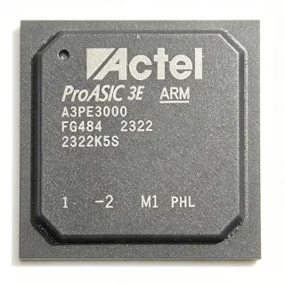
A3P600-1FGG484I - 600K Gate Flash FPGA 235 I/O | Microchip
Référence : A3P600-1FGG484I ✓ Actif| Qté | Prix unitaire | Total |
|---|---|---|
| 1 | $118.5 | $118,50 |
| 10 | $108.2 | $1 082,00 |
| 100 | $96.4 | $9 640,00 |
| 500 | $87.9 | $43 950,00 |
| 1 000 | $79.6 | $79 600,00 |
A3P600-1FGG484I Présentation
A flash-based FPGA is a type of field-programmable gate array that stores its configuration in on-chip flash memory cells rather than SRAM backed by an external configuration device. Within the programmable logic hierarchy, the A3P600 sits at the mid-density tier of the ProASIC3 family between the A3P400 and A3P1000, and as a nonvolatile device it belongs to the broader class of single-chip, live-reprogrammable power management... correction: programmable logic devices that boot instantly at power-up without a bootloader or external configuration flash.
Key features include single-chip nonvolatile operation that eliminates the external configuration PROM required by SRAM FPGAs, a 1.5V core voltage fabricated on a 130nm flash process, support for performance up to approximately 231 MHz system speed on this speed grade, and four I/O banks with independently supplyable VCCIB rails so mixed-voltage I/O standards can coexist on one device.
Technically, ProASIC3 uses the VersaTile architecture, in which every tile can act as a three-input lookup table, a D-flip-flop, or latching element, and the fabric is configured by charge-trapping flash cells. This yields instant-on behavior, low static power, and inherent security because the bitstream is never exposed on an external bus.
Typical applications include industrial automation control, military and aerospace subsystems, medical instrumentation, and communications bridge logic where instant power-up and configuration security matter.
Design consideration: only I/Os with compatible voltage standards should be assigned to the same VCCIB bank, per the Microchip I/O bank rules.
This page synthesizes distributor pricing, same-brand drop-in variants, and practical design notes not found in the manufacturer datasheet.
Alternatives de remplacement direct pour A3P600-1FGG484I — même boîtier, compatible broche à broche. Les références à boîtier différent nécessitant une retouche du PCB sont exclues.
Variantes de cette série
Modèles de la même série directement compatibles avec A3P600-1FGG484I (même facteur de forme et même empreinte) — différant par Package, Operating Temperature, Configuration Memory, Core Supply Voltage, Family.
Outil de comparaison rapide — sélectionnez des références alternatives pour une comparaison côte à côte :
A3P600-1FGG484
✅ Remplacement direct✓ En stock
$52.4 / unité
Voir la fiche technique →A3P600-FGG484I
✅ Remplacement direct✓ En stock
$55.3 / unité
Voir la fiche technique →A3P600-2FGG484I
✅ Remplacement direct✓ En stock
$31.8 / unité
Voir la fiche technique →A3P600L-1FGG484I
✅ Remplacement direct✓ En stock
$17.1 / unité
Voir la fiche technique →A3P600L-FGG484I
✅ Remplacement direct✓ En stock
$41.35 / unité
Voir la fiche technique →A3P600L-1FG484I
✅ Remplacement direct✓ En stock
Contactez-nous pour le prix
Voir la fiche technique →A3P600-FG484I
✅ Remplacement direct✓ En stock
$25.4 / unité
Voir la fiche technique →A3P600-1FGG484I Valeurs maximales et caractéristiques électriques
| Family | ProASIC3 |
| System Gates | 600000 |
| VersaTiles (D-flip-flops) | 13824 |
| User I/Os | 235 |
| Boîtier | 484-ball FBGA (FGG484) |
| Speed Grade | -1 |
| Core Voltage | 1.5 V |
| Technology | 130 nm flash process |
| Logic Architecture | VersaTile (LUT / D-flip-flop / latch) |
| Configuration Memory | On-chip flash (nonvolatile, single chip) |
| System Performance | Up to approx. 231 MHz (per Utmel family comparison) |
| I/O Banks | 4 (A3P600 per Microchip migration note) |
| Température de fonctionnement | Industrial (-40C to +100C), I suffix |
| Type de montage | Surface Mount |
| Reprogrammability | Live reprogrammable (in-system) |
Guide de configuration des broches du A3P600-1FGG484I 484-ball fbga (fgg484)
Configuration des broches du A3P600-1FGG484I (boîtier 484-ball fbga (fgg484)). Ce circuit intégré numérique comprend des GPIO, des interfaces de communication (UART, SPI, I2C) et des broches d'alimentation. Consultez la fiche technique du fabricant pour les fonctions alternatives des broches et les options de configuration. Indispensable pour la conception de systèmes embarqués et la conception de circuits imprimés.

Aucune donnée de brochage détaillée disponible pour A3P600-1FGG484I.
Consultez la fiche technique pour la configuration complète des broches.
Applications typiques
A3P600-1FGG484I convient pour 6 applications: Industrial Automation Control, Military and Aerospace Subsystems, Medical Instrumentation, Communications Bridge Logic, Secure Embedded Control, Test and Measurement Equipment.
Industrial Automation Control
The A3P600-1FGG484I fits industrial automation control because its 600k system gates and 235 user I/Os provide enough logic and connectivity for PLC I/O scanning, motor interface bridging, and sensor aggregation in one device. The industrial temperature rating of -40C to +100C covers factory-floor and outdoor cabinet environments, while instant-on flash configuration means the controller is live the moment power is applied, eliminating configuration boot delay that SRAM FPGAs introduce. The four independent VCCIB banks allow 3.3V, 2.5V, and 1.8V I/O standards to coexist, simplifying interfacing with legacy 5V-tolerant-adjacent logic families and modern low-voltage peripherals. Placed as the deterministic glue between a host CPU and field I/O, the A3P600-1FGG484I adds no operating-system jitter and its approximately 231 MHz system performance headroom covers most sequencing and protocol-bridging tasks.
Recommandé
Military and Aerospace Subsystems
Military and aerospace subsystems benefit from the A3P600-1FGG484I's on-chip flash configuration, which keeps the bitstream off the external bus and inherently resistant to readback attacks, a key reason ProASIC3 parts are positioned for defense applications by Microchip. The industrial -40C to +100C rating supports uncooled avionics bays and ground systems, and instant power-up matters in missions with strict time-to-ready requirements. With 600k gates and 13,824 VersaTiles, the device implements interface protocols, bus bridging, and signal preprocessing, while 235 user I/Os connect to mixed-voltage backplanes through four independent VCCIB banks. The flash fabric also shows deterministic single-event behavior relative to SRAM alternatives in many low-earth-orbit scenarios, though mission-specific radiation assessment remains the designer's responsibility per Microchip application guidance.
Recommandé
Medical Instrumentation
Medical instrumentation such as patient monitors, diagnostic analyzers, and imaging front ends uses the A3P600-1FGG484I as deterministic control and data-path logic. The instant-on flash configuration ensures the instrument is operational immediately at power-up, important for devices with rapid startup expectations and for safety logic that must be active before a host processor boots. Its 235 user I/Os handle sensor arrays, touch panels, and communication interfaces, and the four independently supplied I/O banks allow clean separation of noisy digital domains from sensitive analog-adjacent control signals. Because the configuration is nonvolatile and secure on-chip, patient-data-handling hardware benefits from reduced bitstream exposure. The -1 speed grade at up to approximately 231 MHz comfortably covers typical acquisition sequencing and preprocessing rates while keeping power and cost below faster-binned equivalents.
Recommandé
Communications Bridge Logic
In communications equipment, the A3P600-1FGG484I serves as bridge and glue logic between line cards, backplanes, and management controllers. The 600k-gate fabric implements multiple protocol interfaces concurrently, and approximately 231 MHz of system performance covers common link-layer tasks on the -1 speed grade. The four VCCIB banks let designers mix 3.3V legacy PHY interfaces with 1.8V or 2.5V modern serial-adjacent control signals on one chip, eliminating level-shifters and their latency. Instant-on flash configuration means links initialize without waiting for a bitstream load from external memory, reducing link-recovery time after power events, which matters in carrier infrastructure availability targets. The 484-ball FGG484 package provides the 235 usable I/Os needed for wide parallel buses and dense control planes in rack-mounted equipment.
Recommandé
Secure Embedded Control
Secure embedded control systems, including encryption-key holders, anti-tamper controllers, and secure boot companions, exploit the A3P600-1FGG484I's on-chip flash configuration. Unlike SRAM FPGAs that expose the configuration bitstream on an external bus at every power-up, the ProASIC3 fabric is programmed through charge-trapping flash cells on the die itself, dramatically reducing interception opportunities. The device operates instantly, so secure state machines enforcing power-good and tamper-detect sequencing can be active before other system elements come alive. With 600k gates, designers can implement symmetric ciphers, hash functions, and stateful monitors alongside control logic, and 235 I/Os connect sensors, switches, and alert paths across four voltage banks. Per Microchip product positioning, low total cost of ownership and single-chip operation further reduce the physical attack surface of the bill of materials.
Recommandé
Test and Measurement Equipment
Bench and modular test instruments use the A3P600-1FGG484I for timing generation, trigger routing, and interface adaptation. The 13,824 VersaTiles implement counters, delay lines, and pattern generators deterministically, and the -1 speed grade supports trigger pipelines well within its approximately 231 MHz fabric capability. The industrial -40C to +100C rating covers uncalibrated storage and transport conditions, while instant-on configuration ensures the instrument front end is controllable the moment power is applied, simplifying self-test sequencing. The 235 user I/Os fan out to relay banks, ADC control buses, and host interfaces (USB, LAN module bridges), and four independent VCCIB banks isolate noisy switching domains from precision timing I/O. Compared with an SRAM FPGA plus configuration flash, the single-chip flash solution reduces the instrument BOM and removes a field-update failure mode tied to external config memory corruption.
Recommandé
Récapitulatif des produits recommandés
Données de référence d'ingénierie pour A3P600-1FGG484I — comparaison, recommandations de conception et informations de conformité.
Guide de sélection
Comparaison avec les alternatives
| Paramètre | Ce produit | A3P600-1FGG484 | A3P600-FGG484I | A3P600-2FGG484I | A3P600L-1FGG484I |
|---|---|---|---|---|---|
| Package | 484-ball FBGA (FGG484) | 484-ball FBGA (FGG484) - same | 484-ball FBGA (FGG484) - same | 484-ball FBGA (FGG484) - same | 484-ball FBGA (FGG484) - same |
| Brand | Microchip Technology | Microchip Technology | Microchip Technology | Microchip Technology | Microchip Technology |
| System Gates | 600000 | 600000 | 600000 | 600000 | 600000 |
| User I/Os | 235 | 235 | 235 | 235 | 235 |
| Speed Grade | -1 | -1 | Standard | -2 (faster) | -1 |
| Temperature Range | Industrial (-40C to +100C) | Commercial | Industrial (-40C to +100C) | Industrial (-40C to +100C) | Industrial (-40C to +100C) |
| Configuration Memory | On-chip flash (nonvolatile) | On-chip flash (nonvolatile) | On-chip flash (nonvolatile) | On-chip flash (nonvolatile) | On-chip flash (nonvolatile) |
| Core Voltage | 1.5 V | 1.5 V | 1.5 V | 1.5 V | 1.5 V (low-power process) |
Principaux différenciateurs
- Instant-on single-chip nonvolatile configuration (vs A2F500M3G-1FGG484I (SmartFusion))
- Cost-optimized -1 speed grade (vs A3P600-2FGG484I)
- Industrial temperature qualification (vs A3P600-1FGG484)
- Trade-off: higher static power than low-power variant (vs A3P600L-1FGG484I)
Notes de conception
The A3P600-1FGG484I requires a 1.5V core supply plus separate VCCIBx supplies for each of its four I/O banks. Estimated: total power is dominated by dynamic switching and I/O loading; use Microchip's ProASIC3 power calculator in Libero SoC with your actual toggle rates rather than rule-of-thumb estimates. Sequence core and I/O rails per the datasheet power-up specification to avoid latch-up paths, and decouple each VCCIB bank locally with at least 10uF bulk plus 0.1uF ceramic capacitors placed at the bank supply balls.
Plan I/O bank assignment before routing: only I/Os with compatible voltage standards may share a VCCIB bank, per the Microchip migration application note which states 'package VCCIBx pins are routed through the corresponding banks of the devices' and that only compatible standards may be assigned to the same bank. Obtain the exact 484-ball ball map from the official Microchip ProASIC3 datasheet and lock your pin constraints in Libero SoC early, because changing a bank voltage after routing forces a PCB respin.
Estimated: a 484-ball FBGA with a 1.5V core dissipates modest heat at typical -1 speed-grade utilization; still, verify junction temperature using the theta-JA value from the datasheet package thermal table with your actual airflow. For conduction-cooled enclosures typical of defense builds, bond the board to a cold plate and confirm the die-junction-to-board resistance from the datasheet rather than assuming still-air values.
Do not substitute the commercial-temperature A3P600-1FGG484 into a design validated at -40C; only the I-suffix industrial parts cover the full industrial range. Conversely, upgrading from A3P600-1FGG484I to A3P600-2FGG484I improves timing margins but changes I/O timing parameters, so re-run I/O timing checks in Libero. Finally, the -1 part is carried by limited distribution (Octopart lists 1 distributor for this suffix), so secure production stock early.
Informations de conformité
Compliance status not stated in retrieved data. Microchip ProASIC3 parts are generally RoHS-compliant in current FGG (lead-free ball) suffixes, but verify on the official Microchip product page before relying on this. Note: FGG vs FG suffixes may indicate lead-free (Green) packaging differences.