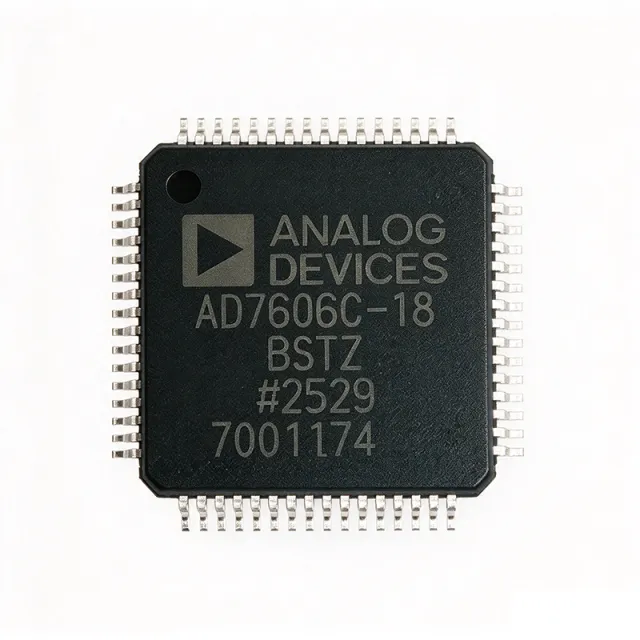
AD7606C-18BSTZ - 18-Bit 8-Ch 1MSPS DAS ADC | Analog Devices
料号: AD7606C-18BSTZ ✓ 量产中| 数量 | 单价 | 小计 |
|---|---|---|
| 1 | $49.2188 | $49.22 |
| 10 | $35.5469 | $355.47 |
| 100 | $31.4453 | $3,144.53 |
| 500 | $30.0781 | $15,039.05 |
| 1,000 | $28.7109 | $28,710.90 |
AD7606C-18BSTZ 概述
A simultaneous-sampling SAR ADC is a category of precision data converter that captures the instantaneous voltage on all input channels at the same instant under one common convert-start signal, then performs a binary-search quantization in successive bit decisions per channel. The AD7606C-18 sits inside the hierarchy: SAR ADC -> data acquisition system (DAS) -> precision ADC -> analog-to-digital converter -> mixed-signal IC. Synchronous multi-channel acquisition is essential when phase relationships between signals must be preserved.
Key features include an on-chip digital filter with oversampling ratios from 2x to 256x, integrated analog input clamps with ±16.5 V tolerance, a per-channel PGA with hardware gain settings of 1, 2, 4, 8, 16, 32, and 64, and both parallel and serial (SPI-/QSPI-/MICROWIRE-/DSP-compatible) host interfaces. Throughput remains 1 MSPS per channel across all eight channels simultaneously, with SNR of approximately 91 dB and THD near -100 dB at the maximum sampling rate. The 5 V single-supply operation simplifies system power design versus traditional ±15 V industrial front ends.
The architecture pairs a high-impedance input front end (typically 1 MΩ) with a charge-redistribution SAR core, controlled by an internal precision reference and a flexible sequencer. Hardware overrange detection and per-channel sequencer flags accelerate FPGA-/DSP-side post-processing. An extended operating temperature range of -40 °C to +85 °C supports industrial deployment, and the part is rated to withstand ±16.5 V analog overvoltages on every input without damage.
Typical applications include three-phase power-line monitoring and protection relays, multi-axis industrial motor control, patient monitoring ECG/EEG front ends, vibration and structural-health data loggers, and high-channel-count data acquisition modules. The combination of true bipolar inputs, simultaneous sampling, integrated analog front end, and on-chip reference makes the AD7606C-18 a single-chip replacement for legacy multi-component discrete DAS front ends.
When designing with the AD7606C-18, allocate the LQFP-64 land pattern with thermal copper pour tied to the exposed pad (EP) for lowest junction-to-ambient resistance, and use 100 nF plus 10 µF decoupling on AVDD/AVDD_DR with 100 nF plus 10 µF on VDRIVE close to the device. Drive CONVST with a clean low-jitter source; jitter couples directly to the SNR budget. For best DC accuracy, allow the on-chip reference a 5 ms settling after power-up.
This page synthesizes distributor stock and price tiers (DigiKey), verified drop-in alternatives, parametric comparison vs Analog Devices pin-compatible siblings, and practical PCB/thermal/decoupling notes not collated in the manufacturer datasheet alone.
直接替换替代料: AD7606C-18BSTZ ——相同封装,引脚兼容。需要 PCB 改动的不同封装料号已排除。
快速对比工具——选择替代料号进行并排对比:
AD7606C-16BSTZ
✓ 有现货
$49.2188 / 个
查看数据手册 →AD7606BSTZ
✓ 有现货
$16.9 / 个
查看数据手册 →AD7606BSTZ-4
✓ 有现货
$11.6 / 个
查看数据手册 →AD7606C-18BSTZ-RL
📋 参考替代料(不在目录中)
AD7607BSTZ
📋 参考替代料(不在目录中)
ADS8588S
📋 参考替代料(不在目录中)
AD7606C-18BSTZ 最大额定值与电气特性
| Number of Channels | 8 |
| 分辨率 | 18 bit |
| Architecture | SAR (Successive Approximation Register) |
| Sampling Rate (per channel) | 1 MSPS (all channels simultaneous) |
| Analog Input Range (True Bipolar) | ±10 V, ±5 V, 0 V to 10 V (software-selectable) |
| Analog Input Overvoltage Tolerance | ±16.5 V |
| Analog Supply Voltage (AVDD) | 4.75 V to 5.25 V (single 5 V supply) |
| Digital I/O Supply (VDRIVE) | 2.3 V to 5.25 V |
| Input Impedance | 1 MΩ typical |
| PGA Gain Settings | 1, 2, 4, 8, 16, 32, 64 (hardware-selectable) |
| On-chip Reference Voltage | 2.5 V low-drift precision |
| Oversampling (Digital Filter) Ratios | 2x, 4x, 8x, 16x, 32x, 64x, 128x, 256x |
| Host Interface | Parallel + Serial (SPI/QSPI/MICROWIRE/DSP-compatible) |
| SNR (typ, 1 MSPS, ±10 V) | 91 dB |
| THD (typ) | -100 dB |
| 工作温度 | -40 °C to +85 °C |
| 封装 | 64-LQFP (10 mm x 10 mm) |
| 安装类型 | Surface Mount |
| MSL 等级 | 3 |
| RoHS 状态 | Compliant |
AD7606C-18BSTZ 引脚配置
| 引脚 1 | DGND — Digital ground |
| 引脚 2 | VDRIVE — Logic interface supply (2.3 V - 5.25 V) |
| 引脚 3 | CONVST_A — Conversion start, analog inputs V1-V4 |
| 引脚 4 | CONVST_B — Conversion start, analog inputs V5-V8 |
| 引脚 5 | RD/SCLK — Read strobe (parallel) or serial clock (serial mode) |
| 引脚 6 | CS — Chip select, active low |
| 引脚 7 | RESET — Hardware reset, active low |
| 引脚 8 | OS0 — Oversampling ratio select bit 0 |
| 引脚 9 | OS1 — Oversampling ratio select bit 1 |
| 引脚 10 | OS2 — Oversampling ratio select bit 2 |
| 引脚 11 | RANGE — Analog input range select (0 = ±10 V, 1 = ±5 V/0-10 V) |
| 引脚 12 | AVDD — 5 V analog supply |
| 引脚 13 | AGND — Analog ground |
| 引脚 14 | V1 — Analog input channel 1 |
| 引脚 15 | V1_GND — Channel 1 ground reference |
| 引脚 16 | V2 — Analog input channel 2 |
| 引脚 17 | V2_GND — Channel 2 ground reference |
| 引脚 18 | V3 — Analog input channel 3 |
| 引脚 19 | V3_GND — Channel 3 ground reference |
| 引脚 20 | V4 — Analog input channel 4 |
| 引脚 21 | V4_GND — Channel 4 ground reference |
| 引脚 22 | REF — Reference decoupling / external reference input (2.5 V) |
| 引脚 23 | REGCAPA — Internal LDO output, decouple with 1 µF |
| 引脚 24 | REGCAPB — Internal LDO output, decouple with 1 µF |
| 引脚 25 | AGND — Analog ground |
| 引脚 26 | AVDD — 5 V analog supply |
| 引脚 27 | V5 — Analog input channel 5 |
| 引脚 28 | V5_GND — Channel 5 ground reference |
| 引脚 29 | V6 — Analog input channel 6 |
| 引脚 30 | V6_GND — Channel 6 ground reference |
| 引脚 31 | V7 — Analog input channel 7 |
| 引脚 32 | V7_GND — Channel 7 ground reference |
| 引脚 33 | V8 — Analog input channel 8 |
| 引脚 34 | V8_GND — Channel 8 ground reference |
| 引脚 35 | REFGND — Reference ground |
| 引脚 36 | AVDD_DR — 5 V supply for input driver section |
| 引脚 37 | AGND — Analog ground |
| 引脚 38 | DB0 — Parallel data output bit 0 / DOUT serial |
| 引脚 39 | DB1 — Parallel data output bit 1 |
| 引脚 40 | DB2 — Parallel data output bit 2 |
| 引脚 41 | DB3 — Parallel data output bit 3 |
| 引脚 42 | DB4 — Parallel data output bit 4 |
| 引脚 43 | DB5 — Parallel data output bit 5 |
| 引脚 44 | DB6 — Parallel data output bit 6 |
| 引脚 45 | DB7 — Parallel data output bit 7 |
| 引脚 46 | DGND — Digital ground |
| 引脚 47 | DB8 — Parallel data output bit 8 |
| 引脚 48 | DB9 — Parallel data output bit 9 |
| 引脚 49 | DB10 — Parallel data output bit 10 |
| 引脚 50 | DB11 — Parallel data output bit 11 |
| 引脚 51 | DB12 — Parallel data output bit 12 |
| 引脚 52 | DB13 — Parallel data output bit 13 |
| 引脚 53 | DB14 — Parallel data output bit 14 |
| 引脚 54 | DB15/BUSY — Parallel data bit 15 (parallel mode) / BUSY output (serial mode) |
| 引脚 55 | FRSTDATA — First data indicator in serial mode |
| 引脚 56 | STBY — Standby mode, active low |
| 引脚 57 | DGND — Digital ground |
| 引脚 58 | VDRIVE — Logic interface supply |
| 引脚 59 | DB16 — Parallel data output bit 16 (extended mode) |
| 引脚 60 | DB17 — Parallel data output bit 17 (extended mode) |
| 引脚 61 | NC — Not connected (per datasheet) |
| 引脚 62 | NC — Not connected (per datasheet) |
| 引脚 63 | EP — Exposed pad (must be soldered to AGND thermal plane) |
| 引脚 64 | AGND — Analog ground |
典型应用
AD7606C-18BSTZ 适用于 6 应用s: Three-Phase Power-Line Monitoring Relays, Multi-Axis Industrial Motor Control, Patient Monitoring - ECG / EEG Front End, Vibration and Structural-Health Data Loggers, High-Channel-Count Data Acquisition Modules, Power Quality and Harmonic Analyzers.
Three-Phase Power-Line Monitoring Relays
The AD7606C-18BSTZ is purpose-built for three-phase power-line monitoring and protection relays. Simultaneous sampling of all eight channels preserves the exact phase relationship between phase-A/B/C voltage and current waveforms, which is critical for accurate real/reactive/apparent power calculation and for harmonic analysis to IEC 61000-4-7. The ±10 V true bipolar input range directly accepts PT/CT secondary outputs without external signal conditioning, and the integrated 91 dB SNR delivers class-0.2/0.5 revenue-grade metering accuracy. The on-chip 2.5 V reference and reference buffer eliminate the need for a discrete ADR45xx reference, reducing BOM cost and PCB area in substation-grade relay designs.
推荐
Multi-Axis Industrial Motor Control
In multi-axis servo drives and industrial motor controllers, the AD7606C-18BSTZ simultaneously samples eight channels of phase current, bus voltage, and resolver feedback at 1 MSPS per channel, providing the deterministic latency required for field-oriented control (FOC) loops running at 20-50 kHz. The integrated PGA with gains up to 64 allows direct connection to low-amplitude shunt signals without external instrumentation amplifiers, while the on-chip digital filter with up to 256x oversampling improves effective resolution by ~5 dB for low-bandwidth vibration monitoring. The 5 V single-supply operation and integrated analog input clamps to ±16.5 V protect the ADC from inverter switching transients in 600 V class drives.
推荐
Patient Monitoring - ECG / EEG Front End
Medical patient monitors for ECG, EEG, and EMG signal acquisition benefit from the AD7606C-18BSTZ's 18-bit resolution and 91 dB SNR, which exceed IEC 60601-2-25/-2-47 diagnostic ECG requirements by 10+ dB. The ±10 V bipolar input range accepts the amplified output of standard instrumentation-amp front ends (e.g., AD8232, ADAS1000) without additional scaling. Eight simultaneously-sampled channels enable capture of 12-lead ECG plus four auxiliary channels (respiration, SpO2, temperature) in a single IC, reducing the bill of materials versus multi-chip architectures. The 64-LQFP package's 10x10 mm footprint fits comfortably inside portable patient monitor enclosures.
推荐
Vibration and Structural-Health Data Loggers
The AD7606C-18BSTZ's 18-bit resolution and 1 MSPS simultaneous sampling on all eight channels make it ideal for multi-axis vibration, modal analysis, and structural-health monitoring (SHM) data loggers used in aerospace, civil engineering, and predictive maintenance applications. The on-chip oversampling digital filter (up to 256x) extends dynamic range to ~21 effective bits at lower throughput, capturing both high-frequency rotor harmonics and low-amplitude bearing-fault signatures from IEPE accelerometers. Simultaneous sampling eliminates inter-channel phase error that would corrupt transfer-function measurements in modal hammer tests.
推荐
High-Channel-Count Data Acquisition Modules
Modular PXI/PCIe/LXI data acquisition cards and modular instrumentation use the AD7606C-18BSTZ to deliver 8 channels of true bipolar ±10 V input at 1 MSPS/ch from a single 64-LQFP IC. Per-channel hardware gain settings of 1/2/4/8/16/32/64 plus on-chip input clamps eliminate the need for external instrumentation amps and protection relays in front-end daughter cards, allowing up to 64 channels per PXI slot through daisy-chained serial interfaces. The parallel interface option delivers full 1 MSPS throughput for transient capture, while the SPI mode simplifies routing on high-density cards.
推荐
Power Quality and Harmonic Analyzers
The AD7606C-18BSTZ's 91 dB SNR, -100 dB THD, and simultaneous eight-channel sampling make it suitable for class-A power quality analyzers and IEC 61000-4-30-compliant harmonic measurement instruments. The on-chip digital filter provides windowed anti-alias filtering at fixed decimation ratios, simplifying EN 50160 / IEEE 519 compliance verification. With eight channels one IC can simultaneously monitor three phase voltages, three phase currents, neutral current, and DC bus voltage at 1 MSPS/ch, capturing transient events with sub-microsecond time alignment across all measurements.
推荐
推荐产品汇总
工程参考数据: AD7606C-18BSTZ ——对比、设计指导和合规信息。
选型指南
与替代料对比
| 参数 | 本产品 | AD7606C-16BSTZ | AD7606C-18BSTZ-RL | AD7606BSTZ | AD7606BSTZ-4 | AD7607BSTZ | ADS8588S |
|---|---|---|---|---|---|---|---|
| Brand | Analog Devices | Analog Devices | Analog Devices | Analog Devices | Analog Devices | Analog Devices | Texas Instruments |
| Package | 64-LQFP (10x10) | 64-LQFP (10x10) - same | 64-LQFP (10x10) - same | 64-LQFP (10x10) - same | 64-LQFP (10x10) - same | 64-LQFP (10x10) - same | LQFP-64 (10x10) - same footprint family |
| Resolution | 18 bit | 16 bit | 18 bit (same die) | 16 bit | 16 bit | 14 bit | 16 bit |
| Channels | 8 | 8 | 8 | 8 | 8 | 8 | 8 |
| Sampling Rate (per channel) | 1 MSPS | 1 MSPS | 1 MSPS | 200 kSPS | 200 kSPS | 200 kSPS | 200 kSPS |
| Input Range | ±10 V / ±5 V / 0-10 V | ±10 V / ±5 V / 0-10 V | ±10 V / ±5 V / 0-10 V | ±10 V / ±5 V / 0-10 V | ±5 V only | ±10 V / ±5 V / 0-10 V | ±10 V / ±5 V |
| On-chip Digital Filter / OSR | Yes, up to 256x | Yes, up to 256x | Yes, up to 256x | No oversampling | No oversampling | No oversampling | No on-chip filter |
| PGA Gain | 1, 2, 4, 8, 16, 32, 64 | 1, 2, 4, 8, 16, 32, 64 | 1, 2, 4, 8, 16, 32, 64 | No PGA | No PGA | No PGA | No PGA |
| Analog Supply | Single 5 V | Single 5 V | Single 5 V | Single 5 V | Single 5 V | Single 5 V | Single 5 V |
| Unit Price (qty 1, USD, as of 2026-10-06) | 38.50 | approximately 32.00 | approximately 38.50 (reel) | approximately 14.00 | approximately 15.00 | approximately 11.00 | approximately 13.50 |
关键差异点
- 18-bit resolution vs 16-bit in same package (对比 AD7606C-16BSTZ)
- 5x higher throughput than legacy AD7606 family (对比 AD7606BSTZ)
- Integrated PGA and digital oversampling filter (对比 AD7606BSTZ-4)
设计说明
Decouple each AVDD and AVDD_DR pin with a 100 nF X7R ceramic placed within 2 mm of the pin, plus a shared 10 µF X5R bulk capacitor on each rail. VDRIVE (logic I/O supply) requires its own 100 nF + 10 µF pair even if VDRIVE = 5 V. Tie REGCAPA and REGCAPB each to AGND through a 1 µF X7R capacitor - these are the internal LDO outputs and must be stable. Source: AD7606C-18 datasheet power-supply section.
Solder the exposed pad (EP) of the 64-LQFP directly to a continuous AGND copper pour on the top layer (minimum 1 sq inch, 2 oz copper preferred). The EP is the primary thermal path; without it junction-to-ambient thermal resistance rises above 60 C/W and may trigger thermal shutdown at sustained 1 MSPS operation with all channels active. Source: AD7606C-18 datasheet package thermal characteristics.
Route each analog input (V1-V8) with a tightly-coupled dedicated ground return (Vx_GND) - do not share analog grounds between channels. Use a star-ground topology where Vx_GND pins tie to a single AGND plane near the ADC. Keep digital lines (CONVST, RD, DB0-DB17) on the opposite side of the PCB from analog inputs to minimize digital coupling into the high-impedance 1 MΩ analog front end. Source: AD7606C-18 datasheet layout guidelines.
Drive CONVST_A/CONVST_B with a low-jitter (<50 ps RMS) source. Aperture jitter appears directly in the SNR budget: at 1 MSPS with 18-bit target, total jitter must remain below 0.5 ns RMS. Many MCUs' GPIO toggles exceed this - use an FPGA or a dedicated clock generator. Also, allow 5 ms after power-up for the internal 2.5 V reference to settle before initiating conversions; reading immediately produces 2-3 LSB gain error. Source: AD7606C-18 datasheet timing and reference settling.
Estimated: at the maximum 18-bit ENOB target (~91 dB SNR), the input source impedance seen by V1-V8 should remain below 1 kΩ to avoid THD degradation from the 1 MΩ/8 pF input stage. For source impedances above 5 kΩ add a 1 nF C0G bypass directly at each Vx pin to preserve settling. Overrange detection on each channel should be monitored by the host to flag clipped samples during transient capture. Source: AD7606C-18 datasheet analog input section.
合规信息
RoHS and REACH compliance per Analog Devices product page. Not AEC-Q100 qualified - this part targets industrial instrumentation, not automotive. Lead-free (Pb-free) reflow profile per JEDEC J-STD-020 MSL3.







