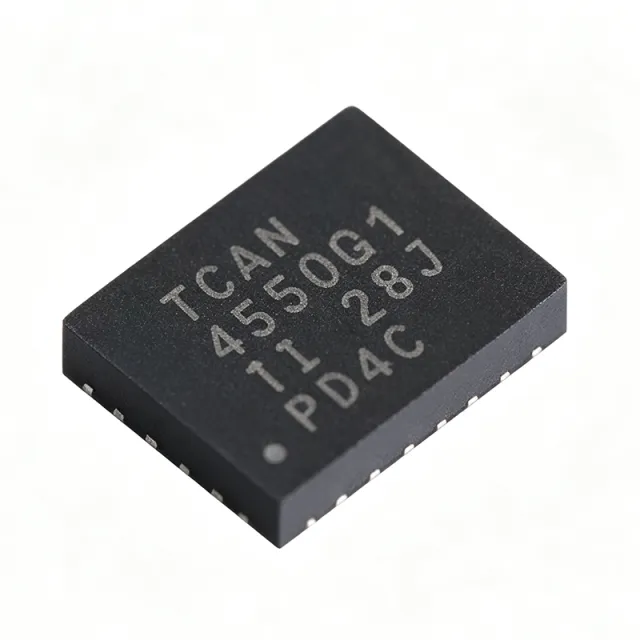
TCAN4550RGYRQ1 - CAN FD SBC with Transceiver 8Mbps VQFN-20 | TI
料号: TCAN4550RGYRQ1 ✓ 量产中| 数量 | 单价 | 小计 |
|---|---|---|
| 1 | $5.2 | $5.20 |
| 10 | $4.68 | $46.80 |
| 100 | $4.15 | $415.00 |
| 500 | $3.55 | $1,775.00 |
| 1,000 | $3.1 | $3,100.00 |
TCAN4550RGYRQ1 概述
A CAN FD (Controller Area Network Flexible Data Rate) system basis chip is an integrated mixed-signal IC that combines the ISO 11898-1 data link layer controller, the ISO 11898-2 physical layer transceiver, and an internal logic LDO into a single package. The CAN FD protocol extends classic CAN by allowing a higher data payload and a flexible bit rate, enabling automotive networks to scale from 1 Mbps to 8 Mbps while preserving the deterministic arbitration of classic CAN. Integrating the controller and the transceiver on one die reduces PCB area, removes the high-speed digital signals between two separate ICs, and improves EMC robustness versus discrete controller-plus-transceiver implementations.
Key specifications of the TCAN4550RGYRQ1 include CAN FD data rates up to 8 Mbps, ISO 11898-2:2016 physical layer compliance, an SPI host interface up to 10 MHz, integrated 5V/3.3V selectable LDO for VCC logic supply, low-power standby and sleep modes, and a watchdog timer. The 20-pin VQFN package with exposed thermal pad supports automotive power profiles while staying within a 3.5 x 4.5 mm footprint suitable for space-constrained ECUs.
The TCAN4550-Q1 uses a high-speed CAN transceiver with explicit bus-fault protection, thermal shutdown, and wide common-mode range for reliable communication on 12V automotive bus networks. The on-chip LDO generates the logic supply from the 5V CAN rail, removing the need for an external regulator in many applications. SPI registers expose CAN ID filters, bit-timing parameters (sample point and propagation delay), and diagnostic counters, which simplifies firmware bring-up.
Typical applications include automotive body control modules, gateways, battery management systems (BMS), powertrain ECUs, ADAS sensor nodes, and industrial CAN FD networks. The 8 Mbps capability is particularly valuable for high-throughput diagnostics and emerging zonal architectures in modern vehicles.
Designers should connect the exposed pad to a solid ground plane for thermal dissipation, place 100 nF + 1uF decoupling close to VCC and VIO pins, and follow ISO 11898-2 bus-termination guidance (60 ohm / 120 ohm) on the CANH/CANL differential pair. Verify SPI mode 0 timing against microcontroller datasheet before enabling CAN bus activity. This page synthesizes distributor pricing, drop-in alternatives, and design considerations not consolidated in the manufacturer datasheet.
直接替换替代料: TCAN4550RGYRQ1 ——相同封装,引脚兼容。需要 PCB 改动的不同封装料号已排除。
本系列中的变体
可与以下型号直接替换的同系列型号: TCAN4550RGYRQ1 (相同外形与封装尺寸) ——差异在于 Package, Protocol, Number of Drivers/Receivers, RoHS Status, Automotive Qualification.
快速对比工具——选择替代料号进行并排对比:
TCAN4550RGYR
✅ 直接替换📋 参考替代料(不在目录中)
TCAN4550RGYTQ1
✅ 直接替换📋 参考替代料(不在目录中)
TCAN1044DRQ1
✅ 直接替换 ⚠️ 规格未核验✓ 有现货
$0.62 / 个
查看数据手册 →TCAN1051-Q1
✅ 直接替换✓ 有现货
$1.05 / 个
查看数据手册 →TCAN1051DRBRQ1
✅ 直接替换✓ 有现货
$1.18 / 个
查看数据手册 →TCAN4550RGYRQ1 最大额定值与电气特性
| Product Type | Automotive System Basis Chip (SBC) with CAN FD Controller and Transceiver |
| Data Protocol | CAN FD (ISO 11898-1:2015) / CAN 2.0B |
| Physical Layer Compliance | ISO 11898-2:2016 high-speed CAN |
| Maximum Data Rate | 8 Mbps |
| Logic Supply (VIO) | 1.8V / 3.3V / 5V selectable |
| Host Interface | SPI up to 10 MHz, mode 0/1 |
| Integrated LDO | Yes (5V or 3.3V selectable output) |
| Low-Power Modes | Standby and Sleep |
| Watchdog Timer | Yes (SPI-driven window watchdog) |
| 工作温度 | -40C to +125C |
| 封装 | 20-pin VQFN (RGY) 3.5 x 4.5 mm with exposed pad |
| Automotive Qualification | AEC-Q100 Grade 1 |
| 安装类型 | Surface Mount |
| RoHS 状态 | Compliant |
| Number of Channels | 1 CAN FD channel |
| Common-Mode Range | -12V to +12V (CAN bus) |
TCAN4550RGYRQ1 引脚配置
| 引脚 1 | VBAT — Battery / supply voltage input (typically 5V-18V from automotive bus) |
| 引脚 2 | VCC — 5V regulator output / CAN transceiver supply |
| 引脚 3 | GND — Ground |
| 引脚 4 | CANH — CAN high-side differential bus line |
| 引脚 5 | CANL — CAN low-side differential bus line |
| 引脚 6 | INH — Inhibit / wake output (high when active) |
| 引脚 7 | WAKE — Wake-up input from bus |
| 引脚 8 | RSTn — Reset input (active low) |
| 引脚 9 | CSn — SPI chip select (active low) |
| 引脚 10 | SCLK — SPI clock input |
| 引脚 11 | SDI — SPI data in (MOSI) |
| 引脚 12 | SDO — SPI data out (MISO) |
| 引脚 13 | INTn — Interrupt output to MCU (active low) |
| 引脚 14 | GPIO1 — General purpose IO / wake source |
| 引脚 15 | GPIO2 — General purpose IO |
| 引脚 16 | VIO — Host-side logic supply (1.8V / 3.3V / 5V) |
| 引脚 17 | VDD — Internal digital core supply |
| 引脚 18 | NC — Not connected (per datasheet) |
| 引脚 19 | NC — Not connected (per datasheet) |
| 引脚 20 | NC — Not connected (per datasheet) |
| 引脚 EP | GND Pad — Exposed thermal pad - must be soldered to ground plane |
典型应用
TCAN4550RGYRQ1 适用于 7 应用s: Automotive Body Control Module (BCM), Automotive Gateway ECU, Battery Management System (BMS) for EV, ADAS Sensor Nodes (Radar/Lidar), Industrial CAN FD Networks (Modbus/IoT), Powertrain / Engine Control ECU, Charger and DC-DC Converter Modules.
Automotive Body Control Module (BCM)
The TCAN4550RGYRQ1's 8 Mbps CAN FD support, -40C to +125C operation, and AEC-Q100 qualification make it a strong fit for body control modules driving lighting, seat, mirror, and door-zone ECUs. Compared to classic CAN at 1 Mbps, FD tripling the payload reduces bus load by 60% on multi-zone BCMs. The SPI host interface streams 50+ messages per second to the body MCU without burdening the SPI bus. The integrated LDO removes the external 3.3V regulator that discrete transceiver stacks typically require for the host-side logic rail, saving BOM and PCB area.
推荐
Automotive Gateway ECU
In zonal or central gateway ECUs, the TCAN4550RGYRQ1's 8 Mbps capability lets it aggregate 4-8 CAN FD channels from sub-networks and forward high-throughput diagnostic traffic to the central compute. The integrated LDO and watchdog timer reduce external component count in the gateway, which typically hosts 4-12 SBCs. AEC-Q100 Grade 1 supports underhood gateway placement where ambient temperatures exceed 85C. Use multiple TCAN4550RGYRQ1 devices in parallel for redundant gateways with deterministic SPI control.
推荐
Battery Management System (BMS) for EV
The TCAN4550RGYRQ1 serves BMS master and cell-monitoring modules in 400V and 800V EV battery packs, where CAN FD's 8 Mbps accelerates cell-balancing data upload to the pack controller. The integrated transceiver's -12V to +12V common-mode range survives ground-shift transients from 200A+ battery currents during pre-charge. AEC-Q100 Grade 1 tolerates underpack temperatures of 105C. The integrated 5V LDO can power external cell-monitor ICs, eliminating one regulator in the BOM.
推荐
ADAS Sensor Nodes (Radar/Lidar)
ADAS radar and lidar ECUs use the TCAN4550RGYRQ1's 8 Mbps CAN FD to push high-bandwidth object-list data upstream to the fusion ECU in real time. The SPI host interface lets the radar MCU run free of CAN interrupt overhead. AEC-Q100 Grade 1 handles thermal load in windshield-mounted or bumper-mounted sensor pods. Integrated LDO simplifies the power tree where PCB area is constrained to 25 x 35 mm.
推荐
Industrial CAN FD Networks (Modbus/IoT)
Industrial CANopen and CANopen FD nodes use the TCAN4550RGYRQ1 (or the non-automotive TCAN4550RGYR variant) for PLC-to-remote-IO communication. The 8 Mbps CAN FD dramatically reduces scan time on multi-axis motion-control networks versus classic CAN at 1 Mbps. The integrated LDO handles 24V industrial input via an upstream switching regulator. The SPI host interface allows simple microcontroller arbitration across multi-vendor industrial networks.
推荐
Powertrain / Engine Control ECU
Powertrain ECUs leverage the TCAN4550RGYRQ1's 8 Mbps CAN FD for diagnostics, calibration, and OBD-III communications on gasoline and diesel platforms. The AEC-Q100 Grade 1 (-40C to +125C) rating sustains underhood ambient at 110C+ with engine-on duty cycles. The integrated LDO simplifies harsh-environment power design. Lower bit-rate operation (500 kbps) remains supported, so existing classic-CAN calibration tools do not require firmware updates.
推荐
Charger and DC-DC Converter Modules
Onboard EV chargers and DC-DC converters use the TCAN4550RGYRQ1 to communicate charging status, fault flags, and high-voltage telemetry over CAN FD to the vehicle master. The integrated LDO removes an external regulator in the high-voltage isolation boundary. The exposed pad of the 20-pin VQFN package supports sustained operation at 1W bus-load in the charger enclosure. The wide common-mode range tolerates chassis-ground shift on 800V architectures.
推荐
推荐产品汇总
工程参考数据: TCAN4550RGYRQ1 ——对比、设计指导和合规信息。
选型指南
与替代料对比
| 参数 | 本产品 | TCAN4550RGYR | TCAN4550RGYTQ1 | TCAN1044DRQ1 | TCAN1051-Q1 | TCAN1051DRBRQ1 |
|---|---|---|---|---|---|---|
| Brand | Texas Instruments | Texas Instruments | Texas Instruments | Texas Instruments | Texas Instruments | Texas Instruments |
| Package | VQFN-20 (RGY) 3.5x4.5 mm | VQFN-20 (RGY) - same | VQFN-20 (RGY) - same | VQFN-20 family | VQFN-20 family | VQFN-20 family |
| Function | Controller + Transceiver + LDO (SBC) | Controller + Transceiver + LDO (SBC) | Controller + Transceiver + LDO (SBC) | Transceiver only | Transceiver only | Transceiver only |
| CAN FD Data Rate | 8 Mbps | 8 Mbps | 8 Mbps | 8 Mbps | 5 Mbps | 5 Mbps |
| AEC-Q100 | Grade 1 | Not qualified (industrial) | Grade 1 | Grade 1 | Grade 1 | Grade 1 |
| Integrated LDO | Yes (5V/3.3V selectable) | Yes (5V/3.3V selectable) | Yes (5V/3.3V selectable) | No (transceiver only) | No (transceiver only) | No (transceiver only) |
| Host Interface | SPI (up to 10 MHz) | SPI (up to 10 MHz) | SPI (up to 10 MHz) | N/A (transceiver) | N/A (transceiver) | N/A (transceiver) |
| Operating Temperature | -40C to +125C | -40C to +125C | -40C to +125C | -40C to +150C | -40C to +125C | -40C to +125C |
| Unit Price (1pc, as of 2026-10-10) | $5.20 | $4.85 | $5.20 | $1.65 | $1.95 | $1.85 |
关键差异点
- Single-chip Controller + Transceiver + LDO integration (对比 TCAN1051DRBRQ1 (transceiver only))
- 8 Mbps CAN FD support (对比 TCAN1051-Q1 (5 Mbps))
- AEC-Q100 Grade 1 across full temperature range (对比 TCAN4550RGYR (industrial))
设计说明
The 20-pin VQFN (RGY) package dissipates heat through the exposed pad (EP pin). Solder the EP directly to a continuous ground plane of at least 1 oz copper covering 100 mm^2. Estimated: at 8 Mbps full-duplex operation the part draws roughly 50 mA worst case from VCC, requiring 250 mW dissipation at typical automotive 12V VIN. Keep CANH/CANL traces short (<100 mm) to minimize high-current driver stress and avoid coupling across the EP pad.
Place 100 nF ceramic + 1 uF bulk decoupling capacitors within 3 mm of the VCC and VIO pins. Split the analog and digital grounds with a star-connection back at the device EP. Maintain 0.1 inch CANH/CANL bus trace spacing for 120 ohm differential impedance. Avoid running the SPI traces parallel to the CAN bus traces to prevent 8 Mbps CAN edge coupling into the SPI clock. Reference: TI TCAN4550-Q1 datasheet layout section.
Do not enable the CAN controller until SPI mode 0/1 timing is verified against the host MCU's SPI clock - mis-clocked SDI/SDO causes silent fault flags that lock the CAN state machine. Do not omit the 60 ohm / 120 ohm termination resistors on the bus end-nodes, even in bench setups (use split termination with 4.7 nF caps for high-EMC environments). Avoid latching in sleep mode without verifying wake source polarity; the INH pin state must match the host MCU's power-down sequence.
合规信息
AEC-Q100 Grade 1 qualified per TI product page. RoHS and REACH compliant. Lead-free and halogen-free per ordering part decode.







