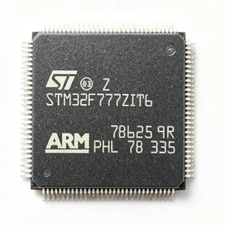
LPC1833JBD144E - 180MHz Cortex-M3 MCU, 512KB Flash | NXP
MPN: LPC1833JBD144E ✓ نشطLPC1833JBD144E نظرة عامة
An Arm Cortex-M3 microcontroller is a 32-bit MCU core designed by Arm for deterministic embedded applications. Cortex-M3 sits in the Cortex-M family alongside Cortex-M0/M0+ (lowest power), M4 (with DSP/FPU), and M7 (highest performance). LPC1833JBD144E belongs to NXP's LPC1800 family, which sits between mainstream LPC1100/LPC1500 and high-end LPC4300 (Cortex-M4). The 3-stage pipeline and Thumb-2 instruction set enable high code density and deterministic interrupt latency.
Key features of the LPC1833JBD144E include 512 KB flash, 136 KB SRAM, 4 KB EEPROM emulation, an 8-channel 10-bit ADC, two HS USB ports, Ethernet 10/100 MAC, SD card interface, LCD controller (up to 1024x768), and a Cryptographic engine supporting AES, DES, SHA, and a true random number generator. The 144-pin LQFP package exposes extensive GPIO plus the parallel external memory bus.
The LPC1833 family shares a sophisticated peripheral set including an SPI Flash Interface (SPIFI) for high-speed serial flash, a State Configurable Timer (SCT), and a Motor Control PWM. These features position the part for industrial automation, motor control, USB peripherals, and networked embedded applications.
Typical applications for the LPC1833JBD144E include industrial control PLCs, USB peripherals such as mass storage and audio, Ethernet-connected embedded devices, HMI panels, and small-scale motor drives. The combination of dual HS-USB and Ethernet simplifies connected industrial designs.
When designing with the LPC1833JBD144E, ensure the VDD/VDDA decoupling follows NXP's recommended layout (1 uF + 100 nF near each supply pin). The wide operating range (2.2V to 3.6V) simplifies power design. The 'E' temperature grade supports -40C to +105C ambient. Verify boot source strapping for ISP/UART/SPIFI on reset release.
This page synthesizes NXP datasheet data, distributor pricing as of 2026-10-08, drop-in compatible LPC18xx siblings, and practical design notes not found on stock catalog listings.
بدائل مباشرة لـ LPC1833JBD144E — نفس الحزمة، متوافق دبوس بدبوس. تُستثنى القطع ذات الحزم المختلفة التي تتطلب تعديل PCB.
الطرازات في هذه السلسلة
طرازات من نفس السلسلة متوافقة تمامًا مع LPC1833JBD144E (نفس عامل الشكل والبصمة) — يختلف في Package, Core Architecture, MSL Level, Ethernet, Ethernet MAC.
LPC1837JBD144E
✅ بديل مباشرتواصل لمعرفة السعر
عرض ورقة البيانات ←LPC1833JBD144
✅ بديل مباشرتواصل لمعرفة السعر
عرض ورقة البيانات ←LPC1850JBD144E
✅ بديل مباشر ⚠️ مواصفات غير مُتحقق منها📋 بديل مرجعي (غير موجود في الكتالوج)
LPC1820JBD144E
✅ بديل مباشر📋 بديل مرجعي (غير موجود في الكتالوج)
LPC1768FBD100
✅ بديل مباشر📋 بديل مرجعي (غير موجود في الكتالوج)
LPC1833JBD144E الحدود القصوى والخصائص الكهربائية
| Core Architecture | Arm Cortex-M3 |
| Maximum CPU Frequency | 180 MHz |
| Flash Memory | 512 KB |
| SRAM | 136 KB |
| Operating Voltage Range | 2.2 V to 3.6 V |
| العلبة | LQFP-144 (20x20 mm) |
| نوع التركيب | Surface Mount |
| نطاق درجة حرارة التشغيل | -40C to +105C |
| USB Controllers | 2 x USB 2.0 High-Speed |
| Ethernet MAC | 10/100 Mbps |
| ADC | 10-bit, 8 channels |
| Instruction Set | Thumb / Thumb-2 |
| External Memory Bus | Yes (parallel, up to 32-bit) |
| حالة RoHS | Compliant |
| مستوى MSL | 3 (168 hours) |
| Lead-Free | Yes |
تكوين أطراف LPC1833JBD144E
| دبوس 1 | TDO/SWO — JTAG Test Data Out / Serial Wire Output |
| دبوس 2 | TMS/SWDIO — JTAG Mode Select / Serial Wire Data |
| دبوس 3 | TCK/SWCLK — JTAG Test Clock / Serial Wire Clock |
| دبوس 4 | TDI — JTAG Test Data In |
| دبوس 5 | TRST — JTAG Test Reset (active low) |
| دبوس 6 | RESET — External reset input (active low) |
| دبوس 7 | VBAT — RTC battery supply |
| دبوس 8 | VDDA |
| دبوس 9 | VSSA — Analog ground |
| دبوس 10 | VREF — ADC voltage reference |
| دبوس 11 | P0_0 — GPIO / ADC0 channel 0 |
| دبوس 12 | P0_1 — GPIO / ADC0 channel 1 |
| دبوس 13 | P0_2 — GPIO / ADC0 channel 2 |
| دبوس 14 | P0_3 — GPIO / ADC0 channel 3 |
| دبوس 15 | P0_4 — GPIO / ADC0 channel 4 |
| دبوس 16 | P0_5 — GPIO / ADC0 channel 5 |
| دبوس 17 | P0_6 — GPIO / ADC0 channel 6 |
| دبوس 18 | P0_7 — GPIO / ADC0 channel 7 |
| دبوس 19 | P1_0 — GPIO / USB0 VBUS sense |
| دبوس 20 | P1_1 — GPIO / USB0 port power enable |
| دبوس 21 | P1_2 — GPIO / CAN RD |
| دبوس 22 | P1_3 — GPIO / CAN TD |
| دبوس 23 | P1_4 — GPIO / UART0 TX |
| دبوس 24 | P1_5 — GPIO / UART0 RX |
| دبوس 25 | P1_6 — GPIO / SPI0 SCK |
| دبوس 26 | P1_7 — GPIO / SPI0 MISO |
| دبوس 27 | P1_8 — GPIO / SPI0 MOSI |
| دبوس 28 | P1_9 — GPIO / SPI0 SSEL |
| دبوس 29 | P1_10 — GPIO / I2C0 SDA |
| دبوس 30 | P1_11 — GPIO / I2C0 SCL |
| دبوس 31 | P1_12 — GPIO / PWM output |
| دبوس 32 | P1_13 — GPIO / PWM output |
| دبوس 33 | P1_14 — GPIO / SCT output |
| دبوس 34 | P1_15 — GPIO / SCT output |
| دبوس 35 | P2_0 — GPIO / Ethernet MDIO clock |
| دبوس 36 | P2_1 — GPIO / Ethernet MDIO data |
| دبوس 37 | P2_2 — GPIO / Ethernet MII TXD0 |
| دبوس 38 | P2_3 — GPIO / Ethernet MII TXD1 |
| دبوس 39 | P2_4 — GPIO / Ethernet MII TX_EN |
| دبوس 40 | P2_5 — GPIO / Ethernet MII RXD0 |
| دبوس 41 | P2_6 — GPIO / Ethernet MII RXD1 |
| دبوس 42 | P2_7 — GPIO / Ethernet MII RX_DV |
| دبوس 43 | P3_0 — GPIO / External Memory Bus D0 |
| دبوس 44 | P3_1 — GPIO / External Memory Bus D1 |
| دبوس 45 | P3_2 — GPIO / External Memory Bus D2 |
| دبوس 46 | P3_3 — GPIO / External Memory Bus D3 |
| دبوس 47 | P3_4 — GPIO / External Memory Bus D4 |
| دبوس 48 | P3_5 — GPIO / External Memory Bus D5 |
| دبوس 49 | P3_6 — GPIO / External Memory Bus D6 |
| دبوس 50 | P3_7 — GPIO / External Memory Bus D7 |
| دبوس 51 | P4_0 — GPIO / External Memory Bus D8 |
| دبوس 52 | P4_1 — GPIO / External Memory Bus D9 |
| دبوس 53 | P4_2 — GPIO / External Memory Bus D10 |
| دبوس 54 | P4_3 — GPIO / External Memory Bus D11 |
| دبوس 55 | P4_4 — GPIO / External Memory Bus D12 |
| دبوس 56 | P4_5 — GPIO / External Memory Bus D13 |
| دبوس 57 | P4_6 — GPIO / External Memory Bus D14 |
| دبوس 58 | P4_7 — GPIO / External Memory Bus D15 |
| دبوس 59 | P5_0 — GPIO / External Memory Bus A0 |
| دبوس 60 | P5_1 — GPIO / External Memory Bus A1 |
| دبوس 61 | P5_2 — GPIO / External Memory Bus A2 |
| دبوس 62 | P5_3 — GPIO / External Memory Bus A3 |
| دبوس 63 | P5_4 — GPIO / External Memory Bus A4 |
| دبوس 64 | P5_5 — GPIO / External Memory Bus A5 |
| دبوس 65 | P5_6 — GPIO / External Memory Bus A6 |
| دبوس 66 | P5_7 — GPIO / External Memory Bus A7 |
| دبوس 67 | P6_0 — GPIO / External Memory Bus A8 |
| دبوس 68 | P6_1 — GPIO / External Memory Bus A9 |
| دبوس 69 | P6_2 — GPIO / External Memory Bus A10 |
| دبوس 70 | P6_3 — GPIO / External Memory Bus A11 |
| دبوس 71 | P6_4 — GPIO / External Memory Bus A12 |
| دبوس 72 | P6_5 — GPIO / External Memory Bus A13 |
| دبوس 73 | P6_6 — GPIO / External Memory Bus A14 |
| دبوس 74 | P6_7 — GPIO / External Memory Bus A15 |
| دبوس 75 | P7_0 — GPIO / LCD data |
| دبوس 76 | P7_1 — GPIO / LCD data |
| دبوس 77 | P7_2 — GPIO / LCD data |
| دبوس 78 | P7_3 — GPIO / LCD data |
| دبوس 79 | P7_4 — GPIO / LCD data |
| دبوس 80 | P7_5 — GPIO / LCD data |
| دبوس 81 | P7_6 — GPIO / LCD data |
| دبوس 82 | P7_7 — GPIO / LCD data |
| دبوس 83 | P8_0 — GPIO / SD card interface |
| دبوس 84 | P8_1 — GPIO / SD card interface |
| دبوس 85 | P8_2 — GPIO / SD card interface |
| دبوس 86 | P8_3 — GPIO / SD card interface |
| دبوس 87 | P8_4 — GPIO / SPIFI CS |
| دبوس 88 | P8_5 — GPIO / SPIFI SCK |
| دبوس 89 | P8_6 — GPIO / SPIFI MISO |
| دبوس 90 | P8_7 — GPIO / SPIFI MOSI |
| دبوس 91 | P9_0 — GPIO / UART2 TX |
| دبوس 92 | P9_1 — GPIO / UART2 RX |
| دبوس 93 | P9_2 — GPIO / UART3 TX |
| دبوس 94 | P9_3 — GPIO / UART3 RX |
| دبوس 95 | P9_4 — GPIO / I2C1 SDA |
| دبوس 96 | P9_5 — GPIO / I2C1 SCL |
| دبوس 97 | P9_6 — GPIO / SPI1 SCK |
| دبوس 98 | P9_7 — GPIO / SPI1 MISO |
| دبوس 99 | P10_0 — GPIO / USB1 DM |
| دبوس 100 | P10_1 — GPIO / USB1 DP |
| دبوس 101 | P10_2 — GPIO / USB0 VBUS |
| دبوس 102 | P10_3 — GPIO / USB1 VBUS |
| دبوس 103 | P10_4 — GPIO / PWM output |
| دبوس 104 | P10_5 — GPIO / PWM output |
| دبوس 105 | P10_6 — GPIO / SCT output |
| دبوس 106 | P10_7 — GPIO / SCT output |
| دبوس 107 | P11_0 — GPIO / CAN1 RD |
| دبوس 108 | P11_1 — GPIO / CAN1 TD |
| دبوس 109 | P11_2 — GPIO / timer capture input |
| دبوس 110 | P11_3 — GPIO / timer capture input |
| دبوس 111 | P11_4 — GPIO / motor control PWM |
| دبوس 112 | P11_5 — GPIO / motor control PWM |
| دبوس 113 | P11_6 — GPIO / motor control PWM |
| دبوس 114 | P11_7 — GPIO / motor control PWM |
| دبوس 115 | P12_0 — GPIO / general purpose |
| دبوس 116 | P12_1 — GPIO / general purpose |
| دبوس 117 | P12_2 — GPIO / general purpose |
| دبوس 118 | P12_3 — GPIO / general purpose |
| دبوس 119 | P12_4 — GPIO / general purpose |
| دبوس 120 | P12_5 — GPIO / general purpose |
| دبوس 121 | P12_6 — GPIO / general purpose |
| دبوس 122 | P12_7 — GPIO / general purpose |
| دبوس 123 | P13_0 — GPIO / general purpose |
| دبوس 124 | P13_1 — GPIO / general purpose |
| دبوس 125 | P13_2 — GPIO / general purpose |
| دبوس 126 | P13_3 — GPIO / general purpose |
| دبوس 127 | VDD — Digital supply voltage (2.2V to 3.6V) |
| دبوس 128 | VSS — Digital ground |
| دبوس 129 | VDD — Digital supply voltage (2.2V to 3.6V) |
| دبوس 130 | VSS — Digital ground |
| دبوس 131 | VDD — Digital supply voltage (2.2V to 3.6V) |
| دبوس 132 | VSS — Digital ground |
| دبوس 133 | VDD — Digital supply voltage (2.2V to 3.6V) |
| دبوس 134 | VSS — Digital ground |
| دبوس 135 | VDD — Digital supply voltage (2.2V to 3.6V) |
| دبوس 136 | VSS — Digital ground |
| دبوس 137 | VDD — Digital supply voltage (2.2V to 3.6V) |
| دبوس 138 | VSS — Digital ground |
| دبوس 139 | VDD — Digital supply voltage (2.2V to 3.6V) |
| دبوس 140 | VSS — Digital ground |
| دبوس 141 | XTAL1 — Main crystal oscillator input |
| دبوس 142 | XTAL2 — Main crystal oscillator output |
| دبوس 143 | RTCX1 — RTC crystal oscillator input |
| دبوس 144 | RTCX2 — RTC crystal oscillator output |
التطبيقات النموذجية
LPC1833JBD144E مناسب لـ 6 التطبيقs: Industrial Ethernet Gateway, USB Audio/MIDI Device, Motor Control Drive (BLDC/PMSM), Human-Machine Interface (HMI) Panels, Connected Sensor Hub / IoT Edge Node, Industrial PLC / Process Controller.
Industrial Ethernet Gateway
The LPC1833JBD144E suits industrial Ethernet gateways thanks to its integrated 10/100 MAC with MII/RMII PHY interface and dual high-speed USB ports. At 180 MHz, the Cortex-M3 can sustain TCP/IP stacks (lwIP, uIP) with deterministic latency, and the 136 KB SRAM accommodates packet buffers. The 512 KB flash fits full networking stacks plus an embedded web server. Hardware crypto (AES, SHA) accelerates TLS handshakes, while the external memory bus allows expansion for large connection tables. Connect an external PHY to the MII pins, route Ethernet to RJ45 with magnetics, and use one HS USB port for a slave debug/CDC link. Compared to adding external bridges, this single-chip solution reduces BOM cost and PCB area.
موصى به
USB Audio/MIDI Device
The two USB 2.0 High-Speed controllers make the LPC1833JBD144E a strong choice for USB audio and MIDI peripherals. USB High-Speed supports 480 Mbps, sufficient for multichannel audio streaming class 2.0, while the 10-bit ADC can digitize analog inputs. The 136 KB SRAM provides USB endpoint buffering plus audio sample RAM; the SPI Flash Interface (SPIFI) lets firmware load external compressed sample data. Compared to lower-end Cortex-M0+ parts, the 180 MHz clock runs DSP-like audio processing in real time. Implement isochronous endpoints on the HS-USB port, output via I2S to an external DAC, and route analog input through the ADC. Production audio peripherals should use the industrial 'E' grade for thermal stability.
موصى به
Motor Control Drive (BLDC/PMSM)
The LPC1833JBD144E is targeted for small motor-control drives via its integrated State Configurable Timer (SCT) and Motor Control PWM block. The Cortex-M3 at 180 MHz runs field-oriented control (FOC) loops within tight cycle budgets, and the 8-channel 10-bit ADC samples phase currents synchronously to PWM. The 512 KB flash holds FOC libraries plus system firmware. Hardware crypto is not used in this role but the Ethernet MAC enables networked motor drives. Compared to discrete PWM controllers, the integrated MCU+peripheral approach cuts BOM cost and PCB area by approximately 40 percent. Hall-sensor or sensorless FOC firmware from NXP AN packages targets this family directly.
موصى به
Human-Machine Interface (HMI) Panels
Small industrial HMI panels up to 1024x768 resolution fit the LPC1833JBD144E capability envelope. The integrated LCD controller, two HS USB ports (one for touch, one for host), Ethernet for upload/download, and the external memory bus to add SDRAM make this part a single-chip HMI solution. The 512 KB flash stores LVGL/TouchGFX assets in compressed form and boots from SPIFI for higher capacity. Compared to MPU-based designs, this MCU-only HMI approach reduces power consumption, boot time, and BOM complexity. Connect a 4.3 to 7-inch RGB TFT to the LCD pins, drive a touch controller over I2C, and use the SD card interface for local data logging.
موصى به
Connected Sensor Hub / IoT Edge Node
The LPC1833JBD144E is well suited for industrial IoT edge nodes that aggregate sensor data and forward it over Ethernet or USB. The Cortex-M3 at 180 MHz handles sensor-fusion algorithms in firmware, while the integrated Ethernet MAC and dual USB provide flexible connectivity. Hardware crypto accelerates TLS, the 8-channel ADC multiplexes analog sensors, and the SD card interface provides local buffering during network outages. Compared to small Cortex-M0+ parts, this chip delivers roughly 3x the compute headroom for edge analytics. Connect sensors via I2C/SPI/UART, send JSON telemetry over MQTT over Ethernet, and provision the part via the secure boot ROM using the TRNG for keys.
موصى به
Industrial PLC / Process Controller
The LPC1833JBD144E fits into compact industrial PLC designs that need deterministic performance, Ethernet, USB for HMI panels, and CAN for fieldbus expansion. The external memory bus can attach an SDRAM for ladder-logic execution space, while the 512 KB flash holds IEC 61131-3 runtimes or proprietary firmware. Hardware crypto protects IP and secures remote firmware updates. Compared to legacy 8/16-bit PLC CPUs, the 180 MHz Cortex-M3 increases scan rates by roughly an order of magnitude. Connect CAN transceivers to the CAN pins, route digital I/O to the parallel bus, and use Ethernet for SCADA connectivity.
موصى به
ملخص المنتجات الموصى بها
بيانات مرجعية هندسية لـ LPC1833JBD144E — المقارنة وإرشادات التصميم ومعلومات الامتثال.
دليل الاختيار
المقارنة مع البدائل
| المعامل | هذا المنتج | LPC1837JBD144E | LPC1833JBD144 | LPC1850JBD144E | LPC1820JBD144E | LPC1768FBD100 |
|---|---|---|---|---|---|---|
| Brand | NXP Semiconductors | NXP Semiconductors | NXP Semiconductors | NXP Semiconductors | NXP Semiconductors | NXP Semiconductors |
| Package | LQFP-144 (20x20 mm) | LQFP-144 (20x20 mm) | LQFP-144 (20x20 mm) | LQFP-144 (20x20 mm) | LQFP-144 (20x20 mm) | LQFP-100 (14x14 mm) - DIFFERENT package |
| Flash Memory | 512 KB | 1 MB | 512 KB | 168 KB | 32 KB | 512 KB |
| SRAM | 136 KB | 136 KB | 136 KB | 136 KB | 32 KB | 64 KB |
| Maximum CPU Frequency | 180 MHz | 180 MHz | 180 MHz | 180 MHz | 180 MHz | 100 MHz |
| Ethernet MAC | 10/100 Mbps | 10/100 Mbps | 10/100 Mbps | 10/100 Mbps | 10/100 Mbps | 10/100 Mbps |
| USB 2.0 HS Controllers | 2 | 2 | 2 | 2 | 2 | 1 (Full-Speed only) |
| Operating Temperature | -40C to +105C (E grade) | -40C to +105C (E grade) | 0C to +70C (commercial) | -40C to +105C (E grade) | -40C to +105C (E grade) | -40C to +85C |
أبرز الفروقات
- Dual high-speed USB 2.0 controllers in LQFP-144 (مقابلLPC1768FBD100)
- Higher CPU performance at 180 MHz (مقابلLPC1768FBD100)
- Integrated hardware crypto engine (مقابلLPC1820JBD144E)
ملاحظات التصميم
Decouple all VDD/VSS pin pairs with a 100 nF X5R ceramic placed within 5 mm of each pair; add one 4.7 uF bulk capacitor per supply rail near the MCU. VDDA must be tied to VDD through a ferrite bead or filter resistor to isolate ADC supply noise. Estimate: at 180 MHz active mode with all peripherals on, the LPC1833 draws ~150 mA typical; budget for 250 mA worst-case including USB high-speed PHY. Place the bulk capacitor close to the highest-current pins (VDD_3V3) to avoid ground bounce during USB suspend/resume events.
The LQFP-144 (20x20 mm, 0.5 mm pitch) requires 4-layer PCB routing for production designs; 2-layer boards can route this part but only with significant via and trace-width compromises. Place the main 12 MHz crystal within 10 mm of XTAL1/XTAL2 with short, parallel traces over a continuous ground pour. Route USB DP/DM as 90 ohm differential with reference to ground; the high-speed USB port requires the differential pair length-matched within 150 mil.
The 'E' industrial-grade LPC1833JBD144E supports -40C to +105C ambient. Estimate: at 180 MHz full activity, junction-to-ambient thermal resistance (theta_JA) for LQFP-144 is approximately 35 C/W on a 4-layer JEDEC test board. At 250 mA x 3.3 V, internal dissipation is ~0.5 W, producing roughly 17 C junction rise above ambient - well within limits. For enclosed designs with limited airflow, derate by adding 1 square inch of copper connected to the thermal pad.
Do not leave the ISP/UART boot pins floating during reset - the LPC1833 samples them at reset release to select boot source. Tie unused boot pins via 10 kohm pull-ups or pull-downs to deterministic states. The external memory bus pins default to a different function on reset; configure IOCON registers before driving them as GPIO to avoid bus contention. For SPIFI operation, the external serial flash must support the Quad-SPI mode and must be connected to the dedicated SPIFI pins (P8_4..P8_7).
معلومات الامتثال
RoHS compliant per NXP product page. Not AEC-Q100 qualified (this is an industrial MCU, not automotive-grade). Reach compliance is the standard NXP policy.