The SK hynix H5AN8G6NCJR-VKC is a high-performance 8Gb CMOS Double Data Rate IV (DDR4) SDRAM organized as 512M x16, operating at a data rate of 2666 Mbps (PC4-2133) from a nominal 1.2V supply (1.14V to 1.26V range) in a compact 96-ball FBGA package. It draws a typical 28 mA (IDD2N) and 45 mA (IDD4R), making it a power-efficient choice for server main memory, networking equipment, HPC clusters, and embedded systems. Key reliability features include auto self-refresh, write leveling, CRC, dynamic ODT, and ZQ calibration. The part is lead-free and halogen-free with RoHS and REACH compliance, and its lifecycle status is active. As of 2026-09-14, XAIPART lists 99,999 units in stock with MOQ 1, priced from $79.55 per unit down to $60.00 at 1000 units. Check live pricing on the H5AN8G6NCJR-VKC product page.
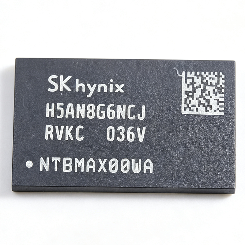
What Are the Verified Specifications of the H5AN8G6NCJR-VKC?
The table below consolidates every verified specification from the XAIPART product database, anchored to the SK hynix datasheet:
| Parameter | Value |
|---|---|
| Manufacturer | SK hynix |
| Memory Type | DDR4 SDRAM |
| Density | 8 Gb |
| Organization | 512M x 16 |
| Data Rate | 2666 Mbps (PC4-2133) |
| Supply Voltage (VDD) | 1.2 V (1.14V to 1.26V) |
| Operating Temperature | 0°C to +95°C (TC) |
| Package | FBGA-96, 0.8mm ball pitch |
| Operating Current (IDD2N) | 28 mA |
| Operating Current (IDD4R) | 45 mA |
| Burst Length | 8 (BC4) |
| Environmental | Lead-free, halogen-free, RoHS and REACH compliant |
| Lifecycle Status | Active |
Feature set verified from the datasheet includes programmable CAS latency, write leveling, dynamic on-chip termination (Dynamic ODT), ZQ calibration, CRC for data integrity, auto self-refresh, auto precharge, asynchronous reset, and data mask functions.
How Do You Design In the H5AN8G6NCJR-VKC?
Power Supply Design
Power the device from a regulated 1.2V rail that holds the 1.14V to 1.26V range across all load conditions, including the 45 mA IDD4R read-burst current. Decouple both VDD and VDDQ with 0.1uF and 1uF capacitors placed close to the balls, as the datasheet prescribes. VDDQ runs at the same voltage as VDD for the I/O interface.
Signal Integrity and Layout
Follow the DDR4 JEDEC standard (JESD79-4) for signal integrity and layout: use controlled impedance traces and matched lengths for the data, address, and command buses. The 0.8mm ball pitch of the FBGA-96 package enables high-speed signal routing on dense boards. Enable write leveling and dynamic ODT during controller initialization to compensate for trace-length mismatch on longer DIMM-style topologies.
Key Signal Connections
From the verified pinout: the differential clock pair CK (pin G2) and CK# (pin G3) connects to the memory controller. The data lane includes DQ0 through DQ7 (pins A2, B1, B3, C1, C3, D1, D3, E1), the differential data strobe DQS0 (pin E3) and DQS0# (pin F1), and the data mask DM0 (pin F3). Power pins include VDD at A1 and D2, VDDQ at B2, with VSS grounds at A3 and E2 and VSSQ I/O grounds at C2 and G1. The complete ball map is on the product page.
Worked Design Example: Bandwidth and Power Budget
One device delivers 8 Gb (1 GB) of memory. At the 2666 Mbps PC4-2133 rating on the 16-bit bus, theoretical bandwidth per device is 2666 Mb/s × 16 = 42,656 Mb/s ≈ 5.33 GB/s, transferring on both clock edges as a fully synchronous device referencing rising and falling edges of the clock. Quiescent power is 1.2 V × 28 mA = 33.6 mW; read-burst power is 1.2 V × 45 mA = 54 mW. A design using eight devices therefore supplies 8 GB of memory with roughly 43 GB/s of aggregate theoretical bandwidth while drawing only ~270 mW quiescent — an easy thermal fit for compact networking line cards and embedded controllers. For 0°C to +95°C ambient designs, validate board-level thermal dissipation within the verified TC range; for extended temperature ranges, the datasheet guidance points to automotive-grade DDR4 parts instead.
Procurement Notes
As of 2026-09-14, XAIPART stock stands at 99,999 units with MOQ 1. Volume tiers: $79.55 at qty ≥1, $75 at qty ≥10, $70 at qty ≥100, $65 at qty ≥500, and $60 at qty ≥1000. Plan board revisions against the active lifecycle status and re-verify stock at XAIPART before each build.
What Are the Best Alternatives to the H5AN8G6NCJR-VKC?
Only alternatives present in the XAIPART database are listed here. The Micron MT40A1G8SA-075E is a cross-brand, pin-compatible alternative with matching 8Gb DDR4 density and 2666 Mbps speed. The database also references the SK hynix H5AN8G6NDJR-XNC (same FBGA-96, faster 3200 Mbps grade) and the Samsung K4A8G165WB-BCRC as pin-compatible options; verify pin compatibility before substitution.
| Parameter | H5AN8G6NCJR-VKC | MT40A1G8SA-075E |
|---|---|---|
| Manufacturer | SK hynix | Micron |
| Memory Type | DDR4 SDRAM | DDR4 SDRAM |
| Density | 8 Gb | 8 Gb |
| Data Rate | 2666 Mbps (PC4-2133) | 2666 Mbps (speed grade 075E) |
| Relationship | Base product | Cross-brand pin-compatible alternative |
Qualification guidance: for a same-speed second source, the MT40A1G8SA-075E matches density and data rate. If your memory controller supports a faster grade and you want speed headroom, the H5AN8G6NDJR-XNC at 3200 Mbps is the pin-compatible upgrade path within the same FBGA-96 footprint — but confirm pin compatibility on your schematic before qualifying either substitute.
What Is the Market Position and Supply Situation for the H5AN8G6NCJR-VKC?
The H5AN8G6NCJR-VKC carries an active lifecycle status, confirming SK hynix continues to manufacture and support the part. DDR4 remains the industry-standard main memory for servers, desktops, laptops, and embedded systems, so this 8Gb, 2666 Mbps class of device sits squarely in mainstream demand for server DIMMs, networking line cards, and SoM designs. On the supply side, XAIPART holds 99,999 units in stock as of 2026-09-14 with MOQ 1, which covers both prototype orders and volume production runs at the $60 tier (qty ≥1000). Distributors such as LCSC, Octopart, and Worldway Electronics also list the part; LCSC shows it in stock while other channels may quote 4–8 week lead times, so confirm lead time with your distributor for production planning.
What Should Buyers Watch Next for DDR4 Memory Procurement?
Anchor your decisions to the verified specs and current availability of this part:
- Price tiers reward volume: unit cost falls from $79.55 (qty 1) to $60.00 (qty 1000) — a 25% reduction — so consolidating orders into 500+ or 1000+ quantities captures the best landed cost as of 2026-09-14.
- Speed headroom via pin-compatible upgrade: the FBGA-96-compatible H5AN8G6NDJR-XNC at 3200 Mbps lets future designs raise bandwidth ~20% over this part's 2666 Mbps without a footprint change, subject to pin-compatibility verification.
- Power budgets favor DDR4 at 1.2V: with 33.6 mW quiescent and 54 mW read power per device versus DDR3's 1.5V class, the verified 28 mA IDD2N and 45 mA IDD4R figures let you build denser memory pools inside fixed thermal envelopes.
- Environmental compliance is already covered: the part is lead-free, halogen-free, and RoHS/REACH compliant, simplifying regulatory sign-off for new designs.
- Temperature windows: at 0°C to +95°C (TC), confirm your end-application environment fits the verified range before committing; otherwise evaluate automotive-grade DDR4 per the datasheet's guidance.
For current stock, live pricing, and the full ball-map pinout, visit the H5AN8G6NCJR-VKC product page or browse all Memory ICs on XAIPART.
Comments
Be the first to comment.
🔐 Please sign in to post a comment.
Don't have an account? Sign up