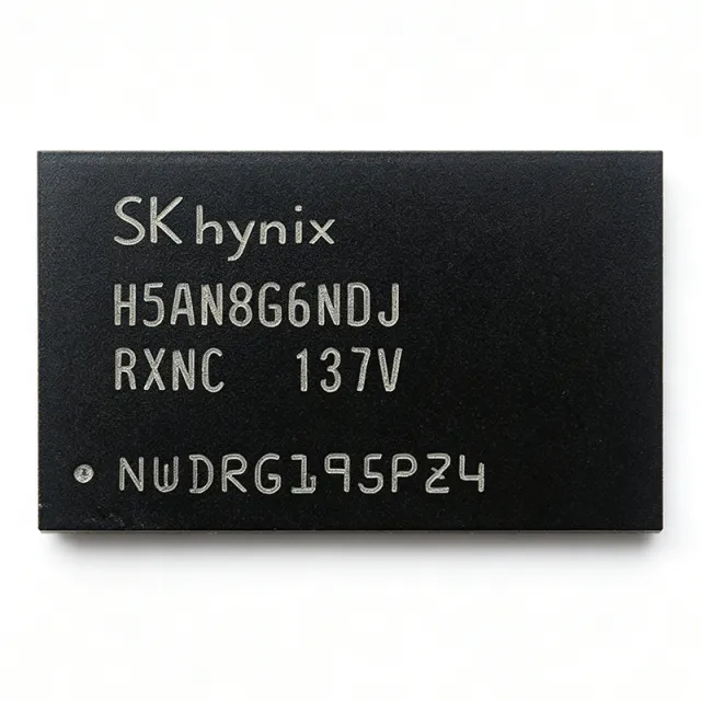
H5AN8G6NDJR-XNC - 8Gb DDR4-3200 x16 DRAM | SK Hynix
MPN: H5AN8G6NDJR-XNC ✓ Active| Qty | Unit Price | Extended |
|---|---|---|
| 1 | $95.4545 | $95.45 |
| 10 | $68.9394 | $689.39 |
| 100 | $60.9848 | $6,098.48 |
| 500 | $58.3333 | $29,166.65 |
| 1,000 | $55.6818 | $55,681.80 |
H5AN8G6NDJR-XNC Overview
DDR4 SDRAM is a type of volatile random-access memory that transfers data on both edges of the clock, doubling the data rate compared to DDR3. It operates at lower voltages (1.2V) and higher speeds, making it essential for modern computing systems, servers, and embedded applications. As a memory IC, it falls under the hierarchy of DRAM -> SDRAM -> DDR4 -> memory IC -> semiconductor, and is a critical component for data storage and processing.
Key features include a 512M x16 organization, 3200 Mbps data rate, 1.2V supply, and a 96-ball FBGA package. The device supports various functions such as auto self-refresh and ZQ calibration, which enhance reliability and signal integrity. The x16 interface allows for high bandwidth per chip, making it suitable for applications requiring wide data paths.
Technically, the H5AN8G6NDJR-XNC uses a CMOS process and is fully synchronous, with a differential clock (CK_t/CK_c) and on-die termination for improved signal quality. It supports burst lengths of 8 and 4, and includes a programmable read latency (RL) and write latency (WL) for system optimization. The device also features a temperature-compensated self-refresh (TCSR) to reduce power consumption.
Typical applications include laptop and desktop memory upgrades, industrial controllers, networking equipment, and embedded systems. Its high density and speed make it ideal for applications requiring large memory capacity and fast data access, such as AI edge devices and high-performance computing.
When designing with this component, ensure proper decoupling capacitors near the VDD and VDDQ pins, and follow the PCB layout guidelines for DDR4 routing to maintain signal integrity. The device is RoHS compliant and lead-free, making it suitable for environmentally conscious designs.
Drop-in alternatives for H5AN8G6NDJR-XNC — same package, pin-to-pin compatible. Different-package parts requiring PCB rework are excluded.
Variants in this series
Same-series models that are drop-in compatible with H5AN8G6NDJR-XNC (same form factor and footprint) — differing in Package, Data Rate, CAS Latency, Interface, Burst Length.
Quick Comparison Tool — Select alternative parts for side-by-side comparison:
H5AN8G6NAFR-UHC
✓ In Stock
$5.7422 / Unit
View Datasheet →K4A8G165WB-BCTD
✓ In Stock
$37 / Unit
View Datasheet →K4A8G165WB-BCRC
✓ In Stock
$12.57 / Unit
View Datasheet →MT40A512M16TB-062E:R
✓ In Stock
$60 / Unit
View Datasheet →H5AN8G6NCJR-XNC
📋 Reference alternative (not in catalog)
H5AN8G4NCJR-XNC
📋 Reference alternative (not in catalog)
H5AN8G6NDJR-XNC Maximum Ratings & Electrical Characteristics
| Memory Type | DDR4 SDRAM |
| Memory Size | 8 Gb |
| Memory Organization | 512M x16 |
| Data Rate | 3200 Mbps |
| Supply Voltage (VDD) | 1.2 V (max 1.26 V) |
| Package | FBGA-96 (13x7.5 mm) |
| Number of Terminals | 96 |
| Maximum Operating Temperature | 85 °C |
| Input/Output Type | COMMON |
| RoHS | Compliant |
| Lead-Free | Yes |
| Halogen Free | Yes |
| Auto Self-Refresh | Yes |
| Auto Precharge | Yes |
| Data Mask | Yes |
| Dynamic On-Chip Termination | Yes |
| ZQ Calibration | Yes |
| CRC Function | Yes |
| Write Leveling | Yes |
| Asynchronous Reset | Yes |
H5AN8G6NDJR-XNC Pin Configuration
| Pin A1 | VDD — Power supply |
| Pin A2 | DQ0 — Data input/output 0 |
| Pin A3 | DQ1 — Data input/output 1 |
| Pin B1 | VSS — Ground |
| Pin B2 | DQ2 — Data input/output 2 |
| Pin B3 | DQ3 — Data input/output 3 |
| Pin C1 | VDDQ — I/O power supply |
| Pin C2 | DQ4 — Data input/output 4 |
| Pin C3 | DQ5 — Data input/output 5 |
| Pin D1 | VSSQ — I/O ground |
| Pin D2 | DQ6 — Data input/output 6 |
| Pin D3 | DQ7 — Data input/output 7 |
| Pin E1 | CK_t — Clock (true) |
| Pin E2 | CK_c — Clock (complement) |
| Pin E3 | CKE — Clock enable |
| Pin F1 | CS_n — Chip select |
| Pin F2 | RAS_n — Row address strobe |
| Pin F3 | CAS_n — Column address strobe |
| Pin G1 | WE_n — Write enable |
| Pin G2 | A0 — Address input 0 |
| Pin G3 | A1 — Address input 1 |
Typical Applications
H5AN8G6NDJR-XNC is suitable for 6 applications: Laptop Memory Upgrade, Industrial Controllers, Networking Equipment, Embedded Systems, Data Storage Systems, Consumer Electronics.
Laptop Memory Upgrade
The H5AN8G6NDJR-XNC is an 8Gb x16 DDR4-3200 chip commonly used in laptops for memory upgrades. Its 3200 Mbps data rate and 1.2V operation provide high performance with low power consumption. The x16 interface simplifies PCB layout in space-constrained designs, making it ideal for thin and light notebooks. When upgrading, ensure compatibility with the system's memory controller and support for DDR4-3200 speed.
Recommended
Industrial Controllers
In industrial controllers, the H5AN8G6NDJR-XNC provides reliable high-density memory for data logging and real-time processing. Its auto self-refresh and ZQ calibration ensure stable operation over temperature variations. The 8Gb density allows for extended data buffering, while the 3200 Mbps speed supports fast data acquisition. The FBGA-96 package is suitable for compact industrial PCBs.
Recommended
Networking Equipment
The H5AN8G6NDJR-XNC is used in routers and switches for packet buffering and routing tables. Its high bandwidth (3200 Mbps) and low latency are critical for network throughput. The x16 organization provides a wide data path, reducing the number of chips needed. The device's CRC function enhances data integrity, which is essential for reliable network communication.
Recommended
Embedded Systems
For embedded systems, the H5AN8G6NDJR-XNC offers a balance of density and speed. Its 8Gb capacity supports complex applications like real-time operating systems and edge computing. The 1.2V supply reduces power consumption, extending battery life in portable devices. The device's small FBGA-96 package is ideal for space-constrained designs.
Recommended
Data Storage Systems
In data storage systems, the H5AN8G6NDJR-XNC serves as cache memory for SSDs and RAID controllers. Its high speed (3200 Mbps) and low latency improve I/O performance. The 8Gb density allows for large cache sizes, reducing the need for frequent disk access. The device's auto self-refresh helps maintain data integrity during idle periods.
Recommended
Consumer Electronics
The H5AN8G6NDJR-XNC is used in smart TVs, set-top boxes, and gaming consoles for system memory. Its 3200 Mbps data rate supports high-resolution video streaming and gaming. The x16 interface simplifies PCB design, reducing manufacturing costs. The device's low power consumption is beneficial for energy-efficient consumer devices.
Recommended
Engineering reference data for H5AN8G6NDJR-XNC — comparison, design guidance, and compliance information.
Selection Guide
Comparison with Alternatives
| Parameter | This Product | H5AN8G6NCJR-XNC | H5AN8G6NAFR-UHC | K4A8G165WB-BCTD |
|---|---|---|---|---|
| Package | FBGA-96 (13x7.5 mm) | FBGA-96 (13x7.5 mm) | FBGA-96 (13x7.5 mm) | FBGA-96 (13x7.5 mm) |
| Brand | SK Hynix | SK Hynix | SK Hynix | Samsung |
| Memory Size | 8 Gb | 8 Gb | 8 Gb | 8 Gb |
| Memory Organization | 512M x16 | 512M x16 | 512M x16 | 512M x16 |
| Data Rate | 3200 Mbps | 3200 Mbps | 3200 Mbps | 3200 Mbps |
| Supply Voltage | 1.2 V | 1.2 V | 1.2 V | 1.2 V |
| RoHS | Compliant | Compliant | Compliant | Compliant |
| Operating Temperature | 0°C to 85°C | 0°C to 85°C | 0°C to 85°C | 0°C to 85°C |
Key Differentiators
- High density 8Gb in x16 organization (vs H5AN4G8NBJR-VKI)
- DDR4-3200 speed grade (vs H5AN8G6NCJR-XNC)
- Cross-brand compatibility with Samsung K4A8G165WB-BCTD (vs K4A8G165WB-BCTD)
Design Notes
For DDR4 routing, maintain 50-ohm single-ended impedance for data lines and 100-ohm differential for clock signals. Keep trace lengths matched within 10 mils for data groups. Place decoupling capacitors (0.1uF and 1uF) close to VDD and VDDQ pins to minimize power supply noise.
The H5AN8G6NDJR-XNC has a maximum operating temperature of 85°C. Ensure adequate airflow or heatsinking in high-ambient environments. The FBGA-96 package has a thermal resistance that should be considered; refer to the datasheet for theta_JA values. For high-density systems, consider thermal vias under the package.
Use on-die termination (ODT) settings as recommended in the datasheet to reduce signal reflections. The dynamic on-chip termination feature helps maintain signal integrity at high speeds. Ensure proper termination for address and control lines. Follow the DDR4 layout guidelines for routing and spacing to minimize crosstalk.
Compliance Information
RoHS compliant and lead-free per JLCPCB and Alldatasheet. Halogen-free per Alldatasheet. AEC-Q100 not applicable for memory ICs.



