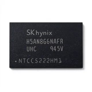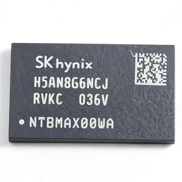
H5AN8G6NCJR-VKC - 8Gb DDR4 SDRAM 2666Mbps | SK Hynix
MPN: H5AN8G6NCJR-VKC ✓ Active| Qty | Unit Price | Extended |
|---|---|---|
| 1 | $79.55 | $79.55 |
| 10 | $75 | $750.00 |
| 100 | $70 | $7,000.00 |
| 500 | $65 | $32,500.00 |
| 1,000 | $60 | $60,000.00 |
H5AN8G6NCJR-VKC Overview
DDR4 SDRAM is the fourth generation of double data rate synchronous dynamic random-access memory, succeeding DDR3. It offers higher speed, lower operating voltage (1.2V vs 1.5V for DDR3), and improved signal integrity through on-die termination (ODT) and data bus inversion (DBI). DDR4 is the industry standard for main memory in servers, desktops, laptops, and embedded systems, providing the bandwidth and capacity required for modern computing workloads.
Key features include a burst length of 8 (BL8) with burst chop (BC4), programmable CAS latency, write leveling, dynamic on-chip termination (Dynamic ODT), ZQ calibration, and CRC (cyclic redundancy check) for data integrity. The device supports auto self-refresh, auto precharge, asynchronous reset, and data mask functions, ensuring reliable operation in demanding environments. It operates over a temperature range of 0°C to +95°C (TC), making it suitable for commercial and industrial applications.
The H5AN8G6NCJR-VKC utilizes advanced CMOS process technology, achieving low power consumption with a typical operating current of 28mA (IDD2N) and 45mA (IDD4R). The 96-ball FBGA package provides excellent thermal and electrical performance, with a ball pitch of 0.8mm, enabling high-speed signal routing. The device is lead-free and halogen-free, complying with RoHS and REACH regulations.
Typical applications include server main memory, networking switches and routers, high-performance computing (HPC), and embedded systems requiring high-density, high-bandwidth memory. The 2666 Mbps data rate and 8Gb density make it ideal for memory modules (DIMMs) and system-on-module (SoM) designs.
When designing with this device, ensure proper decoupling of the VDD and VDDQ supplies with 0.1uF and 1uF capacitors placed close to the balls. Follow the DDR4 JEDEC standard (JESD79-4) for signal integrity and layout guidelines, including controlled impedance traces and matched lengths for the data, address, and command buses.
Drop-in alternatives for H5AN8G6NCJR-VKC — same package, pin-to-pin compatible. Different-package parts requiring PCB rework are excluded.
Variants in this series
Same-series models that are drop-in compatible with H5AN8G6NCJR-VKC (same form factor and footprint) — differing in Package, Operating Temperature, Data Rate, RoHS Status, Burst Length.
Quick Comparison Tool — Select alternative parts for side-by-side comparison:
H5AN8G6NDJR-XNC
✓ In Stock
$55.6818 / Unit
View Datasheet →H5AN8G6NAFR-UHC
✓ In Stock
$5.7422 / Unit
View Datasheet →K4A8G165WB-BCRC
✓ In Stock
$12.57 / Unit
View Datasheet →NT5CC256M16ER-EKT
✓ In Stock
$22 / Unit
View Datasheet →W634GU6RB12I
✓ In Stock
$5.6 / Unit
View Datasheet →MT40A1G8SA-075E
📋 Reference alternative (not in catalog)
H5AN8G6NCJR-VKC Maximum Ratings & Electrical Characteristics
| Memory Type | DDR4 SDRAM |
| Density | 8 Gb |
| Organization | 512M x 16 |
| Data Rate | 2666 Mbps |
| Supply Voltage (VDD) | 1.2 V (1.14V to 1.26V) |
| Operating Temperature | 0°C to +95°C |
| Package | FBGA-96 |
| Operating Current (IDD2N) | 28 mA |
| Operating Current (IDD4R) | 45 mA |
| Burst Length | 8 (BC4) |
| Lead-Free | Yes |
| Halogen Free | Yes |
| RoHS | Compliant |
H5AN8G6NCJR-VKC Pin Configuration
| Pin A1 | VDD — Power supply |
| Pin A2 | DQ0 — Data input/output 0 |
| Pin A3 | VSS — Ground |
| Pin B1 | DQ1 — Data input/output 1 |
| Pin B2 | VDDQ — I/O power supply |
| Pin B3 | DQ2 — Data input/output 2 |
| Pin C1 | DQ3 — Data input/output 3 |
| Pin C2 | VSSQ — I/O ground |
| Pin C3 | DQ4 — Data input/output 4 |
| Pin D1 | DQ5 — Data input/output 5 |
| Pin D2 | VDD — Power supply |
| Pin D3 | DQ6 — Data input/output 6 |
| Pin E1 | DQ7 — Data input/output 7 |
| Pin E2 | VSS — Ground |
| Pin E3 | DQS0 — Data strobe 0 |
| Pin F1 | DQS0# — Data strobe 0 complement |
| Pin F2 | VDDQ — I/O power supply |
| Pin F3 | DM0 — Data mask 0 |
| Pin G1 | VSSQ — I/O ground |
| Pin G2 | CK — Clock |
| Pin G3 | CK# — Clock complement |
Typical Applications
H5AN8G6NCJR-VKC is suitable for 6 applications: Server Main Memory, Networking Equipment, High-Performance Computing (HPC), Embedded Systems, Data Center Storage, Telecommunications.
Server Main Memory
The H5AN8G6NCJR-VKC provides 8Gb density and 2666 Mbps data rate, making it ideal for server DIMMs. Its low 1.2V operation reduces power consumption in data centers. The high bandwidth supports virtualization, cloud computing, and big data analytics. When used in RDIMMs, the on-die termination and CRC ensure signal integrity over long traces. The 96-ball FBGA package allows high-density module designs, enabling larger memory capacity per server.
Recommended
Networking Equipment
In networking switches and routers, the H5AN8G6NCJR-VKC provides high-bandwidth memory for packet buffering and forwarding tables. Its 2666 Mbps data rate ensures low latency for high-throughput traffic. The auto self-refresh and low power modes help manage thermal budgets in compact chassis. The FBGA-96 package fits space-constrained line cards. The device's CRC and write leveling features enhance reliability in noisy environments.
Recommended
High-Performance Computing (HPC)
The H5AN8G6NCJR-VKC supports HPC applications requiring large memory capacity and high bandwidth. Its 8Gb density allows building high-capacity memory pools. The 2666 Mbps data rate provides fast data access for compute-intensive workloads. The low operating voltage reduces power consumption in large clusters. The device's advanced features like dynamic ODT and ZQ calibration ensure stable operation at high speeds.
Recommended
Embedded Systems
The H5AN8G6NCJR-VKC is suitable for embedded systems requiring high-density memory, such as industrial PCs and edge computing devices. Its 8Gb density provides ample memory for complex applications. The 0°C to +95°C temperature range covers most embedded environments. The FBGA-96 package is compact for space-limited designs. The device's low power consumption is beneficial for battery-powered or thermally constrained systems.
Recommended
Data Center Storage
In data center storage systems, the H5AN8G6NCJR-VKC provides high-bandwidth memory for caching and metadata management. Its 2666 Mbps data rate accelerates storage controllers. The low power consumption helps reduce operational costs. The device's reliability features, such as CRC and auto self-refresh, ensure data integrity. The FBGA-96 package enables high-density storage controller designs.
Recommended
Telecommunications
The H5AN8G6NCJR-VKC is used in telecom infrastructure for buffering and processing. Its high bandwidth supports 5G and edge computing workloads. The 1.2V operation reduces power in base stations. The device's wide temperature range and reliability features make it suitable for outdoor equipment. The FBGA-96 package allows compact line card designs.
Recommended
Recommended Products Summary
Engineering reference data for H5AN8G6NCJR-VKC — comparison, design guidance, and compliance information.
Selection Guide
Comparison with Alternatives
| Parameter | This Product | H5AN8G6NDJR-XNC | K4A8G165WB-BCRC | MT40A1G8SA-075E |
|---|---|---|---|---|
| Package | FBGA-96 | FBGA-96 | FBGA-96 | FBGA-96 |
| Brand | SK Hynix | SK Hynix | Samsung | Micron |
| Density | 8 Gb | 8 Gb | 8 Gb | 8 Gb |
| Data Rate | 2666 Mbps | 3200 Mbps | 2666 Mbps | 2666 Mbps |
| Supply Voltage | 1.2V | 1.2V | 1.2V | 1.2V |
| Operating Temperature | 0°C to +95°C | 0°C to +95°C | 0°C to +95°C | 0°C to +95°C |
| Lead-Free | Yes | Yes | Yes | Yes |
Key Differentiators
- Higher speed grade than base part (vs H5AN8G6NCJR-xxC)
- Cross-brand compatibility (vs K4A8G165WB-BCRC)
- Low power consumption (vs MT40A1G8SA-075E)
Design Notes
For DDR4 routing, maintain controlled impedance of 40-50 ohms for single-ended signals and 80-100 ohms differential for DQS and CK. Keep trace lengths matched within +/- 10 mils for data groups and +/- 20 mils for address/command. Use ground planes under the FBGA-96 package to minimize noise.
Decouple VDD and VDDQ with 0.1uF and 1uF capacitors placed as close as possible to the balls. Use a solid power plane for VDD and VDDQ. The 1.2V supply should have low impedance across the frequency range of interest to ensure stable operation at 2666 Mbps.
The H5AN8G6NCJR-VKC operates up to +95°C. Ensure adequate airflow or heatsinking in high-density designs. The FBGA-96 package has a thermal resistance that should be considered; refer to the datasheet for theta_JA. For high-power applications, consider thermal vias under the package.
Compliance Information
Lead-free and halogen-free per datasheet. RoHS compliant. Not AEC-Q100 qualified.