FPGA & CPLD
Products (6,800+)

XC3S50-5TQG144C - 50K Spartan-3 FPGA | AMD | 144-TQFP
The AMD XC3S50-5TQG144C is a Spartan-3 field-programmable gate array with 50,000 system gates, 1,728 logic cells, 97 I/O, a 1.2 V core supply, and a 144-pin TQFP package. Rated at up to 725 MHz, it targets compact programmable-logic designs that require more I/O and processing capacity than small CPLDs can provide. A field-programmable gate array is a semiconductor whose digital logic and interconnect are configured after manufacture. Within the product hierarchy, an FPGA is a programmable logic device and a semiconductor. The Spartan-3 family combines configurable logic blocks, programmable I/O, embedded block RAM, dedicated multipliers, and clock-management resources, allowing one device to implement control logic, data processing, interfaces, and small embedded systems. The XC3S50-5TQG144C combines 50,000 system gates with 1,728 logic cells and 97 available I/O in a 144-lead TQFP package. Its 1.2 V core supply reduces core power requirements, while the -5 speed designation corresponds to the 725 MHz maximum figure reported in the supplied product data. The commercial temperature range shown by the verified listings is 0°C to 85°C. This device is manufactured using 90 nm technology, positioning it as a cost-oriented, low-density FPGA rather than a high-performance FPGA with large on-chip memories. Configuration data programs the logic fabric and I/O standards, allowing hardware revisions and field updates without changing the printed circuit board. Because the package exposes many I/O in a relatively compact surface-mount format, PCB routing and power delivery remain central design constraints. Typical uses include industrial control, consumer electronics, embedded systems, communications interfaces, instrumentation, and general-purpose digital logic. Its 97 I/O make it particularly useful where external memory, parallel buses, status indicators, sensors, or multiple digital interfaces must connect to programmable logic. The 144-pin package also offers more I/O than a small PLD while remaining manageable for multilayer board assembly. Designers should verify the exact pinout, configuration interface, supported I/O standards, bank supply voltages, and decoupling requirements against the Spartan-3 manufacturer documentation before layout release. Because this is a legacy programmable-logic platform, toolchain availability, configuration-device compatibility, and long-term procurement should be confirmed during product planning. This page consolidates the verified distributor specifications, practical design considerations, and carefully qualified same-footprint alternatives for XC3S50-5TQG144C. It also distinguishes documented production options from unavailable or unverified engineering data so engineers can make a defensible sourcing and design decision.

XC3S50-5VQG100C - 50K Gate Spartan-3 FPGA | AMD
AMD XC3S50-5VQG100C is a Spartan-3 field-programmable gate array with 50,000 system gates, 1,728 logic cells, 63 programmable I/O pins, and a 1.2 V core supply in a 100-pin VTQFP package. It uses 90 nm CMOS technology and is rated for a maximum clock frequency of 725 MHz. A field-programmable gate array, or FPGA, is a semiconductor whose digital logic and I/O can be configured after fabrication. In the device hierarchy, an FPGA is a programmable logic device, followed by the broader categories of semiconductor, integrated circuit, and digital logic. Spartan-3 devices combine configurable logic blocks, distributed memory, dedicated input/output structures, and clocking resources in a single package. The XC3S50-5VQG100C provides 73,728 bits of distributed RAM and 192 logic array blocks, making its internal resources suitable for modest control systems, interface conditioning, signal processing, and embedded logic. Its 63 configurable I/O pins provide external connectivity, while the -5 speed designation corresponds to the verified 725 MHz maximum frequency. The 100-pin VTQFP package supports compact surface-mount PCB layouts. The Spartan-3 architecture uses a 90 nm process and a 1.2 V internal core voltage. Distributed RAM provides storage alongside configurable logic, allowing small lookup tables, buffers, and state machines to be implemented without relying entirely on external memory. Designers must also account for dedicated configuration pins, clock routing, power-supply sequencing, and the fixed resources assigned to configuration when planning the pinout. Typical uses include industrial control logic, low-cost embedded control, data acquisition, communication-interface bridging, instrumentation, and consumer electronics. The component is appropriate when a relatively small amount of parallel logic, moderate I/O connectivity, and programmable functionality are needed without moving to a larger FPGA. The primary design consideration is package and power planning. A 100-pin VTQFP layout is sensitive to thermal via placement and power-distribution integrity, while the 1.2 V core rail requires clean supply delivery. Configuration logic should also be preserved according to the manufacturer's guidance because its pins may not be freely available for ordinary user functions. This page combines the verified distributor specifications, package details, lifecycle caveat, drop-in replacement analysis, and practical design guidance for engineers evaluating the AMD Spartan-3 XC3S50-5VQG100C.

XC3S500E-4PQG208C - 500K Gate Spartan-3E FPGA | AMD
The AMD XC3S500E-4PQG208C is a Spartan-3E field-programmable gate array with 500,000 equivalent system gates, 10,476 logic cells, 1,164 configurable logic blocks, and 158 inputs in a 208-pin PQFP package. The device uses a 1.2 V supply and is identified by the provided data as supporting up to 572 MHz. It is a surface-mount programmable logic device for embedded control, signal processing, interface bridging, and parallel data acquisition systems. A field-programmable gate array, or FPGA, is a programmable digital logic device whose configurable logic and interconnect resources can be programmed after manufacture. FPGAs sit above fixed-function logic devices and programmable gate arrays in the digital-semiconductor hierarchy: a design can use programmable logic to implement counters, state machines, ALUs, control logic, and interface circuits without requiring a custom ASIC. Spartan-3E devices provide a practical balance between logic capacity, device cost, and design flexibility for embedded systems. The verified specifications identify the XC3S500E-4PQG208C as a 500K-gate Spartan-3E FPGA with 10,476 logic cells, 1,164 CLBs, 158 inputs, and a maximum clock frequency of 572 MHz. The 208-PQFP package provides a leaded, inspectable footprint for conventional surface-mount assembly. The C suffix and the verified distributor listings identify the exact commercial ordering code; the supplied sources do not provide a complete temperature-grade or lifecycle classification. This FPGA is suitable for control and sequencing logic where multiple parallel channels, counters, timers, and state machines must be implemented in one device. Its logic capacity can also support moderate data paths and protocol interfaces. The 572 MHz maximum clock figure should be treated as a device-level headline value; actual achievable clock rates depend on the selected I/O standard, timing constraints, routing, logic depth, and the external memory or transceiver interface. Typical applications include industrial automation, test-and-measurement front ends, communications adapters, embedded control systems, and signal-processing support. The package is particularly useful where a leaded package is preferred over a fine-pitch BGA and where the design requires a moderate number of I/O connections. Designers should verify board pinout, configuration requirements, power sequencing, I/O standards, and signal-integrity margins against the manufacturer datasheet before layout release. The principal design consideration is package-related routing and signal integrity. A 208-pin PQFP requires adequate copper clearances and controlled escape routing, especially for high-speed clock and interface nets. Configuration storage, bank supply voltages, decoupling, and pinout details must be implemented exactly as specified in the AMD Spartan-3E documentation. This page combines verified distributor and AMD documentation references with application guidance, lifecycle caveats, package-specific design notes, and explicitly qualified replacement analysis for engineers evaluating the XC3S500E-4PQG208C.

XC3S50A-4FT256C - 50K Spartan-3A FPGA | AMD | 256-FTBGA
AMD XC3S50A-4FT256C is a Spartan-3A field-programmable gate array with approximately 50,000 logic gates, 144 user I/O, and a 256-pin fine-pitch ball grid array package. The device operates from a 1.14 V to 1.26 V core-voltage range and is identified as a last-time-buy product. Its 4 speed grade supports cost-sensitive programmable logic applications where a compact, nonvolatile FPGA implementation is preferable to a fixed-function logic device. A field-programmable gate array is a semiconductor whose digital logic, interconnect, and input/output functions are configured after manufacture. Within the FPGA hierarchy, the Spartan-3A family belongs to the low-to-medium-density programmable-logic segment. The XC3S50A combines approximately 50,000 gates, 144 I/O, and a 256-ball FTBGA package in a surface-mount device suitable for compact embedded control, interface, data-capture, and industrial automation equipment. The available specifications identify 144 user I/O, a 1.14 V to 1.26 V core-voltage range, and an approximate gate count of 50,000. These resources support parallel control logic, protocol interfaces, glue logic, and modest embedded processing systems. The C suffix identifies the commercial product variant, while the -4 portion denotes the device speed grade. Detailed RAM, clock, configuration, and I/O standards were not present in the supplied verified data and must be confirmed from the AMD Spartan-3A family datasheet before design release. The XC3S50A-4FT256C is supplied in tray packaging according to the available product listing. Its 256-pin fine-pitch BGA format creates a compact land pattern but requires careful PCB layout, via-in-pad or via-under-bump considerations, and assembly processes capable of handling closely spaced balls. Signal-integrity, power-delivery, thermal, and exact package-dimension guidance should be taken directly from the AMD DS529 family document and the device pinout information. Typical uses include industrial automation controllers, instrumentation, embedded communications, consumer interfaces, and cost-sensitive control systems. Because the part is listed as last time buy, new production should include lifecycle review, planned end-of-life inventory, and a qualified second source. Lead time is listed as 12 weeks, making procurement planning essential for designs that cannot tolerate a supply interruption. Design engineers should verify the exact pinout, supported I/O standards, configuration interface, memory resources, and power requirements in the AMD Spartan-3A family datasheet before layout release. This page consolidates the supplied distributor data, lifecycle information, pricing references, drop-in family variants, and practical implementation considerations to support engineering selection.
XC3S50A-4FT256I - Spartan-3A 256-LBGA FPGA | AMD
The AMD XC3S50A-4FT256I is a Spartan-3A field-programmable gate array in a 256-ball, square, surface-mount LBGA package. The -4 suffix identifies the device speed grade, the FT code identifies the 256-ball package configuration, and the final I indicates industrial-temperature grading. Verified distributor information identifies the device as an FPGA with 144 I/O, 55,296 gates, and 1,584 logic cells. It is positioned for designs that require programmable digital logic, parallel interfaces, embedded control, and compact system integration. A field-programmable gate array is a semiconductor whose digital configuration is defined after fabrication. The FPGA category sits above programmable logic devices and below configurable digital system components, combining configurable logic blocks, programmable I/O, and dedicated resources in one integrated circuit. This hierarchy allows engineers to implement control, communications, data acquisition, signal processing, and interface logic on hardware that can be revised without changing the printed circuit board. The Spartan-3A family provides configurable logic blocks containing lookup tables and flip-flops, along with programmable general-purpose I/O and dedicated multiplier and accumulator resources in DSP48A slices. Those DSP48A resources are useful for multiply-accumulate operations, while the 144-I/O configuration supports systems with substantial external bus and control connectivity. The exact switching, timing, configuration-memory, and electrical limits must be confirmed in the AMD DS529 Spartan-3A family data sheet before a design is released. The XC3S50A-4FT256I is differentiated by its combination of the -4 performance grade, industrial-temperature grading, and 256-ball LBGA package. The industrial marking makes it more appropriate for temperature-controlled factory, telecom, and test equipment than a commercial-temperature alternative. The compact 17 x 17 mm package also supports dense board layouts, although its 256-ball geometry requires careful inspection and assembly planning. Typical applications include industrial automation, telecommunications, embedded instrumentation, data-acquisition systems, and compact control platforms. In these systems, the FPGA can consolidate parallel interface logic, perform protocol conversion, coordinate control sequencing, or implement DSP pipelines. Pairing it with an external data converter, communications transceiver, and nonvolatile configuration storage can produce a complete embedded processing subsystem. Designers should treat the 256-LBGA footprint as a demanding assembly constraint. The board should use an appropriate ball pitch and copper-compatible surface finish, while assembly planning must account for inspection, cleaning, placement, and solder-joint verification. Power rails, configuration sequencing, decoupling, clocking, and I/O standards should be designed from the complete AMD datasheet rather than inferred solely from the ordering code. This page combines verified distributor specifications, package data, and the AMD DS529 family reference with practical considerations that are not visible in a basic distributor listing. It also separates documented facts from parameters that still require schematic-level and board-level verification, helping engineers evaluate the XC3S50A-4FT256I for industrial FPGA designs without relying on assumptions.
XC3S50A-4TQ144C - 50K Spartan-3A FPGA | AMD/Xilinx
The AMD/Xilinx XC3S50A-4TQ144C is a Spartan-3A field-programmable gate array with 55,296 system gates, 1,584 logic elements, 108 user I/Os, and a 144-pin TQFP package. Designed for high-volume, cost-sensitive commercial applications, the device uses a 90 nm process technology and a 1.2 V core. The “-4” grade identifies its performance speed grade, while the “C” suffix denotes the commercial temperature option. A field-programmable gate array, or FPGA, is a semiconductor whose digital logic, interconnect, and I/O resources are configured after manufacture. An FPGA sits within the programmable-logic hierarchy above simple fixed logic devices and below software-configured processors. Unlike a mask-programmable ASIC, an FPGA allows design revisions, field updates, and logic changes without fabricating a new custom chip. The XC3S50A-4TQ144C combines a moderate logic capacity with 108 user I/Os in a surface-mount TQFP package. The primary headline features are 55,296 system gates, 1,584 logic elements, and 108 user I/Os. Search results also describe the device as a 50,000-system-gate Spartan-3A FPGA. Its 144-pin TQFP package provides 108 user I/Os for external interfaces and board-level connections, making this device suitable for compact embedded systems requiring substantial parallel connectivity. The Spartan-3A architecture combines configurable logic, programmable I/O, dedicated memory resources, and clock-management resources within a single programmable device. The 90 nm fabrication process supports a compact and cost-sensitive implementation compared with larger, more complex programmable-logic devices. The device’s combination of moderate gate capacity and high I/O availability allows designers to consolidate control, interface, and state-machine functions without using a discrete combination of multiple smaller devices. Typical applications include industrial control, instrumentation, communications equipment, consumer peripherals, embedded control, and general-purpose I/O expansion. The 108 user I/Os are especially useful for systems that need parallel data acquisition, digital control, display interfaces, or external memory connections. In these designs, the FPGA can implement parallel processing and control logic while its configuration system preserves update flexibility. A primary design consideration is supply voltage and I/O compatibility. The available source material specifies a 1.2 V core but does not provide the complete recommended operating ranges, I/O standard options, configuration memory requirements, or power-loss configuration behavior. These values must therefore be confirmed against the complete manufacturer datasheet before schematic capture, pin assignment, and PCB layout are released. This product data consolidates verified distributor specifications, package information, pricing, availability, and same-family replacement options with practical selection guidance. It adds value beyond a basic distributor listing by separating confirmed parameters from missing technical data and explaining where each Spartan-3A option is appropriate.

XC3S50A-4TQ144I - 50K Spartan-3A FPGA | AMD/Xilinx
The AMD/Xilinx XC3S50A-4TQ144I is a Spartan-3A field-programmable gate array with 50,000 system gates, 1,584 configurable logic cells, 55,296 RAM bits, and 108 I/O in a 144-LQFP package. It operates from a 1.14 V to 1.26 V core supply and is specified for an industrial junction-temperature range of -40°C to 100°C. The -4 suffix identifies the device speed grade, while the TQ144 package designation identifies the surface-mount 144-lead package used by the XC3S50A family. A field-programmable gate array, or FPGA, is a semiconductor whose digital logic, interconnect, and I/O behavior can be programmed after manufacture. Within the product hierarchy, an FPGA is a programmable logic device and ultimately a semiconductor. Compared with a fixed-function application-specific integrated circuit, an FPGA allows parallel hardware functions, interface adaptation, and design revisions without changing the PCB. The Spartan-3A family is positioned for compact, cost-sensitive designs requiring moderate logic density and extensive user I/O. The Spartan-3A architecture provides five principal programmable functional elements, including configurable logic blocks, programmable interconnect, dedicated block RAM, input/output blocks, and configuration resources. Each configurable logic block contains four-input lookup tables and flip-flop resources for implementing combinational and sequential logic. The available 1,584 logic cells and 55,296 RAM bits support control logic, bus arbitration, low-speed communication interfaces, instrumentation, and general-purpose digital processing. With 108 I/O, the XC3S50A-4TQ144I offers more interface capacity than the smallest devices in the Spartan-3A family. The 144-LQFP package exposes those I/O along with configuration and power pins on a conventional surface-mount footprint. The 50,000-gate rating describes the family’s system-gate scale rather than a guaranteed clock rate, while the -4 speed designation and the manufacturer’s timing specifications determine actual performance. Configuration and pinout details should be verified against the DS529 family datasheet before PCB release. Typical applications include industrial control, telecommunications equipment, consumer electronics, embedded instrumentation, interface bridging, and low-density signal-processing systems. In each case, the combination of 1,584 logic cells, 55,296 RAM bits, 108 I/O, and a compact 144-lead package allows logic and interface functions to be consolidated without adopting a larger FPGA or a separate microcontroller for basic control tasks. Designers should preserve the required core-supply decoupling, use the manufacturer-recommended configuration interface, and confirm every signal’s I/O standard, drive strength, slew rate, and termination requirements against the DS529 datasheet. Programming tools, bitstream compatibility, and end-of-life considerations should also be reviewed because FPGA toolchains and family support evolve over time. This page consolidates verified distributor availability, package and resource details, drop-in replacement analysis, and practical design guidance into a compact engineering reference. It distinguishes documented device facts from parameters that still require manufacturer-data or board-level confirmation.
XC3S50A-4VQ100C - 50K Spartan-3A FPGA | AMD | 100-TQFP
AMD XC3S50A-4VQ100C is a Spartan-3A field-programmable gate array (FPGA) providing 1,584 logic cells, 55,296 RAM bits, 68 user I/Os, and approximately 50,000 logic gates in a 100-pin TQFP package. The device operates from a 1.14 V to 1.26 V core supply, uses 90 nm FPGA technology, and is implemented on a 0.667 GHz performance grade. A field-programmable gate array is a semiconductor device whose digital logic, memory, and I/O behavior are defined by a programmable configuration bitstream. An FPGA belongs to the programmable-logic hierarchy, alongside CPLDs, and provides reconfigurable parallel logic for cost-sensitive, I/O-intensive electronic products. Unlike a fixed-function application-specific integrated circuit, an FPGA can be reprogrammed during development or, where configuration technology permits, after deployment. The Spartan-3A family targets high-volume designs requiring moderate logic density. This device includes 176 configurable logic blocks, 68 user I/Os, and 55,296 bits of block RAM. Supported configuration approaches include Master Serial mode using platform flash PROM, Master SPI mode using commodity serial flash, BPI mode using commodity parallel flash, Slave Parallel mode using SelectMAP or a processor, and Slave Serial mode. These interfaces allow the configuration source and board-level design to be selected according to cost, density, and update requirements. The XC3S50A-4VQ100C is identified as a -4 speed-grade device with 667 MHz performance, a 1.2 V core, and a commercial operating-temperature range of 0°C to 85°C junction temperature. Its 100-terminal surface-mount package provides 68 user I/O positions according to the verified distributor data. Configuration data is retained externally in a PROM or flash device, so the FPGA's implemented logic is not fixed at manufacture. Typical uses include industrial control interfaces, communication adapters, instrumentation, test equipment, embedded control, and general-purpose programmable logic. Its 68 I/Os make it appropriate for parallel data acquisition, control, bridging, and interface-conversion designs where a small pin count, legacy 90 nm economics, and reconfigurability are more important than the density offered by newer FPGA families. The primary design consideration is that configuration storage, programming, clocking, decoupling, and I/O voltage compatibility must be planned before schematic capture. Designers should use the AMD Spartan-3A family data sheet for the exact package pinout and device-specific constraints, and should verify the selected configuration PROM against the supported bitstream and interface requirements. This page consolidates the verified AMD and distributor specifications, exact package and resource information, commercially sourced alternatives, and practical replacement-selection guidance. It is intended to help engineers identify whether the XC3S50A-4VQ100C remains appropriate for an existing Spartan-3A design without overlooking temperature-grade or speed-grade differences.

XC3S50A-4VQ100I - 50K Spartan-3A FPGA | AMD | Industrial
AMD XC3S50A-4VQ100I is a Spartan-3A field-programmable gate array with 50,000 system gates, 1,584 logic cells, 68 user I/Os, and a maximum stated performance of 667 MHz, supplied in a 100-pin TQFP package. The device operates from a 1.2 V core supply and is specified for industrial-temperature use from -40°C to +100°C. A Spartan-3A FPGA is a programmable logic device within the broader semiconductor and FPGA hierarchy. Unlike a fixed-function application-specific integrated circuit, it combines configurable logic, programmable interconnect, memory resources, and general-purpose I/O. Its 100-pin TQFP package makes it suitable for designs requiring moderate logic density and external peripheral connectivity without using a large ball-grid-array package. The XC3S50A-4VQ100I provides 1,584 logic cells and 68 I/Os, allowing designers to implement control logic, interface protocols, data acquisition, or embedded state machines in one programmable device. The -4 speed designation identifies its performance grade, while the I suffix identifies the industrial-temperature option reported in the verified product data. The 90 nm fabrication process and 1.2 V core supply are consistent with the Spartan-3A generation. Its architecture supports configuration from several serial and parallel memory interfaces, including Master Serial, Master SPI, BPI, Slave Parallel, SelectMAP, and Slave Serial modes. Configuration storage can therefore use commodity serial flash, parallel flash, or platform flash, depending on board-level requirements. The exact configuration file size, supported I/O standards, and recommended termination network are not included in the supplied source snippets. Typical uses include industrial automation, communications equipment, test and measurement systems, embedded control, and I/O-intensive consumer or industrial products. The 68 available I/Os support external sensors, displays, memory devices, and communications transceivers, while the 50K-gate device size is appropriate for moderate parallel logic rather than high-throughput processor applications. Design planning should include correct configuration-pin connections, suitable bypass capacitors, and a verified JTAG programming chain. The 100-TQFP footprint also requires careful escape routing for fine-pitch leads and adequate board area for power distribution. Because a detailed pin map and current pricing were not present in the supplied data, the package pinout is intentionally left unavailable and the commercial tiers require a current quotation. This product record consolidates verified distributor specifications, same-family drop-in candidates, application guidance, and practical FPGA design considerations. It is intended to help engineers assess package compatibility, configuration strategy, thermal requirements, and procurement without substituting unsupported electrical or lifecycle assumptions.

XC6SLX100-2CSG484C - 101K Logic FPGA | AMD
The AMD XC6SLX100-2CSG484C is a Spartan-6 LX family Field Programmable Gate Array (FPGA) with 101,261 logic cells, 338 user I/Os, and 4,939,776 RAM bits. The device is housed in a lead-free 484-CSPBGA (19x19 mm, 0.80 mm pitch) surface-mount package and operates from a 1.14V to 1.26V core supply. This configuration delivers a compact, high-density programmable logic solution for commercial-temperature (0C to 85C) systems. What is an FPGA? A Field Programmable Gate Array is an integrated circuit whose logic fabric can be configured after manufacturing to implement arbitrary digital functions. FPGAs sit above CPLDs in capacity and are often used for parallel processing, protocol bridging, and hardware acceleration. In a system hierarchy, the Spartan-6 LX family belongs to programmable logic devices, a subset of integrated circuits, and is widely used in communications, industrial automation, and video processing. Key features of XC6SLX100-2CSG484C include 7,911 CLBs, an internal frequency up to 667 MHz, 338 user configurable I/O pins, and 4,939,776 total block RAM bits. The -2 speed grade balances performance and power for cost-sensitive designs. The 484-ball CSPBGA package provides a 19x19 mm footprint with 0.80 mm pitch, making it suitable for space-constrained PCBs. Beneath the package, the Spartan-6 LX100 uses a 45nm CMOS process technology. This process enables high logic density and low static power, with core voltage around 1.2V. The FPGA includes dedicated clock management tile, DSP slices, and block RAM resources that can be used to build efficient digital signal processing pipelines, soft processors, and high-speed I/O interfaces. Typical applications include industrial automation controllers, telecom line cards, video and image processing, software-defined radio, and ASIC prototyping. The 338 I/O pins and abundant logic cells allow integration of multiple peripheral interfaces and custom processing engines on one device. When paired with DDR3 memory such as MT41K256M16HA-125:E or IS43TR16256AL-125KBL, the FPGA can implement high-bandwidth data buffers and packet processing. When designing with this component, plan the power delivery network carefully for the 1.14V to 1.26V core rail and respect the 0C to 85C junction temperature range. Decouple each supply pin and verify configuration memory selection before layout.

XC6SLX100-2FG484C - 101K-Logic Cell Spartan-6 FPGA | AMD
The AMD XC6SLX100-2FG484C is a Spartan-6 LX field-programmable gate array with 101,261 logic cells, 326 user I/O, and a 484-ball BGA package. It operates as a configurable parallel-processing semiconductor, combining programmable logic, block RAM, and digital clocking resources in one device. The package is identified by the verified distributor data as a 484-BBGA, and the Spartan-6 LX family is associated with 45 nm CMOS technology. A field-programmable gate array is a digital semiconductor whose logic, memory, and interconnect functions are configured after manufacture. An FPGA belongs to the programmable-logic hierarchy, which includes CPLDs, FPGA and CPLD devices, programmable-logic ICs, and semiconductors. Compared with a fixed-function application-specific integrated circuit, an FPGA allows parallel algorithms, interface protocols, timing, and control logic to be revised without changing the printed circuit board. The XC6SLX100-2FG484C provides 101,261 logic cells and 326 I/O in its 484-ball package. Verified family information reports an internal frequency of 667 MHz for the related 484-ball Spartan-6 LX ordering information. The -2 suffix identifies the device speed grade, while the FG484C portion identifies the package and commercial-temperature ordering code. These identifiers must be preserved when replacing the device because FPGA package pinouts, speed grades, and temperature ratings are not interchangeable by assumption. Its 101,261-cell capacity makes the device suitable for designs combining multiple parallel processing lanes rather than simple control functions. Available Spartan-6 LX resources can support high-throughput digital filtering, protocol bridging, embedded control, video-processing pipelines, and data acquisition when the design is implemented within the device's resource and speed limits. The 326 I/O count also provides substantial board-level connectivity, reducing the need for external interface components in systems that can use the available pins according to the AMD package pinout files. Typical applications include industrial automation, test and measurement equipment, communications interfaces, embedded video, robotics, and general-purpose instrumentation. Because the device is an FPGA rather than a microprocessor, firmware is not executed from a boot flash device. Instead, a bitstream defines the logic configuration and must be loaded into the FPGA according to the device's configuration architecture. Configuration storage, startup behavior, clocking, and JTAG access therefore remain important system-level design considerations. For reliable implementation, follow AMD's package pinout files and configuration guidance for the exact 484-ball land pattern. The board must also provide suitable decoupling, stable clocking, correct configuration startup behavior, and adequate power delivery. Although the verified listing identifies a 484-BBGA package, pin names and the complete 484-ball assignment are not included in the supplied data, so this page does not reproduce or infer them. This page combines verified distributor identification, price and availability references, package details, same-family drop-in candidates, and practical selection guidance. It also separates confirmed facts from parameters that require confirmation in the AMD Spartan-6 LX datasheet and official package files, helping engineers avoid unsupported substitutions.

XC6SLX100-2FGG676C - 101K LEs Spartan-6 LX FPGA | AMD Xilinx
The AMD Xilinx XC6SLX100-2FGG676C is a Spartan-6 LX family Field Programmable Gate Array (FPGA) with 101,261 logic cells, 4,939,776 system gates, and 480 I/O pins, housed in a 676-ball Fine-Pitch Ball Grid Array (FBGA-676) package with 0.8 mm ball pitch and a 19×19 mm body. The -2 speed grade targets mid-range performance and is fabricated on a 45 nm CMOS process with a 1.2 V core supply; commercial temperature grade (C suffix) supports 0 °C to +85 °C operation. What is an FPGA? An FPGA (Field Programmable Gate Array) is a semiconductor device whose logic fabric, interconnect, and I/O can be reconfigured by the designer after PCB assembly. The Spartan-6 LX position in the broader hierarchy is: programmable logic -> FPGA -> low-power FPGA family. Compared with ASICs, FPGAs trade raw unit cost for design flexibility, in-system reprogrammability, and rapid prototyping, and they sit in the same tier as CPLDs and complex PLDs for glue-logic and parallel DSP workloads. Key features include 3.8 Mb of block RAM, 180 DSP48A1 slices, integrated Memory Controller Blocks (MCBs), and up to 108 Mb of embedded memory. The device supports common interfaces such as DDR, DDR2, DDR3, LVDS, LVCMOS, and PCI Express endpoint via the integrated GTP transceiver infrastructure in compatible LXT variants. The XC6SLX100 offers a balanced cost/performance ratio ideal for high-volume, cost-sensitive designs requiring substantial logic density. The LX architecture uses a 6-input LUT fabric with dedicated carry logic, distributed RAM and shift-register resources, and a multi-clock tiles structure. The internal core can run up to approximately 667 MHz depending on speed grade, and high-speed SelectIO technology provides flexible I/O support for single-ended and differential standards at data rates into the hundreds of Mbps range. Typical applications include industrial motor control, LED video walls and digital signage, surveillance IP cameras, automotive driver assistance (non-safety-critical domains), consumer video processing, and small-cell baseband processing. The Spartan-6 LX family is widely used as a bridge between CPLD and higher-density Virtex-class FPGAs. When designing with this device, plan for a 1.2 V core rail and a 2.5 V/3.3 V auxiliary supply, with I/O voltages per bank. Use Xilinx ISE Design Suite (or Vivado with legacy project import) for bitstream generation; the FBGA-676 footprint demands careful PCB stack-up and via-in-pad escape routing. This page synthesizes distributor pricing, drop-in alternatives within the Spartan-6 and competing Cyclone IV families, and practical PCB design guidance not found in a single source datasheet.
XC6SLX100-3FGG484C Spartan-6 LX FPGA 101K Cells | AMD Xilinx
The AMD Xilinx XC6SLX100-3FGG484C is a Spartan-6 LX Field Programmable Gate Array (FPGA) delivering 101,261 logic cells, 4,939,776 system gates, and 326 user I/O in a 484-ball Fine-pitch BGA package with -3 (highest performance) speed grade. An FPGA (Field Programmable Gate Array) is a semiconductor device whose logic function is defined by the customer after manufacture, rather than at the fab. FPGAs sit in the broader hierarchy of programmable logic devices (PLD) -> CPLD -> FPGA -> SoC FPGA, and combine configurable logic blocks (CLBs), programmable routing, dedicated DSP slices, Block RAM, and hardened I/O serializers. Unlike microcontrollers (which execute instructions sequentially), FPGAs perform true parallel datapath operations, making them the preferred choice for high-throughput DSP, packet processing, and custom interface bridging where latency and determinism matter more than raw CPU clock rate. The XC6SLX100-3FGG484C integrates 180 DSP48A1 slices for fixed- and floating-point acceleration, 4,824 Kbits of Block RAM, four clock management tiles (CMTs) with PLL/DLL, and SelectIO technology supporting voltages from 1.2V to 3.3V. The -3 speed grade delivers the highest Fmax in the Spartan-6 LX family, while the 45 nm process node keeps static power in the milliwatt range compared to older 90/65 nm nodes. Typical applications include high-volume consumer and industrial designs such as video processing pipelines, motor control, industrial Ethernet bridges, PCIe endpoint controllers (when paired with an external PHY), and digital signage. Designers also use it for custom packet processors in telecom backhaul equipment and as a flexible I/O expander/glue logic replacement for multiple CPLDs on a single board. When designing with the -3 speed grade, ensure your PCB footprint supports the FGG484 (Pb-free, 1.0 mm pitch, 19 x 19 mm body) BGA land pattern and provide adequate via-in-pad or microvia escape routing. Decoupling must follow the Spartan-6 PCB Design Guide for the VCCINT, VCCAUX, and VCCO rails to meet the -3 timing closure across the full industrial temperature range. This page synthesizes distributor pricing, verified drop-in same-family and cross-brand Spartan-6 equivalents, and practical board-level design guidance that is not consolidated in the manufacturer datasheet itself.
XC6SLX100T-2CSG484I - Spartan-6 FPGA 101K Logic Cells | AMD
The AMD XC6SLX100T-2CSG484I is a member of the Spartan-6 LXT FPGA family, built on a mature 45nm low-power copper process technology. It delivers 101,261 logic cells and 296 user I/O pins in a 484-ball CSBGA package, offering a balance of density, performance, and low power for high-volume applications. The device operates from a 1.2V core supply and supports a wide range of I/O standards. An FPGA (Field-Programmable Gate Array) is an integrated circuit that can be configured by the designer after manufacturing, allowing for custom digital logic implementations. FPGAs sit between ASICs and microprocessors in the design hierarchy, providing reconfigurable hardware acceleration for tasks ranging from protocol bridging to digital signal processing. The Spartan-6 family is optimized for cost-sensitive, high-volume applications where low power and system integration are critical. Key features of the XC6SLX100T-2CSG484I include 4,939,776 bits of block RAM, 268 DSP48A1 slices, and support for high-speed serial transceivers (up to 3.125 Gbps) in the LXT variant. The device also includes a hard PCI Express block, memory controllers, and advanced clock management tiles (CMTs) with PLLs and DCMs. These features enable the implementation of complete system-on-chip designs with minimal external components. From a technical perspective, the Spartan-6 family uses a 45nm process that reduces dynamic power consumption by approximately 50% compared to previous Spartan families. The fabric is based on a 6-input look-up table (LUT) architecture, providing efficient logic utilization. The device supports partial reconfiguration, allowing dynamic updates to logic functions without powering down the system. Typical applications include industrial automation, automotive infotainment, medical imaging, and communications equipment. The 296 I/O pins support various standards including LVCMOS, LVDS, and HSTL, making it suitable for interfacing with a wide range of peripherals and memory devices. When designing with this FPGA, careful attention to power supply decoupling and thermal management is essential. The 1.2V core supply should be regulated with low-noise LDOs or switching converters, and the device's power consumption should be estimated using the Xilinx Power Estimator (XPE) tool to ensure adequate cooling.

XC6SLX100T-3FGG484C - Spartan-6 FPGA 101K Logic Cells | AMD
The AMD XC6SLX100T-3FGG484C is a member of the Spartan-6 LXT family of Field Programmable Gate Arrays (FPGAs), built on a mature 45 nm low-power copper process technology. It delivers 101,261 logic cells, 296 user I/O pins, and 4,939,776 bits of block RAM, all in a 484-ball FBGA package. This device is designed for high-volume applications requiring leading system integration with the lowest total cost, offering half the power consumption of previous Spartan families and faster, more comprehensive connectivity. An FPGA (Field Programmable Gate Array) is an integrated circuit that can be configured by the customer or designer after manufacturing—hence 'field-programmable'. FPGAs are part of the broader category of programmable logic devices (PLDs), which sit between application-specific integrated circuits (ASICs) and general-purpose processors in the semiconductor hierarchy. They consist of an array of programmable logic blocks, interconnects, and I/O blocks, allowing designers to implement custom digital logic circuits without the high NRE costs of ASIC development. FPGAs are widely used in prototyping, aerospace, automotive, industrial, and communications applications where flexibility and time-to-market are critical. Key features of the XC6SLX100T-3FGG484C include 101,261 logic cells, 296 user I/O pins, 4,939,776 bits of block RAM, and support for various I/O standards including LVCMOS, LVDS, and HSTL. The device operates from a 1.2V core voltage and is available in the -3 speed grade, which is the fastest speed grade for this part. The 484-ball FBGA package measures 23x23 mm with a 1.0 mm ball pitch, providing a compact footprint for dense PCB designs. The device also includes advanced clock management tiles (CMTs) with PLLs and DCMs, and supports configuration via JTAG, SPI, and BPI interfaces. From a technical depth perspective, the Spartan-6 family is built on a 45 nm low-power copper process, which balances performance and power efficiency. The LXT variant includes high-speed serial transceivers (up to 3.125 Gbps), PCI Express endpoints, and advanced memory controllers, making it suitable for high-bandwidth applications. The device also features dedicated DSP48A1 slices for digital signal processing, providing up to 180 GMACs of performance. The -3 speed grade offers the highest performance, with maximum clock frequencies typically exceeding 400 MHz for internal logic. Typical applications for the XC6SLX100T-3FGG484C include software-defined radio (SDR), industrial motor control, medical imaging, and high-performance computing acceleration. Its combination of logic density, I/O count, and transceiver capabilities makes it ideal for bridging, protocol conversion, and real-time signal processing tasks. The device is also well-suited for aerospace and defense applications where long-term supply and traceability are required. When designing with this FPGA, careful attention must be paid to power supply decoupling and PCB layout. The core voltage (VCCINT) should be regulated at 1.2V with low-noise LDOs or switching regulators, and each power pin should have a 100 nF ceramic capacitor placed as close as possible. Additionally, the configuration bitstream must be stored in an external SPI flash or programmed via JTAG, and the device supports multi-boot for remote updates.
XC6SLX150-3FGG676C - Spartan-6 LX FPGA 147K LE | AMD Xilinx
The AMD Xilinx XC6SLX150-3FGG676C is a Spartan-6 LX family Field-Programmable Gate Array (FPGA) delivering 147,443 logic cells, 23038 Adaptive Logic Modules (ALMs), and 4,939,776 system gates in a 676-ball Fine-Pitch Ball Grid Array (FGG676) package. It carries the -3 commercial speed grade with a maximum core clock of 862 MHz, offers 498 user I/Os, and operates over the commercial 0C to +85C temperature range per the FBGA-676 27 x 27 mm, 1.0 mm pitch package profile. An FPGA (Field-Programmable Gate Array) is a type of programmable logic device (PLD) that combines logic gates, multipliers, embedded memory, and high-speed transceivers into a configurable fabric. FPGA sits in the hierarchy of programmable logic -> programmable logic device -> semiconductor -> integrated circuit. The Spartan-6 LX family targets high-volume cost-sensitive applications that demand high logic density, abundant block RAM, and integrated DSP slices without the power overhead of Virtex-class devices. By programming the LUTs, routing, and IP cores via the ISE Design Suite, engineers create custom accelerators, glue logic, video pipelines, and connectivity subsystems on a single chip. Key features of the XC6SLX150-3FGG676C include 135 Kbit distributed RAM, 4.8 Mbit block RAM, 180 DSP48A1 slices, four clock management tiles with PLL, and 498 SelectIO signals supporting LVCMOS, LVDS, and LVTTL standards. The device integrates PCI Express Endpoint blocks, GTP transceivers are NOT present on this LX variant, and supports DDR, DDR2, DDR3, and QDRII+ memory interfaces through dedicated hardware controllers. Configuration is via SPI, BPI, JTAG, or Platform Flash XCF, enabling flexible in-system reprogrammability for field upgrades. From a system-architecture perspective, the Spartan-6 LX uses a 45 nm copper CMOS process backed by an optimized core voltage of 1.14 to 1.26 V and auxiliary supply of 2.5 / 3.3 V for I/O banks. The 676-BGA package exposes 26 user I/O banks so designers can support mixed-voltage interfaces (1.2 V to 3.3 V) on a single die, ideal for bridging legacy and modern logic families in industrial control or motor-drive boards. Typical applications include industrial motor control and factory automation backbones, video surveillance processing pipelines, medical imaging front-end buffers, automotive driver-assistance pre-processing prototypes, and avionics display controllers. The combination of abundant I/O and large block RAM makes the LX150 particularly attractive for high-channel-count data acquisition and parallel sensor aggregation. When designing with this part, validate that the 676-BGA layout supports at least four routing layers with laser-drilled microvias, since 1.0 mm pitch BGA escape routes demand controlled-impedance planning. Also confirm that the ISE WebPACK license covers all required IP cores for development. This page synthesizes distributor availability, drop-in Spartan-6 family alternatives, and practical layout notes not bundled into the manufacturer datasheet.
XC6SLX150T-3FGG484I - Spartan-6 LXT FPGA 147K Logic Cells | AMD
The AMD XC6SLX150T-3FGG484I is a high-performance Field Programmable Gate Array (FPGA) from the Spartan-6 LXT family, built on a 45nm CMOS process technology. It delivers 147,443 logic cells and 23,038 adaptive logic modules (ALMs) in a 484-pin FBGA package with a 19x19 mm body and 0.80 mm pitch. The device operates from a 1.2V core supply and supports up to 296 user I/O pins, making it suitable for high-volume, cost-sensitive applications requiring substantial logic density and I/O flexibility. An FPGA (Field Programmable Gate Array) is a semiconductor device containing a matrix of configurable logic blocks (CLBs) and programmable interconnects that can be programmed after manufacturing to implement arbitrary digital logic functions. FPGAs sit within the broader hierarchy of programmable logic devices (PLDs), which themselves fall under the category of integrated circuits. Unlike fixed-function ASICs, FPGAs offer reconfigurability, enabling rapid prototyping, hardware acceleration, and in-field updates, which is critical for evolving standards and algorithm changes. Key features of the XC6SLX150T-3FGG484I include 4.71 Mbit of embedded block RAM, integrated DSP slices for signal processing, and support for multiple I/O standards including LVCMOS, LVDS, and HSTL. The -3 speed grade provides the highest performance within the Spartan-6 LXT family, with internal clock frequencies up to 667 MHz. The device also includes hardened memory controllers for DDR, DDR2, and DDR3, reducing system cost and design complexity. Technically, the Spartan-6 architecture employs a 45nm low-power copper process with a 1.2V core voltage, balancing performance and power consumption. The device integrates Clock Management Tiles (CMTs) containing DCMs and PLLs for robust clock generation and jitter filtering. The LXT variant adds high-speed serial transceivers (up to 3.125 Gbps) and PCIe endpoints, enabling advanced bridging and serial connectivity applications. Typical applications include automotive infotainment systems, industrial automation controllers, consumer electronics bridging, and high-speed data acquisition. The 296 I/Os and 4.71 Mbit memory make it ideal for video processing, motor control, and protocol conversion. The -3 speed grade ensures timing closure for demanding designs. When designing with this FPGA, careful attention to power supply decoupling is essential. Use multiple 100nF and 10uF capacitors near the VCCINT, VCCAUX, and VCCO pins to minimize noise. Additionally, configure the device's I/O standards to match the external interface voltages to prevent damage and ensure signal integrity.

XC6SLX16-2CPG196C - Spartan-6 LX 375 MHz FPGA | AMD
AMD/Xilinx XC6SLX16-2CPG196C is a Spartan-6 LX field-programmable gate array with 14,579 logic cells, 106 user I/Os, and a maximum stated operating frequency of 375 MHz, supplied in a 196-ball CSBGA package. The device operates from a 1.14 V to 1.26 V core-supply range and is built on 45 nm CMOS technology. It combines programmable logic, block RAM, digital clock managers, and PLL resources in a cost-sensitive FPGA platform for industrial and embedded systems. A field-programmable gate array is a semiconductor device whose digital behavior is configured through a programmable bitstream rather than a fixed circuit layout. Within the product hierarchy, an FPGA is a programmable logic device and semiconductor, while the Spartan-6 LX family combines configurable logic blocks and dedicated resources for parallel processing, control, signal generation, and interface bridging. The XC6SLX16-2CPG196C provides 14,579 logic cells, 106 user I/Os, 375 MHz stated operating performance, and 667 MHz internal frequency according to the verified product listings. Its 196-ball CSBGA footprint measures 19 mm by 19 mm with a 0.80 mm ball pitch. The commercial-temperature suffix C corresponds to the listed 0 °C to 85 °C operating range, while the -2 suffix identifies the device speed grade. Spartan-6 devices use configurable logic and dedicated resources to implement control logic, parallel data processing, memory-intensive functions, and communication bridges. The -2 grade provides a practical balance between processing performance and cost, making the LX16 suitable for cost-sensitive designs that need more integration than a small programmable logic device but do not require a large premium FPGA. Typical uses include industrial automation, motor-control interfaces, machine-vision pre-processing, sensor acquisition, communication bridging, embedded control, and high-volume consumer equipment. The combination of 106 I/Os and 14,579 logic cells allows multiple interfaces and control domains to be consolidated on one programmable device while retaining field-upgradeable behavior. Designers should treat the 1.14 V to 1.26 V core supply as a dedicated power domain, follow AMD Spartan-6 decoupling and configuration recommendations, and verify the exact CPG196 pinout and ball assignments before layout. Thermal, signal-integrity, and configuration-boot requirements must be checked against the applicable Spartan-6 hardware documentation rather than inferred solely from the distributor summary.
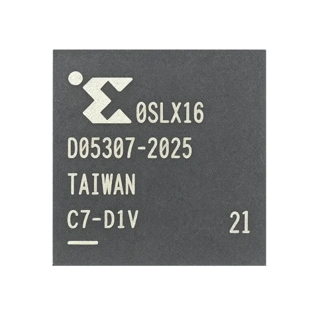
XC6SLX16-2CPG196I - 14k Logic Cells Spartan-6 FPGA | AMD
The AMD (Xilinx) XC6SLX16-2CPG196I is a Spartan-6 LX FPGA built on a 45 nm CMOS process, delivering 14,579 logic cells with 106 user I/Os in a 196-ball 8 mm × 8 mm CSBGA (TFBGA) package, with 576 Kbit of embedded block RAM and integrated DSP slices. The “-2” speed grade and industrial-grade (-40 °C to +100 °C) “I” temperature suffix indicate a -2 speed/performance tier intended for industrial-temperature environments. A Field Programmable Gate Array (FPGA) is a semiconductor integrated circuit built from configurable logic blocks (CLBs), programmable routing, and dedicated hardware resources such as block RAM, multipliers/DSP slices, and clock management tiles (DCMs/PLLs). The Spartan-6 LX series sits in the low-power, low-cost tier of the AMD/Xilinx product hierarchy: FPGA -> programmable logic -> logic IC -> integrated circuit. Spartan-6 LX devices target high-volume, cost-sensitive bridging, control, and signal-processing applications that need the parallelism and reconfigurability of an FPGA without the cost of a Virtex-class device. Key features of the XC6SLX16-2CPG196I include: 14,579 logic cells (~2,300 logic slices), 106 maximum user I/Os (some version/board use this number; package allows up to 106), 576 Kbit (72 Kbyte) of block RAM, 32 DSP48A1 slices, four DCMs and two PLLs for clock management, on-chip memory controllers (MCB) for DDR/DDR2/LPDDR, and a 1.2 V core supply with dedicated high-performance/low-power transceiverless I/O banks. The device is implemented on 45 nm process technology, delivering low static and dynamic power versus previous Spartan generations. The -2 speed grade is the mid-tier in the Spartan-6 family and balances Fmax and power for typical industrial designs. Architecturally, the XC6SLX16-2CPG196I uses a register-rich, columnar LUT-6 architecture with dedicated carry chains, distributed RAM/SRL16 shift-register logic in each CLB, and a hard PCIe endpoint block on higher-density siblings (note: LX16 does not include the integrated PCIe block; it is on LX45+). Multiple I/O standards (LVCMOS, LVDS, HSTL, SSTL) are supported with per-bank reference voltages, and the package is lead-free (Pb-free) RoHS-compliant. The 8 × 8 mm CSBGA package supports high-density board layouts in space-constrained designs. Typical applications include industrial motor control and factory automation, automotive infotainment displays and driver-assistance modules, consumer video bridging (HDMI/LVDS), low-cost software-defined radio front-ends, embedded vision pre-processing, and communication backplane bridging. The 576 Kbit of block RAM and 32 DSP slices make the LX16 well suited to small FIR/IIR filters, modest FFT engines, sensor-fusion pre-processing, and glue-logic aggregation. Pairing with a small external SPI flash for configuration memory keeps the BOM lean. When designing with this FPGA, verify that the -2 speed grade meets your target Fmax for the design floorplan, ensure JTAG and DONE pull-up values match the Spartan-6 configuration user guide, and check I/O-bank voltage compatibility before mixing 3.3 V peripherals with 1.2 V core logic. Note: the LX16 does not include the integrated PCIe block; use LX45/LX75/LX100/LX150 if PCIe hard IP is required. This page synthesizes AMD/Xilinx datasheet specifications, distributor pricing as of 2026-10-11, same-package drop-in alternatives within the Spartan-6 family, and practical design notes.

XC6SLX16-2CSG225C - 14,579-LC Spartan-6 FPGA | AMD
The AMD XC6SLX16-2CSG225C is a Spartan-6 LX field-programmable gate array with 14,579 logic cells, 589,824 bits of block RAM, and 160 user I/O in a 225-ball CSPBGA package. The -2 device is built on 45 nm CMOS technology and operates from 0°C to +85°C. Its 225-LFBGA package measures approximately 19 mm by 19 mm with a 0.80 mm ball pitch and supports lead-free assembly. A field-programmable gate array, or FPGA, is a reconfigurable digital semiconductor used to implement logic, control, signal processing, and interface functions in programmable hardware. An FPGA belongs to the semiconductor hierarchy and combines configurable logic blocks, programmable I/O, memory resources, dedicated processing blocks, and clocking circuitry. The Spartan-6 LX family is positioned for cost-sensitive, high-volume systems that need more parallelism and performance than a basic microcontroller can provide. The XC6SLX16 combines 14,579 logic cells with 589,824 bits of block RAM and 160 I/O. Dedicated 18×18 multiplier resources support efficient digital signal processing, while cascade and pipelining features allow higher-performance arithmetic and filtering structures. Its programmable I/O and 45 nm architecture are useful for custom bridges, industrial interfaces, embedded control, video data processing, and communication equipment. The -2 suffix identifies the device's performance grade, while CSG225 specifies its 225-ball CSPBGA package. The C suffix identifies the commercial temperature grade. Verified distributor data reports a maximum internal frequency of 667 MHz, although achievable system performance depends on the selected design, timing constraints, I/O standards, clocking architecture, and memory interface configuration. Typical applications include industrial automation and factory control, machine vision, automotive infotainment, consumer video processing, embedded communications, and low-cost PCI-based systems. The 160 available I/O support integration with external memory, transceivers, sensors, displays, and industrial peripherals while the programmable fabric allows product revisions and field updates without changing the PCB. PCB design must follow AMD package, pinout, solder, and thermal guidance. The CSPBGA package requires careful escape routing, a suitable PCB land pattern, adequate power and ground distribution, and attention to via-in-pad or microvia fabrication requirements. Designers should use the published package files and the Spartan-6 configuration data rather than relying on generic BGA assumptions. This product page consolidates verified distributor specifications, lifecycle-relevant sourcing information, same-footprint Spartan-6 alternatives, comparison parameters, and practical implementation guidance. It also distinguishes documented facts from parameters that require confirmation in the complete AMD device documentation before layout or production release.
XC6SLX16-2CSG225I - Spartan-6 LX 14,579-Cell FPGA | AMD
The AMD Xilinx XC6SLX16-2CSG225I is a Spartan-6 LX field-programmable gate array (FPGA) with 14,579 logic cells, 1,139 configurable logic blocks, 24 hardware multipliers, and 144 I/O in a 225-LFBGA CSBGA package. The device is built on 45 nm CMOS technology, operates from a 1.2 V core supply, and is identified with an internal frequency of 667 MHz and a -2 speed grade. The XC6SLX16-2CSG225I also carries the industrial-temperature designation and is intended for cost-sensitive, high-volume embedded systems requiring a balanced combination of programmable logic, DSP resources, and I/O flexibility. A field-programmable gate array is a reconfigurable digital semiconductor in which the logic architecture and interconnect are defined after manufacture. Within the broader semiconductor hierarchy, this FPGA belongs to the programmable-logic device class, combines lookup-table-based combinational logic with programmable routing, and provides deterministic parallel processing for control, acquisition, communications, and signal-processing functions. The Spartan-6 LX family is positioned between fixed-function controllers and larger high-performance FPGAs. The XC6SLX16-2CSG225I provides 14,579 logic cells distributed across 1,139 CLBs, along with 24 dedicated multipliers for DSP-oriented arithmetic. Its 144 I/O support integration with external memory, converters, communication transceivers, and industrial interfaces. The 45 nm CMOS implementation supports a 1.2 V operating supply, while the -2 suffix identifies the device speed grade. The exact I/O standards, memory interface capacity, configuration data rates, and static-power limits are not present in the supplied verified records. The 225-LFBGA CSBGA package supports compact, high-density PCB integration but requires careful escape routing, via-in-pad or via-adjacent fanout, and controlled assembly-planar or ball-grid layouts. Because the verified package descriptions differ between 19 x 19 mm and 13 x 13 mm versions in secondary listings, the package dimensions should be checked against the authoritative AMD package drawing before layout release. The supplied comparison data identifies the target as a 225-pin package and also references a 484-pin listing that does not match the MPN designation. Typical uses include industrial automation and motor control, machine-vision preprocessing, sensor acquisition, programmable control, industrial communications, and embedded signal processing. These applications benefit from parallel I/O, deterministic hardware multipliers, and reconfigurable logic that can be updated without changing the PCB. The -2 speed grade and industrial-grade ordering designation are appropriate selections when a design requires a cost-sensitive Spartan-6 LX implementation rather than a higher-density or higher-performance FPGA. Designers should reserve all power, ground, configuration, clock, and decoupling connections according to the AMD Spartan-6 pinout and PCB guidelines. The verified records identify 144 I/O but do not provide a complete numbered pin map, so the pinout is intentionally not presented here. Programming toolchain compatibility, supported I/O standards, absolute maximum ratings, and exact decoupling requirements must be confirmed in the official AMD documentation for the selected package and speed grade. This product record consolidates verified distributor, manufacturer-resource, and cross-reference findings with engineering-focused application guidance, explicit uncertainty markers, and same-footprint alternatives. It also distinguishes the target from package, speed-grade, and temperature-grade variants that are related components but not automatically interchangeable for every production program.
XC6SLX16-2CSG324C - 14,579-Cell Spartan-6 LX FPGA | AMD
AMD XC6SLX16-2CSG324C is a Spartan-6 LX field-programmable gate array built on a 45 nm process, with 14,579 FPGA cells, 232 I/Os, a -2 speed grade, and a 324-LFBGA package. The device combines programmable logic, block RAM, and DSP resources in a single integrated circuit for compact digital control, signal-processing, communications, and industrial automation designs. Its stated internal frequency is 667 MHz, while its nominal supply voltage is 1.2 V. A field-programmable gate array, or FPGA, is a reconfigurable semiconductor that lets engineers implement digital logic functions through programmable configuration rather than a fixed mask set. Within the broader semiconductor hierarchy, an FPGA is a programmable digital logic device that sits alongside microcontrollers, DSPs, and ASICs. It is useful when a design needs parallel hardware, adaptable interfaces, or logic that can be updated after manufacture. The Spartan-6 LX family combines configurable logic blocks with dedicated block RAM and DSP48 processing resources. The verified product listing identifies 232 I/Os and 14,579 cells, providing a substantial logic surface for control planes, data acquisition, protocol bridges, and embedded signal-processing functions. The -2 suffix denotes the device speed grade, while the CSG324 ordering code identifies the specific 324-ball package variant used by the manufacturer. The supplied data describes the device as a lead-free 19 mm by 19 mm package with 0.80 mm pitch. One retrieved specification identifies the physical description as CSBGA-484, while the distributor listing identifies the orderable package as 324-LFBGA/CSPBGA; these package descriptions require confirmation against the official ordering information before footprint release. The stated operating temperature range is 0°C to 85°C for the version described by the retrieved datasheet source. Typical applications include industrial automation, bridging, communications, consumer equipment, and control systems where programmable logic and parallel I/O are valuable. An FPGA can implement multiple interfaces concurrently, while its configurable architecture allows design revisions without changing the physical device. Compared with a fixed-function ASIC, this flexibility is useful for prototypes and evolving systems, although FPGA power, clocking, and configuration requirements must be considered during design. A key design consideration is confirming the exact package, ball map, voltage requirements, configuration interface, memory resources, and I/O standards against the official AMD Spartan-6 documentation before layout or replacement qualification. This page consolidates verified distributor metadata, pricing references, package information, and drop-in replacement guidance while clearly identifying values that still require manufacturer confirmation. This information is intended for design comparison and sourcing support rather than certification. Spartan-6 LX devices in a common supported package may be pinout compatible, but engineers must verify the specific speed grade, temperature grade, device variant, package, and intended operating conditions before substitution.
XC6SLX16-2FT256C - 14,579-Cell Spartan-6 FPGA | AMD
The AMD XC6SLX16-2FT256C is a Spartan-6 LX field-programmable gate array with 14,579 configurable logic cells, 186 I/O, a 667 MHz internal frequency, and a 256-ball lead-free LBGA package. It uses 45 nm CMOS technology and a 1.2 V core supply, providing a compact programmable-logic platform for industrial, consumer, communications, and embedded-control systems. A field-programmable gate array is a semiconductor device whose digital logic, interconnect, and I/O behavior are configured after manufacture. In the product hierarchy, an FPGA sits above programmable logic devices and combines configurable logic blocks, block RAM, dedicated arithmetic resources, programmable I/O, and embedded processors. This integration allows one package to replace multiple programmable logic devices and supporting discrete components while shortening development cycles. The verified specifications identify 14,579 configurable cells, 1,139 CLBs, 186 I/O, a 667 MHz internal frequency, and 45 nm CMOS fabrication. The -2 suffix identifies the middle Spartan-6 LX speed grade, while C identifies the commercial temperature grade. These resources support parallel data processing, control-plane logic, communication bridges, signal conditioning, and general-purpose embedded systems without requiring a mask change for each design. As an FPGA, the XC6SLX16-2FT256C combines programmable digital logic with fixed physical resources. Its 186 I/O provide external connectivity, while the 256-ball surface-mount package supports compact board layouts. The 45 nm process and 1.2 V core supply place the device in a mature, low-power programmable-logic architecture intended for cost-sensitive designs that require more integration than discrete logic but less complexity than a large FPGA. Typical applications include industrial automation, industrial networking, video and image processing, consumer equipment, communications infrastructure, and embedded control. The Spartan-6 LX family is specifically identified as suitable for advanced bridging applications, automotive infotainment, consumer products, and industrial automation. A board using this device also requires a suitable configuration memory or boot interface, compliant power rails, clocking, decoupling, and careful signal-integrity routing. Designers should verify the exact FT256 pinout, supported I/O standards, configuration method, power-supply sequencing, and startup behavior in the AMD package files before layout release. Because the verified data does not provide the complete 256-ball pin map, no pin names should be inferred from generic BGA numbering. Differential interfaces should be routed with controlled length and impedance, while FPGA power and ground pins should follow the manufacturer's published connectivity and plane guidance. This product page consolidates distributor availability, package information, speed-grade variants, and practical replacement guidance in one engineering-focused reference. It also distinguishes true FT256 pin-compatible alternatives from package-only equivalents and clearly identifies specifications that require confirmation from the AMD Spartan-6 documentation.
XC6SLX16-2FT256I - Spartan-6 LX FPGA, 14K LCs, 256-BGA | AMD
The AMD (formerly Xilinx) XC6SLX16-2FT256I is a Spartan-6 LX family Field Programmable Gate Array (FPGA) with 14,579 logic cells, 589,824 bits of block RAM, and 186 user I/O, housed in a 256-ball Fine-Pitch Thin Ball Grid Array (FTBGA-256) package with industrial-grade -40C to +100C temperature rating and -2 speed grade performance. An FPGA (Field Programmable Gate Array) is a semiconductor integrated circuit composed of configurable logic blocks (CLBs), programmable interconnect, and dedicated silicon IP such as block RAM, DSP slices, and clock management tiles (CMTs). FPGAs occupy a position between general-purpose microcontrollers (software-defined behavior, sequential execution) and application-specific integrated circuits (ASICs, fixed function, highest performance per watt). The Spartan-6 family specifically targets cost-sensitive, high-volume applications where ASIC NRE costs are prohibitive but microcontroller performance is insufficient. Key features of the XC6SLX16-2FT256I include 2,278 Kbits total block RAM, 32 DSP48A1 slices for fixed-point and signal-processing arithmetic, four clock management tiles (CMTs) with digital clock managers (DCMs) and phase-locked loops (PLLs), and integrated SelectIO technology supporting single-ended and differential I/O standards up to 1080 Mbps. The device is fabricated on a 45 nm CMOS process and operates from a 1.2 V core supply with separate I/O bank voltages from 1.2 V to 3.3 V. Architecturally, the Spartan-6 LX family uses a 6-input LUT-based logic fabric with dedicated carry chains, distributed SRL16/SRL32 shift-register primitives, and a 16-bit block RAM/FIFO controller per BRAM tile. The 256-ball FTBGA package provides 186 effective user I/O after accounting for power, ground, configuration, and dedicated JTAG pins. Typical applications include industrial motor control, video processing pipelines, low-cost software-defined radio, LED video wall controllers, and embedded vision pre-processing. The 256-BGA package suits designs requiring dense I/O and moderate thermal dissipation. When designing with this device, ensure proper decoupling with 100 nF ceramic capacitors at every supply pin and a 4.7-10 uF bulk capacitor near the core rail. Configuration can be sourced from SPI flash, JTAG, or BPI parallel memory; the dedicated DONE and INIT_B pins must be monitored for proper startup sequencing. This page synthesizes distributor pricing, verified drop-in alternatives, and practical design notes not found in the manufacturer datasheet alone.