Interface ICs
Subcategories
Products (3,400+)

SN65HVD70DGSR - 3.3V Full-Duplex RS-485 400kbps Transceiver, 10-VSSOP | Texas Instruments
The Texas Instruments SN65HVD70DGSR is a 3.3 V, full-duplex RS-485 transceiver rated for data rates up to 400 kbps, integrating ±12 kV IEC 61000-4-2 contact discharge ESD protection, in a 10-pin VSSOP (DGS) PowerPAD package. The device pairs one differential driver with one differential receiver, each with dedicated input/output pins, enabling simultaneous transmit and receive on a four-wire bus typical of RS-422 and full-duplex RS-485 networks. The driver includes active-high enable control and the receiver includes active-low enable control, allowing a sub-5 µA standby current when both functions are disabled. A transceiver of this class is the physical-layer interface between a UART/MCU and a differential twisted-pair cable in industrial multipoint networks. The SN65HVD70 extends TI's RS-485 portfolio as a low-power, robust 3.3 V member of the SN65HVD7x family, suitable for half- and full-duplex links across factory floors, building automation, and motor-drive backplanes. As a line transceiver it sits hierarchically below the protocol layer (Modbus, PROFIBUS, DMX512) and above the cable plant, converting CMOS/TTL logic levels into the differential A/B signaling defined by TIA/EIA-485-A and TIA/EIA-422-B. Key features include ±30 kV HBM ESD on the bus pins, a wide 3.0 V to 3.6 V supply range, a 1.8 V to 5 V logic interface (no level shifter needed in 1.8 V systems), open-circuit, short-circuit, and bus-idle fail-safe receiver inputs, and a thermal-shutdown protected driver. The 10-pin VSSOP package with thermal pad keeps the footprint compact while supporting industrial -40 °C to +125 °C operation. The device uses a precision differential architecture with large receiver hysteresis (typically 50 mV) to reject common-mode noise on long cable runs. The wide common-mode range of -7 V to +12 V tolerates ground potential differences between nodes, and the 1/8 unit-load option permits up to 256 nodes on a single bus. Slew-rate limiting reduces EMI reflections on unterminated stubs. Typical applications include industrial multi-drop RS-485 networks, building-automation backbones, motor-control command links, point-of-sale peripherals, and full-duplex RS-422 point-to-point data links. The device is well matched to long cable runs with proper 120 Ω termination at both ends. When designing with this part, place 100 nF decoupling capacitors within 2 mm of VCC and use a 120 Ω termination resistor at each end of the bus. Do not leave unused driver outputs floating - tie them to GND through a resistor. Maintain a 1/8 unit-load budget when scaling beyond 32 nodes. This page synthesizes distributor pricing, drop-in alternatives, and practical design notes not found in the manufacturer datasheet, including cross-vendor equivalents and full intent coverage in the FAQ for engineers planning second-source qualification.

SN65HVD71D - 400kbps Full-Duplex RS-485 Transceiver | Texas Instruments
Texas Instruments SN65HVD71D is a 3.3 V full-duplex RS-485 and RS-422 transceiver with one driver and one receiver, a 400 kbps data rate, and 12 kV IEC ESD protection. It is packaged in an 8-pin SOIC (D) package and operates without driver or receiver enable controls. The separate driver input and receiver output pins support simultaneous bidirectional communication on a multidrop industrial bus. An RS-485 transceiver is an interface integrated circuit that converts logic-level signals into differential bus signals and converts received differential signals back into CMOS-compatible logic. RS-485 extends communication distance and noise immunity compared with single-ended interfaces by using balanced differential signaling. This family belongs to the interface IC hierarchy: transceiver > RS-485 interface > differential bus interface > semiconductor. The SN65HVD71D provides a 3.3 V supply range of 3 V to 3.6 V, operation from -40 °C to +125 °C, and a data rate up to 400 kbps. Its 12 kV IEC-rated ESD protection helps protect the transceiver when cables are connected to external equipment. Full-duplex operation allows transmitting and receiving simultaneously, which is useful for point-to-point links and systems that cannot wait for a bus turnaround. Internally, the device combines one differential driver and one differential receiver. The driver accepts a CMOS-compatible transmit input, while the receiver produces a CMOS-compatible receive output. The absence of enable pins simplifies control logic, although the design must manage bus direction externally when the transceiver is connected to a shared multidrop network. Typical applications include industrial RS-485 links, building automation, factory equipment, motor-control systems, security equipment, and other long-distance serial networks. The device can also support point-to-point RS-422-style connections when the system requires independent transmit and receive paths. Designers should check the pin assignment and termination requirements in the manufacturer datasheet before layout. A 120-ohm termination resistor is commonly used at each end of a standard RS-485 bus, while bias resistors should be placed only where required. Keep the differential pair routed together, minimize stubs, and provide a stable return path to reduce common-mode noise. This product page combines the manufacturer's electrical specifications with practical interface guidance, application context, comparison information, and verified sourcing references. It is intended to help engineers identify whether the SN65HVD71D fits a 3.3 V full-duplex RS-485 design before beginning PCB implementation.
SN65HVD72D - 3.3V 250kbps Half-Duplex RS-485 | Texas Instruments
The Texas Instruments SN65HVD72D is a 3.3 V half-duplex RS-485 transceiver with IEC ESD protection and a maximum signaling rate of 250 kbps, packaged in an 8-pin SOIC (D) package. It combines one RS-485 driver and one RS-485 receiver in a single integrated circuit, making it suitable for bidirectional industrial communication links using differential bus wiring. The part is identified by Texas Instruments as an active product with an operating temperature range of -40 °C to 125 °C and RoHS-compliant construction. An RS-485 transceiver is an interface IC that translates between a logic-level UART or digital signal and a differential RS-485 bus. The differential architecture supports noise-resistant communication over longer cable runs than single-ended signaling, while the half-duplex arrangement allows the same pair of bus conductors to support both transmission and reception. In this device, the 3.3 V supply and 250 kbps data rate suit embedded systems, industrial controllers, sensors, and equipment using low-speed field-bus links. Key verified characteristics include a 3.3 V supply, 250 kbps maximum signaling rate, half-duplex operation, RS-422/RS-485 transceiver functionality, and IEC ESD protection. The SOIC-8 package provides a compact surface-mount footprint for industrial control boards and communication modules. The device is marketed for demanding industrial applications where robust bus interfacing and protection are important. The SN65HVD72D integrates the physical-layer functions needed to connect a microcontroller or programmable logic controller to a differential RS-485 network. Designers should pay attention to bus biasing, termination, grounding, cable length, and the exact logic-control requirements of the selected family variant. The manufacturer product page and part-details page are the authoritative sources for ordering information, electrical characteristics, and package details. Typical uses include industrial automation equipment, remote sensor interfaces, building-control systems, instrumentation, and embedded serial networks. Compared with lower-speed or more highly integrated interface solutions, the SN65HVD72D provides a focused 250 kbps half-duplex RS-485 solution with ESD protection in a standard 8-pin SOIC package. This page combines verified manufacturer and distributor information with practical selection guidance, pricing context, and application notes for engineers evaluating the SN65HVD72D.

SN65HVD73D - 20Mbps Full-Duplex RS-485 | TI
The Texas Instruments SN65HVD73D is a 3.3 V full-duplex RS-485/RS-422 transceiver with a 20 Mbps maximum data rate, ±12 kV IEC ESD protection, and individual driver and receiver enables in a 14-pin SOIC (D) package. The device integrates one driver and one receiver, supports a 3 V to 3.6 V supply range, operates across -40°C to +125°C, and provides 70 mV receiver hysteresis. An RS-485 transceiver is a physical-layer interface IC that converts low-voltage digital logic signals into differential bus signals and reconstructs logic-level data from a differential bus. It belongs to the transceiver hierarchy within interface ICs and enables robust, point-to-point or multidrop communication over longer distances than single-ended logic interfaces. Full duplex means the driver and receiver can operate simultaneously on separate differential pairs. The SN65HVD73D's principal features include a 20 Mbps data rate, 70 mV receiver hysteresis, separate active-high driver enable and active-low receiver enable controls, and ±12 kV IEC-rated ESD protection. Its 3 V to 3.6 V operating range is appropriate for 3.3 V systems. The broad -40°C to +125°C temperature range supports industrial and extended-temperature equipment when the complete system qualification permits it. The integrated driver and receiver provide one RS-485/RS-422 communication channel in full-duplex configuration. Separate enables allow the transmitter and receiver to be disabled independently, and the manufacturer product page states that standby current can be reduced below 5 µA when both functions are disabled. A common ground reference and carefully terminated differential wiring remain necessary for reliable operation. Typical applications include industrial control networks, factory automation equipment, data acquisition systems, building-automation controllers, and communications between a host controller and a peripheral transceiver. The 20 Mbps capability supports high-speed point-to-point links, while the ±12 kV IEC ESD rating helps protect external bus connectors in electrically noisy environments. Designers should follow the manufacturer datasheet for transceiver pinout, termination, fail-safe biasing, and differential routing. Keep the RS-485 differential pair routed as a controlled-impedance pair, minimize stub lengths, place termination only where required by the bus topology, and verify grounding and surge-protection requirements for the installed environment. This product summary consolidates verified manufacturer and distributor information, supply parameters, design guidance, and replacement constraints into one engineering-focused reference. It also clearly distinguishes verified specifications from electrical values that require confirmation from the complete datasheet before schematic release.
SN65HVD73DGS - 3.3V Full-Duplex RS-485 20Mbps | Texas Instruments
The Texas Instruments SN65HVD73DGS is a 3.3 V full-duplex RS-485 transceiver with integrated active-high driver enable and active-low receiver enable pins, supporting data rates up to 20 Mbps in a 10-pin VSSOP (DGS) package. It integrates a differential driver, a differential receiver, and 12 kV IEC ESD protection on bus pins, operating from a single 3.3 V supply across the industrial -40°C to +125°C temperature range. The device is designed for high-speed, half-duplex-to-full-duplex RS-485 networks in industrial automation, motor control, and point-to-point data links. A RS-485 transceiver is a balanced differential line driver/receiver IC that converts a single-ended TTL/CMOS logic signal into a differential signal conforming to the TIA/EIA-485-A standard, enabling robust multi-drop communication over twisted-pair cable with common-mode voltage tolerance up to ±25 V and cable lengths up to 1200 m at reduced data rates. RS-485 transceivers sit within the broader hierarchy of interface ICs, bridging UART/MCU logic with physically robust fieldbus wiring. The SN65HVD73DGS belongs to the 3.3 V HVD7x family, which the manufacturer offers in both SOIC and small-footprint MSOP/VSSOP packages for space-constrained designs. Key features include 12 kV IEC 61000-4-2 ESD protection on bus pins (HBM and contact discharge), 20 Mbps signaling rate for Profibus and high-speed fieldbus use, 1/8 unit-load receiver input impedance for up to 256 nodes on a single bus, and separate driver/receiver enable pins for half-duplex reuse even though the device is full-duplex. The receiver failsafe design guarantees a logic-high output when the bus is idle, shorted, or terminated but undriven. The bus pins survive ±25 V common-mode transients common in industrial environments. Architecturally, the SN65HVD73DGS uses a 3.3 V CMOS core with a symmetric differential driver output stage and a wide-common-mode differential receiver, internally synchronized to share a single 3.3 V supply rail. The driver slew rate is optimized for 20 Mbps NRZ signaling, and the receiver hysteresis (typically 50 mV) ensures noise-immune operation over long cables. Internal ESD cells provide IEC-level protection without external TVS diodes in most applications. Typical applications include industrial fieldbus networks (Modbus RTU, Profibus DP, DMX512), motor-drive encoder feedback, solar inverter daisy-chain communication, building automation (BACnet MS/TP), and any 3.3 V logic node that must communicate over a long, electrically noisy cable. Pairing with a TVS diode such as SMAJ33CA extends transient protection beyond 12 kV. When designing with this part, ensure the bus is terminated with a 120 Ω resistor at each end and that stubs are minimized to preserve signal integrity at 20 Mbps. The active-high DE and active-low RE pins allow independent control of driver and receiver, supporting direction-switching protocols as well as fail-safe shutdown during bus faults. Decouple VCC with a 0.1 µF ceramic capacitor placed within 5 mm of the supply pin.
SN65HVD73DGSR - 3.3V Full-Duplex RS-485, 20Mbps, 12kV ESD | TI
The Texas Instruments SN65HVD73DGSR is a 3.3-V full-duplex RS-485 transceiver with separate driver and receiver pins, 20 Mbps signaling rate, and ±12-kV IEC 61000-4-2 contact ESD protection, housed in a 10-pin MSOP/VSSOP (DGS) package. The wide common-mode voltage range makes the device suitable for multi-point RS-485 / RS-422 bus applications over long cable runs in industrial, building automation, and motor-control networks. A RS-485 transceiver is a physical-layer interface IC that converts between a low-voltage UART/logic-level signal on the controller side and a balanced differential signal on the bus side. Full-duplex (a.k.a. 4-wire RS-485) uses separate differential pairs for transmit and receive, allowing simultaneous two-way communication. The SN65HVD73 belongs to the broader family of half- and full-duplex RS-485 transceivers -> differential line transceivers -> interface ICs -> integrated circuits in the data-communication hierarchy defined by TIA-485 / EIA-422 standards. Key features include 3.3-V single-supply operation (compatible with modern low-power MCUs and FPGAs), 20 Mbps maximum data rate, ±30-kV HBM and ±12-kV IEC 61000-4-2 contact-discharge ESD on bus pins, large receiver hysteresis for noise immunity in harsh industrial environments, 1/8 unit-load support that lets up to 256 nodes share one bus, and separate driver-enable (DE) and receiver-enable (RE) pins for direction control and half-duplex reuse. Operating temperature spans -40 °C to +125 °C. The architecture uses a differential line driver and differential line receiver with a wide common-mode range (typically -7 V to +12 V), allowing reliable communication in installations with large ground-potential differences. Internal slew-rate control and low bus-current loading support PROFIBUS, DMX512, and similar multi-drop protocols at 20 Mbps without external components. Typical applications include industrial field-bus nodes, motor encoder feedback links, building-automation gateways, solar inverter monitoring, and point-to-point backplane links between 3.3-V controllers. The wide common-mode range and IEC-grade ESD simplify compliance with industrial EMC requirements without external TVS arrays. When designing with this device, place the 100 nF VCC bypass capacitor as close to pin 10 as possible and use 120 Ω termination only at the two physical ends of the bus. Leave the middle of the bus unterminated to avoid loading reflections. The DE and RE pins let the host power-gate the part in sleep-mode designs by de-asserting both enables. This page synthesizes distributor pricing, drop-in alternatives from the TI SN65HVD7x family and cross-brand RS-485 ICs in the VSSOP-10 footprint, and practical design notes not found in the manufacturer datasheet alone.
SN65HVD74D - 3.3V 20Mbps Full-Duplex RS-485 | TI
The Texas Instruments SN65HVD74D is a 3.3 V full-duplex RS-485 transceiver with a 20 Mbps data rate, 12 kV IEC ESD protection, and an 8-pin SOIC package. It combines one differential driver and one differential receiver, providing separate data paths for simultaneous bidirectional communication over an RS-485 bus. The device supports a 3.0 V to 3.6 V supply range and operates from -40°C to 125°C. A transceiver interface IC converts between digital logic signals and balanced differential bus signals. The SN65HVD74 belongs to the RS-485 transceiver category within interface ICs, interface semiconductors, and broader communication semiconductors. Its differential signaling improves noise immunity by comparing the voltage between two bus conductors rather than referencing one conductor to ground, making it suitable for industrial, building-automation, and communications equipment operating over longer cable runs. The SN65HVD74D combines a 20 Mbps maximum data rate with more than 30 kV HBM ESD protection and more than 12 kV IEC61000-4-2 contact-discharge protection. Receiver hysteresis is 70 mV, helping reject conducted differential noise and prevent unwanted output transitions. Separate driver and receiver input and output pins support full-duplex bus arrangements without sharing a single half-duplex direction-control path. The transceiver operates from a single 3.3 V power supply and supports both RS-485 and RS-422 interface applications. Its surface-mount SOIC package permits automated assembly, while the stated -40°C to 125°C operating range supports industrial equipment, data-acquisition systems, factory controls, and industrial communication equipment. Each driver and receiver has separate input and output pins, allowing transmit and receive paths to operate simultaneously. Typical applications include full-duplex RS-485 industrial networks, high-speed instrumentation links, factory automation equipment, building-control systems, and industrial data acquisition. In a typical circuit, the microcontroller-facing pins connect to digital logic, while the differential A, B, Y, and Z pins connect to the balanced bus through suitable termination and protection components. The 70 mV receiver hysteresis helps maintain reliable decisions in electrically noisy environments. When designing the interface, maintain compatible logic levels, observe recommended bus biasing and termination, and verify that the selected cable length and topology remain valid for 20 Mbps operation. Protection-device capacitance should be included when calculating edge rate and channel performance. The 3.3 V supply must remain within the specified 3.0 V to 3.6 V range, and system designers should check all logic thresholds against their controlling device. This page combines the manufacturer's key electrical and environmental ratings with practical interface-design guidance, packaging information, and a focused drop-in replacement assessment. It highlights where the SN65HVD74D fits within a 3.3 V full-duplex RS-485 design and the checks that matter when evaluating bus speed, ESD robustness, receiver noise immunity, and PCB implementation.
SN65HVD75D - 3.3V 20Mbps RS-485 Transceiver | Texas Instruments
Texas Instruments SN65HVD75D is a 3.3 V half-duplex RS-485 transceiver with IEC ESD protection and a maximum signaling rate of 20 Mbps, housed in an 8-pin SOIC package. It supports operation from -40°C to 125°C and accepts 5 V-tolerant logic inputs compatible with 3.3 V or 5 V controllers. An RS-485 transceiver is an interface IC that combines a differential line driver and differential receiver, allowing digital data to be transmitted reliably over balanced, multipoint communication buses. The SN65HVD75 belongs to the transceiver hierarchy of interface ICs, differential line-driver and receiver circuits, and industrial communication semiconductors. Its half-duplex configuration permits a shared pair of conductors to carry data in either direction, but only one direction at a time. The SN65HVD75D operates from a 3.3 V supply, reaches 20 Mbps, and provides IEC ESD protection on the bus pins. Its logic interface supports 3.3 V and 5 V controllers, which simplifies connection to mixed-voltage digital systems. The wide -40°C to 125°C temperature range also makes the device suitable for industrial environments where commercial-temperature interface ICs may be inadequate. Exact ESD ratings, receiver thresholds, and electrical limits must be confirmed in the manufacturer datasheet. Each device combines a differential driver and differential receiver operating from one 3.3 V power supply. The bus pins are designed for robust ESD-event handling, including Human Body Model and IEC Contact Discharge protection. The manufacturer datasheet also identifies 250 kbps, 20 Mbps, and 50 Mbps signaling-rate options across the SN65HVD7x family, with 20 Mbps specifically associated with the SN65HVD75. Typical uses include industrial automation controllers, factory data buses, industrial instrumentation, building automation, and communications equipment operating on RS-485 networks. Its 20 Mbps capability supports high-speed half-duplex links, while 5 V-tolerant logic inputs ease interfacing with both 3.3 V and 5 V controllers. The half-duplex arrangement also requires careful direction-control design because the driver and receiver share the same bus pair. When designing the circuit, place a 100 nF ceramic bypass capacitor close to the supply pins and use a 3.3 V source capable of supporting the transceiver's operating current. The manufacturer recommends the TPS76333 for a suitable 3.3 V supply and the SN6501 for isolated power-supply designs. Bus routing should minimize stubs and maintain controlled differential impedance. This page combines verified manufacturer and distributor information, transparent pricing-status notes, same-family replacement analysis, and practical RS-485 design guidance. It also distinguishes verified electrical facts from parameters that still require confirmation against the complete SN65HVD7x manufacturer datasheet.
SN65HVD76D - 50Mbps Full-Duplex RS-485 | Texas Instruments
Texas Instruments SN65HVD76D is a 3.3 V full-duplex RS-485 transceiver with a 50 Mbps data rate, separate driver and receiver enables, and 12 kV IEC contact-discharge ESD protection. It is packaged as a 14-pin SOIC for surface-mount industrial and instrumentation systems. An RS-485 transceiver combines a differential line driver and differential receiver to communicate reliably over noisy, long-distance industrial buses. The SN65HVD76 family supports both RS-485 and RS-422 applications, while its full-duplex architecture provides simultaneous transmit and receive paths through separate differential pins. It operates from a single 3.3 V power rail, simplifying integration with 3.3 V controllers, sensors, gateways, and test equipment. The principal features include a 50 Mbps maximum data rate, 1/8 unit-load receiver operation for up to 256 nodes, a 70 mV receiver hysteresis, and separate enable controls. According to the Texas Instruments product page, the driver enable is active high and the receiver enable is active low. Disabling both functions can reduce standby current to less than 5 uA, making the device useful in low-power distributed systems. Bus protection includes greater than 30 kV human-body-model protection and greater than 12 kV IEC 61000-4-2 contact-discharge protection, together with greater than 4 kV IEC 61000-4-4 fast-transient burst protection. These ratings help protect the transceiver in electrically noisy environments, although they do not eliminate the need for correct common-mode grounding, cable selection, and termination practices. Typical applications include industrial RS-485 links, factory automation equipment, building controls, instrumentation, and high-speed data acquisition. Full-duplex operation is particularly appropriate when continuous receiving is required while the controller also transmits status, configuration, or diagnostic data. The 14-pin SOIC format also supports conventional surface-mount assembly and thermal design. For a new layout, place the transceiver and its protection or bypass components near the bus connector, maintain a continuous ground reference with the cable, and apply termination only where required by the network topology. Verify that the selected logic controller can tolerate the receiver output levels and that the bus does not exceed the device's electrical limits. This page combines the exact device specifications, practical RS-485 design guidance, application fit, and package-level comparison information. It also distinguishes true board-level drop-in options from related family members whose enable behavior or transceiver configuration differs, helping engineers avoid selecting a substitute that requires schematic or layout changes.
SN65HVD77D - 3.3V 50Mbps Full-Duplex RS-485 | Texas Instruments
Texas Instruments SN65HVD77D is a 3.3 V full-duplex RS-485 transceiver with a 50 Mbps data rate, ±12 kV IEC ESD protection, and an 8-pin SOIC package. It combines one differential driver and one differential receiver in a single package, allowing transmit and receive paths to operate simultaneously. The device operates from 3.0 V to 3.6 V and is specified across -40°C to 125°C. An RS-485 transceiver is an interface IC that converts logic-level signals into differential bus signals and converts received differential signals back into logic levels. RS-485 belongs to the differential data-interface hierarchy, where the voltage between the A and Y conductors carries the signal while common-mode noise is rejected. The SN65HVD77D is designed for robust, point-to-point, multidrop, and full-duplex industrial communication links. The primary feature of the SN65HVD77D is its 50 Mbps signaling capability, making it suitable for high-speed data acquisition, factory automation, industrial control, and communications equipment. Its ±12 kV IEC-rated ESD protection improves system resilience when cables connect the transceiver to external equipment. Operating from a 3.3 V rail also simplifies integration with 3.3 V controllers, FPGAs, DSPs, and other digital logic. Each device contains separate driver and receiver inputs and outputs, eliminating the shared bus direction controls commonly found on half-duplex transceivers. Full-duplex operation allows data to be transmitted and received at the same time. The transmitter drives a differential pair, while the receiver provides a complementary logic-level output. Because there are no external enable controls, the device is intended for continuous enabled operation rather than controlled low-power bus shutdown. Typical implementations connect the logic-side data pins to a communications controller, connect the A and Y pins to a protected twisted-pair bus, and place the receiver output in the controller's receive path. Full-duplex systems use separate differential pairs for transmission and reception. The SOIC-8 package supports conventional surface-mount assembly and is suitable for industrial control boards, test equipment, motor-control systems, and embedded communications modules. The principal design consideration is signal integrity. High-speed differential routing requires controlled impedance, a continuous return path, minimized stubs, and proper termination at the bus endpoints. External protection may still be required for severe industrial transients because the integrated ESD rating addresses electrostatic discharge rather than every surge or lightning event. This product page combines the manufacturer's principal electrical and environmental specifications with same-package transceiver options, application guidance, and practical PCB-layout considerations. These engineering details help simplify device selection, footprint verification, and robust RS-485 implementation.
SN65HVD96D - 5 Mbps SymPol Transceiver | Texas Instruments
The Texas Instruments SN65HVD96D is a half-duplex, 1/1 SymPol transceiver operating from a single 5 V supply in an 8-pin SOIC package. It supports signaling up to 5 Mbps, communicates reliably on normal or reversed-wire bus lines, and uses a symmetric-polarity receiver with 100 mV hysteresis. These characteristics make it suitable for industrial point-to-point, multi-drop, and multi-point communication networks. A SymPol transceiver is a physically robust bus interface integrated circuit that combines a differential driver and differential receiver into one package. It belongs to the interface IC hierarchy, alongside RS-485 transceivers, but uses symmetric polarity rather than the conventional RS-485 differential signaling convention. The SN65HVD96 series is an upgrade path for RS-485 installations, although the devices are not protocol-compatible with existing RS-485 networks. Key electrical features include a 4.75 V to 5.25 V supply range, one transmitter and one receiver, 5 Mbps signaling, 100 mV receiver hysteresis, and support for reversed-wire connections. The symmetric-polarity receiver helps the device interpret bus states consistently when conductors are connected in reverse. The 8-pin SOIC package also saves board area compared with equivalent discrete driver and receiver implementations. TI specifies an industrial operating range from -40 °C to 85 °C, making the device suitable for industrial instrumentation, factory automation, and commercial equipment that operates outside extended automotive temperature limits. The SOIC outline supports conventional surface-mount assembly, while the eight-pin footprint reduces the number of components needed to implement a robust bus node. Typical uses include industrial sensor networks, process-control equipment, remote monitoring stations, PLC peripheral interfaces, and point-to-point data links between controllers and field devices. Because the SN65HVD96D supports reversed wiring and 5 Mbps signaling, it is particularly useful where field installation errors or shorter, higher-speed interconnects are expected. The device pinout is identical to the industry-standard SN75176 transceiver, allowing an SN75176-based board to be considered for a SymPol migration. Existing RS-485 firmware and system behavior are not automatically compatible because SymPol is not backward compatible with RS-485, so the bus protocol and termination strategy must be reviewed before replacement. This page consolidates verified manufacturer and distributor information, package and pinout details, application guidance, and migration considerations that are not presented together on a standard distributor listing. Pricing and drop-in replacement availability are reported only where supported by verified source data.
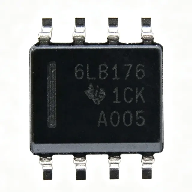
SN65LBC176DR - 10Mbps RS-485 Transceiver 5V | Texas Instruments
The Texas Instruments SN65LBC176DR is a differential bus transceiver combining a 3-state differential line driver and a differential input line receiver, both operating from a single 5V supply, in an 8-pin SOIC (D) package rated from -40C to +85C. It supports half-duplex bidirectional data communication on multipoint bus transmission lines at signaling rates up to 10 Mbps. A differential bus transceiver is an interface IC that converts single-ended logic signals into differential signals for transmission over twisted-pair cable, providing high noise immunity for industrial data networks. The SN65LBC176 belongs to the RS-485/RS-422 transceiver family within the broader hierarchy of interface ICs and line drivers, and it meets or exceeds the requirements of ANSI TIA/EIA-485 (RS-485) and ISO 8482:1987 (E). Key features include a driver enable (DE, active-high) and receiver enable (RE, active-low) that can be tied together to form a single direction-control pin, low-skew LinBiCMOS technology designed for high-speed serial and parallel data transmission, and bus fault protection across a -10V to +15V common-mode range. The driver outputs differential signals on pins A and B while the receiver accepts differential input, allowing direct connection to the multipoint bus. One driver and one receiver per device simplify point-to-point and multidrop network nodes. The LinBiCMOS process yields low power consumption with high output drive, supporting bus loading of up to 32 unit loads and cable lengths of several thousand feet at lower data rates. Typical applications include industrial automation networks, motor-drive communication links, building automation, energy metering, and any half-duplex RS-485 fieldbus requiring 10 Mbps throughput. Design tip: bias the bus with fail-safe resistor dividers (typically 560 ohm to the A-line pull-down and B-line pull-up) and terminate both bus ends with 120 ohm to prevent reflections and ensure a defined receiver state when all drivers are disabled.

SN65LVDS31D - 400 Mbps Quad LVDS Driver | Texas Instruments
The Texas Instruments SN65LVDS31D is a 400-Mbps low-voltage differential signaling (LVDS) quad high-speed differential driver with four independent driver outputs, a 3.3 V supply, and a 16-pin SOIC package. According to the manufacturer product data, it meets or exceeds ANSI TIA/EIA-644 requirements and provides a typical differential output voltage of 350 mV into a 100-ohm load. An LVDS differential line driver is a high-speed interface IC that converts CMOS or LVTTL inputs into low-voltage differential outputs. In the broader hierarchy, an LVDS driver belongs to differential line-driver ICs, interface ICs, and semiconductors. Its differential signaling reduces common-mode noise sensitivity and supports reliable point-to-point data transmission over balanced interconnects. Key features include four drivers in one package, operation from a 3.3 V supply, 400-Mbps signaling capability, typical 1.7 ns propagation delay, and typical output rise and fall times of 500 ps. The manufacturer product page also identifies pin compatibility with AM26LS31, MC3487, and µA9638, enabling board-level substitution where electrical and timing requirements are confirmed. The SN65LVDS31D is intended for high-speed point-to-point links, including display and video backplanes, industrial control links, communications equipment, and test systems. Differential outputs help maintain signal integrity when the source and destination are connected through controlled-impedance traces or a suitable cable. When designing around this device, use the manufacturer’s recommended termination and layout practices. Confirm trace impedance, keep the differential pair routed with matched geometry, provide adequate bypassing near the supply pins, and verify receiver, cable, and connector characteristics. The supplied data confirms -40°C to +85°C operation for the SOIC-16 device, while other electrical limits should be taken directly from the manufacturer datasheet. This page combines the verified manufacturer identification, distributor listing, pricing reference, interface context, and engineering-focused application guidance. It is intended to help engineers identify the correct part, validate compatibility, and plan a robust LVDS interconnect without treating unsupported parameters as guaranteed specifications.
SN65LVDS32D - 400 Mbps Quad LVDS Receiver | Texas Instruments
Texas Instruments SN65LVDS32D is a 400 Mbps quad high-speed differential receiver designed for low-voltage differential signaling (LVDS), supplied from a single 3.3 V supply and housed in a 16-pin SOIC package. It provides four differential receiver channels, differential input thresholds of 100 mV maximum, typical propagation delay of 2.1 ns, and typical power dissipation of 60 mW. The receiver is intended for systems requiring reliable high-speed differential input reception under industrial and automotive-qualified conditions. An LVDS receiver is an interface circuit that converts a small differential voltage across a balanced pair into a digital logic signal. It belongs to the receiver and transceiver interface IC category, within broader communication-interface and signal-conditioning electronics. Differential reception rejects common-mode noise and helps maintain signal integrity across longer interconnects or cables than ordinary single-ended logic receivers. The SN65LVDS32D implements the electrical characteristics associated with ANSI TIA/EIA-644, as identified in the manufacturer product data. Key features include four independent receiver channels, operation from one 3.3 V supply, signaling rates up to 400 Mbps, 100 mV maximum differential input threshold, and open-circuit fail-safe behavior suitable for cold-sparing and redundant systems. The manufacturer product page also identifies pin compatibility with AM26LS32, MC3486, and µA9637. Automotive qualification and ESD protection features make the device relevant to industrial control, communications, test equipment, and vehicle electronics where differential signaling is required. The electrical performance is centered on low-latency differential reception. A typical 2.1 ns propagation delay is useful when the system must preserve timing relationships across multiple channels. The 60 mW typical power dissipation provides a practical baseline for power budgeting, although actual dissipation depends on supply voltage, input activity, output loading, and operating temperature. The single-supply architecture simplifies system power design while requiring correct input common-mode and termination practices. Typical applications include industrial automation links, high-speed data acquisition, point-to-point communications, test and measurement equipment, and automotive or other harsh-environment interfaces. In these systems, the receiver is placed after a balanced transmission line and connected to downstream digital logic through its four differential receiver outputs. Designers should verify the complete channel budget, cable or PCB loss, termination, grounding, and input common-mode range in the system-level design. A key design consideration is preserving the LVDS signal path: use controlled-impedance routing, matched differential pair geometry, appropriate termination, and short return paths to avoid degrading the 400 Mbps target. Do not treat the receiver as a general-purpose comparator or add logic without checking the output timing, supply requirements, and pin-specific electrical limits. This page combines the verified manufacturer and distributor information with practical LVDS design guidance for component selection and implementation.

SN65LVDS93ADGGR - LVDS Serializer 10-135MHz 56-TSSOP | TI
The Texas Instruments SN65LVDS93ADGGR is a FlatLink LVDS serializer (SerDes transmitter) that converts 28 bits of single-ended LVTTL parallel data into 4 LVDS data pairs plus 1 LVDS clock pair, operating over a 10 MHz to 135 MHz input clock range in a 56-pin TSSOP (DGG) package rated from -40C to +85C. An LVDS (Low-Voltage Differential Signaling) serializer is an interface IC that compresses a wide parallel data bus onto a small number of high-speed differential pairs, dramatically reducing connector size, cable count, and EMI between a host processor and a display or backplane. Within the signal-chain hierarchy, it belongs to the SerDes (serializer/deserializer) family of high-speed interface products, sitting between parallel LVTTL logic and LVDS physical-layer line drivers. Key features of the SN65LVDS93A include 28:4 data channel compression delivering up to 1.904 Gbps serialized throughput per the datasheet, an integrated 7x clock synthesizer that multiplies the input reference clock, and five LVDS line drivers meeting the TIA/EIA-644 LVDS standard for low EMI differential signaling. The A-suffix version extends the supported operating range to 10 MHz - 135 MHz, making it faster than the base SN65LVDS93, which is specified from 20 MHz to 68 MHz on TI.com. Architecturally, the device contains four 7-bit parallel-load serial-out shift registers, the 7x PLL clock synthesizer, and five LVDS drivers in a single IC. Data is latched on the parallel clock, shifted out at 7x rate, and transmitted with the embedded clock pair so a matching deserializer such as the SN65LVDS96 or DS90CF384 can recover timing without a separate clock channel. LVDS current-mode drivers on a 3.3V supply produce approximately 350 mV differential swings with low skew. Typical applications include TFT-LCD panel interfacing in industrial displays and medical monitors, video transmission between a graphics controller and a FlatLink-compatible display, and point-to-point board-to-board links where a 28-bit parallel bus must cross a flex cable or backplane with minimal wiring. When designing with this device, keep the parallel input setup/hold times within datasheet limits and route the LVDS pairs as controlled-impedance 100-ohm differential traces; also confirm the exact input clock range against your system, since TI lists both a 10-135 MHz range (A version) and 20-68 MHz (base part) across product pages. This page synthesizes distributor inventory data, drop-in alternatives, pinout guidance, and practical design notes not found in the manufacturer datasheet alone, with pricing refreshed as of 2026-10-19.

SN65LVDT100DGK - 2Gbps LVDS Repeater/Translator | Texas Instruments
The Texas Instruments SN65LVDT100DGK is a 2-Gbps LVDS, LVPECL and CML to LVDS repeater/translator in an 8-pin VSSOP (DGK) package. It accepts low-voltage differential signaling (LVDS), positive-emitter-coupled logic (PECL), or current-mode logic (CML) input signals at signaling rates up to 2 Gbps and regenerates them as clean LVDS output levels, operating from a single 3 V to 3.6 V supply. A differential repeater/translator is an interface IC that sits in a high-speed serial signal path, receiving a degraded or logic-incompatible differential signal and re-driving it with fresh, standard-compliant output levels. Within the signal-chain hierarchy, it belongs to the buffer/repeater family of interface ICs, bridging logic families (LVDS, LVPECL, CML) that would otherwise require discrete level-shifting networks and termination circuitry. Key features include a maximum total jitter of 100 ps, low part-to-part skew, and receiver input threshold hysteresis of tens of millivolts for noise immunity on marginal input signals. A distinctive advantage is the integrated 110-ohm differential line termination resistor, which shortens stub length, reduces component count, and saves board space compared with discrete 100-ohm termination schemes. TI positions this device as a low-power alternative to the MC100EP16 ECL repeater. Architecturally, the receiver front-end accepts a wide-range differential input (LVDS, PECL, or CML swings) and drives a current-mode LVDS output stage designed for 100-ohm differential transmission lines. The short signal path through the device (analog repeat, no FIFO or retiming logic) keeps propagation delay low, and TI's Bipolar/high-speed process supports multi-gigabit signaling while remaining within a modest supply-current budget at 3.3 V. Typical applications include backplane and point-to-point LVDS link conditioning, clock distribution and repeating in telecom and networking equipment, and extending LVDS display or camera links where cable losses degrade eye diagrams. Where a PECL output is required instead of LVDS, the companion SN65LVDS100/SN65LVDT101 family members cover that case in related packages. Design consideration: keep the input traces to the integrated termination as short as possible; the device must receive a differential signal that crosses its threshold window with hysteresis, so check eye margins at 2 Gbps with your actual channel loss before committing to layout. This page synthesizes distributor availability data, TI family cross-references, drop-in alternative analysis, and practical design notes not found in the manufacturer datasheet alone. Pricing shown is as of 2026-10-19 and is an estimate pending live distributor verification.
SN65MLVD200ADR - Half-Duplex M-LVDS Transceiver, 8-SOIC | TI
The Texas Instruments SN65MLVD200ADR is a half-duplex Multipoint-LVDS (M-LVDS) transceiver in an 8-pin SOIC package, with one driver and one receiver sharing a single differential bus pair. It conforms to the M-LVDS standard (TIA/EIA-899) and supports data rates up to 100 Mbps (200 Mbps in some drive modes) with low 700 ps driver output skew, making it suitable for high-speed multipoint backplane and clock-distribution links. The IC operates from a single 3.3 V supply and provides 24 mA of drive current on the M-LVDS bus pins, with internal fail-safe biasing on the receiver inputs. Background: An LVDS (Low-Voltage Differential Signaling) transceiver is a type of high-speed differential interface IC that transmits data across a balanced pair of wires using low-swing, current-mode signaling, achieving high noise immunity at low power. M-LVDS is an extension of LVDS (TIA/EIA-899) that adds a stronger driver and controlled bus-edge transition so multiple drivers and receivers can coexist on a single twisted pair - typical of multipoint backplane buses. Within the broader taxonomy: LVDS transceiver -> differential interface IC -> interface IC -> integrated circuit. Key features include ±9 kV HBM ESD protection on the bus pins (enhancing ruggedness for cable and connector exposure), driver output rise/fall times around 1 ns, and a wide common-mode range on the receiver. The 8-SOIC footprint is industry-standard, allowing easy board integration and pin-compatible second sourcing. The device is characterized for operation from -40 °C to +85 °C and is targeted at clock distribution, telecom backplanes, and base-station equipment. Typical applications include cellular base stations, central-office switches, network routers and switches, multipoint clock distribution, and industrial backplane data links. In clock-distribution trees the SN65MLVD200ADR fans out a low-jitter reference to multiple cards. Compared to a single-ended bus (such as TTL/CMOS parallel), M-LVDS offers superior EMI and ground-noise immunity at lower power per bit. Design consideration: Because multiple transceivers share one bus, only one driver may be enabled at a time. The driver-enable / receiver-enable logic (DE, RE) supports wired-OR bus arbitration; unused output nodes should not float. Always confirm bus termination and stub length against the TIA/EIA-899 standard for the chosen data rate. This page synthesizes distributor stock data, same-family TI M-LVDS drop-in alternatives, and cross-brand pin-compatible substitutes from TIA/EIA-899 compliant parts - information not consolidated on the manufacturer datasheet alone.

SN74AUP1T34DCKR - 1-Bit Level Translator 0.9-3.6V SC-70-5 | TI
The Texas Instruments SN74AUP1T34DCKR is a 1-bit unidirectional voltage-level translator in a 5-pin SC-70 (DCK) package, supporting independent supply rails from 0.9 V to 3.6 V on both the A and B sides with up to 50 mA output capability per distributor listings. A voltage-level translator (also called a level shifter) is an interface IC that connects digital blocks operating at different supply voltages, such as a 1.8 V microcontroller GPIO driving a 3.3 V peripheral. Level translators belong to the interface IC family within the broader semiconductor hierarchy, sitting alongside bus switches, transceivers, and logic buffers. The SN74AUP1T34 is a fixed-direction, non-inverting single-channel device built on TI's Advanced Ultra-Low Power (AUP) process family. Key features include two separately configurable power rails (VCCA and VCCB can each be anywhere from 0.9 V to 3.6 V in any order), making it suitable for asymmetric translation such as 1.2 V to 3.3 V or 2.5 V to 1.8 V. The AUP architecture delivers very low dynamic power consumption and low static supply current, important for battery-powered and always-on designs. The device supports partial power-down operation via Ioff circuitry, so inputs and outputs remain high-impedance when either rail is unpowered, protecting downstream circuits during multi-rail sequencing. Technically, the translator combines a low-voltage input stage referenced to VCCA with a push-pull output stage referenced to VCCB, reproducing the input logic level on the output with correct CMOS levels on the destination rail. Because the direction is fixed (A to B) and the logic is non-inverting, it behaves like a buffer across domains and requires no direction-control pin, simplifying board design compared with bidirectional translators such as the TXB/TXS families. Typical applications include I2C-adjacent GPIO translation, UART and SPI signal buffering between voltage domains, enable/flag signal shifting in power-management circuits, and level adaptation in portable, wearable, and IoT boards where 1.2 V, 1.8 V, 2.5 V, and 3.3 V rails coexist. Design tip: keep both rails within 0.9 V to 3.6 V at all times and place 0.1 uF decoupling capacitors close to both VCCA and VCCB pins; note the SC-70-5 footprint is compact, so thermal and layout effort is minimal but probe access is limited. This page adds value beyond the TI datasheet by combining drop-in alternative cross-references, application guidance, and pricing comparison in one place.

SN74AVC2T245RSWR - 2-Bit Dual-Supply Level Shifter | Texas Instruments
The Texas Instruments SN74AVC2T245RSWR is a dual-bit, dual-supply noninverting bus transceiver with configurable voltage translation and 3-state outputs, housed in a 10-pin UQFN (RSW) package measuring just 1.8 mm x 1.4 mm. It operates from two independent supply rails (VCCA and VCCB) of 1.2 V to 3.6 V, enabling bidirectional logic-level translation between any two voltage domains. A dual-supply bus transceiver is a logic device that transfers data bidirectionally between two ICs operating at different logic levels, such as a 1.8 V microcontroller and a 3.3 V peripheral. It belongs to the broader hierarchy of voltage translators within interface logic ICs, and the SN74AVC2T245 is a member of TI's AVC (Advanced Very-low-voltage CMOS) family, optimized for high speed and low static power. Key features include independent direction control for each channel (DIR1 and DIR2), an output-enable (OE) pin for 3-state bus isolation, and a VCC isolation feature that forces all I/O ports to high impedance when either supply is at GND. The device achieves data rates up to 380 Mbps with a typical propagation delay of 2.4 ns and delivers 12 mA output drive at 3.3 V. The AVC architecture uses configurable level shifting: output levels are set automatically by VCCA and VCCB with no direction-strapping constraints. Ioff circuitry supports partial power-down operation by blocking backflow current when either rail collapses, and quiescent current is approximately 20 uA for battery-friendly designs. Typical applications include level shifting for I2C, SPI, UART, and GPIO buses in personal electronics, industrial control, and networking equipment. The 1.8 mm x 1.4 mm UQFN footprint suits space-constrained portable and wearable designs. Design consideration: keep both supplies within 1.2 V to 3.6 V at all times, and use the OE pin with a pull-down so the bus stays tri-stated during power-up to avoid contention.
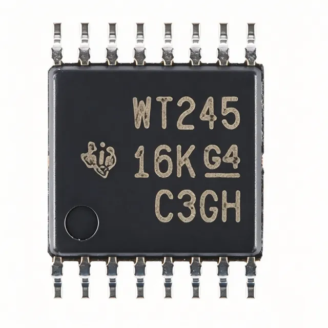
SN74AVC4T245PWR - 4-Bit Dual-Supply Level Shifter | TI
The Texas Instruments SN74AVC4T245PWR is a 4-bit dual-supply bus transceiver with configurable voltage translation and 3-state outputs, supplied in a 16-pin TSSOP (PW) package. It operates from two independent supply rails, VCCA and VCCB, each ranging from 0.8V to 3.6V, enabling bidirectional level shifting between mixed voltage domains such as 1.2V, 1.5V, 1.8V, 2.5V, and 3.3V. A bus transceiver is a digital integrated circuit that transfers data bidirectionally between two buses, using direction-control and output-enable inputs plus 3-state outputs so multiple devices can share a common bus. The SN74AVC4T245 belongs to the voltage translator (level shifter) family within the broader logic IC and interface IC hierarchy, and it is essential in mixed-voltage systems where MCUs, FPGAs, sensors, and memory operate at different logic levels. Key features include configurable voltage translation on both ports, control inputs (1DIR, 2DIR, 1OE, 2OE) referenced to VCCA for simplified control logic, and Ioff partial-power-down circuitry that disables outputs and prevents damaging backflow current when either rail is at GND. A VCC isolation feature places all I/O in high-impedance if either supply is absent. Technically, the device supports asynchronous communication between two data buses at data rates up to 380 Mbps with a typical propagation delay around 2.5 ns, suiting high-speed SPI, parallel bus, and GPIO interfaces. The TSSOP-16 package has a 4.4mm body width and 0.65mm pin pitch for space-constrained PCBs. Typical applications include level shifting for SPI, UART, I2C-adjacent GPIO expansion, and FPGA or ASIC interconnects in industrial control, portable battery-powered electronics, and automotive modules where multiple voltage domains coexist. Design tip: keep the DIR and OE pins driven from VCCA-domain logic and place 0.1uF decoupling capacitors close to both VCCA and VCCB pins; avoid bus contention by sequencing direction changes with a brief high-impedance interval. This page synthesizes distributor pricing, drop-in alternatives, and practical design notes not found in the manufacturer datasheet.

SN74LVC1G3157DCKR - SPDT Analog Switch, 15Ohm, SC-70-6 | TI
The Texas Instruments SN74LVC1G3157DCKR is a single-channel single-pole double-throw (SPDT) analog switch designed for 1.65V to 5.5V VCC operation, housed in a 6-pin SC-70 (DCK) package. Key parameters include a typical on-state resistance of 15 ohm, a wide 340 MHz bandwidth, and a propagation delay of typically 0.5 ns at 50 pF load, making it suitable for both analog and digital signal routing. An analog switch (also called a bilateral switch or pass gate) is a semiconductor device that uses CMOS transmission gates to connect or isolate two signal paths under logic-level control. In the broader taxonomy, analog switches sit under signal switches -> multiplexers/switches -> interface ICs -> integrated circuits. They are widely used to route analog audio, video, sensor signals, or digital logic between multiple sources and a common destination, replacing mechanical relays with a solid-state, low-power alternative. Key features of the SN74LVC1G3157 include rail-to-rail signal handling, specified break-before-make switching, low on-state resistance flatness across the signal range, 1.8V logic-compatible control input, and ESD protection per the JESD22 standard. The device supports 5V tolerant signal passing even when VCC is only 1.8V, increasing design flexibility in mixed-voltage systems such as mobile phones, tablets, and wearables that interface legacy 5V peripherals with newer 1.8V cores. Architecturally, the SN74LVC1G3157 uses complementary CMOS N-channel and P-channel MOSFETs in a transmission-gate configuration. This topology delivers bidirectional current flow, near-zero DC offset (tens of microvolts), and high linearity. The device draws very low quiescent current (typically <1 uA), extending battery life in always-on monitoring paths. ESD protection on the signal and control pins exceeds 2 kV HBM, providing robustness in handling and field deployment. Typical applications include audio signal routing (headset/handset multiplexing), SIM card multiplexing in mobile handsets, USB signal switching, analog/digital signal multiplexing in test equipment, signal fan-out for ADCs, and space-constrained IoT sensor nodes. The SC-70-6 footprint occupies only 2.0 mm x 1.25 mm of board area, ideal for compact consumer designs. When designing with this device, place ceramic bypass capacitors (0.1 uF) adjacent to VCC and GND, and keep high-speed signal traces short and impedance-controlled. Verify break-before-make behavior at your specific load capacitance, as excessive capacitance can cause momentary shorts during transition. This page synthesizes distributor pricing, drop-in SC-70-6 alternatives, and practical signal-integrity design notes not consolidated in any single manufacturer datasheet.

SN75113N - Dual Differential Line Driver | Texas Instruments
The Texas Instruments SN75113N is a dual differential line driver with two independent differential output channels and three-state output capability, supplied in a 16-pin PDIP package. It operates from a nominal 5 V supply, with the listed operating supply range of 4.75 V to 5.25 V. Each differential output pair can be placed in a high-impedance state, allowing the driver outputs to share a bus when the required output control is inactive. A differential line driver is an interface IC that converts complementary logic signals into a balanced pair of outputs. Differential signaling helps reject common-mode noise, reduces sensitivity to ground offsets, and supports dependable communication over cables or PCB traces where a single-ended driver may be vulnerable to interference. The SN75113 combines two such channels with separate output-pair controls and a common control, providing flexible bus-management options in digital systems. The SN75113 family provides the features associated with the SN75114 line drivers while adding dedicated driver output controls. According to the manufacturer product description, individual controls are available for each output pair, together with a common control for both pairs. When a relevant output control is low, its associated output enters a high-impedance state. This tri-state behavior permits multiple driver sources to be connected to a shared bus when only one source is active at a time. The SN75113N is identified as a 2/0 driver, meaning two driver outputs and no receiver inputs. Its differential output structure is intended for balanced digital interfaces, including point-to-point links, backplanes, test equipment, industrial data acquisition, and older computer peripheral buses. The 16-pin PDIP format also supports through-hole assembly and prototyping workflows, although it occupies more board area than a comparable surface-mount package. Designers should account for the 4.75 V to 5.25 V supply requirement and confirm that the connected logic family uses compatible voltage levels. Output-enable and common-enable logic must be sequenced so that no two enabled drivers contend on the same bus. Signal-integrity work should include controlled-impedance routing, appropriate termination at the receiver, and return-path continuity for the differential pair. SN75113N is suitable when a legacy or industrial system specifically requires a dual differential line driver in a 16-pin PDIP package. For new compact designs, a surface-mount equivalent may reduce board area, but it is not automatically a drop-in replacement because package dimensions, lead geometry, pin functions, and electrical limits must all be reviewed before substitution. This page combines manufacturer product information, distributor identification, package details, replacement guidance, application analysis, and comparison data to support component selection and board-level implementation. It also distinguishes true same-footprint alternatives from related SN75113-family devices that do not provide identical output-control behavior.
SN751177NSR - Dual RS-422/RS-485 Transceiver, 10Mbps, 16-SO | TI
The Texas Instruments SN751177NSR is a dual differential driver and receiver pair in a 16-pin Small-Outline (SOIC, NS package) form factor, designed for full-duplex RS-422 and RS-485 balanced multipoint bus transmission at data rates up to 10 Mbits/s. It integrates two drivers and two receivers in a monolithic BiCMOS IC, with positive- and negative-output current limiting on the driver stages for robust bus-fault handling in noisy industrial environments. A transceiver IC is an interface device that converts single-ended logic signals (TTL/CMOS) into the differential voltage levels required by standards such as RS-422 and RS-485, while also converting incoming differential signals back to single-ended logic for a UART, MCU, or ASIC. The RS-485 family in particular enables robust multipoint communication over long twisted-pair cables by using differential signaling with high common-mode rejection, supporting up to 32 nodes on a single bus segment. The SN751177 meets ANSI TIA/EIA-422-B and TIA/EIA-485-A standards as well as ITU-T V.10 and V.11 recommendations, making it suitable for interbuilding and industrial backbone links. Key specifications include 10 Mbits/s signaling rate, a wide 4.75V to 5.25V supply range, 50 mV typical receiver hysteresis for noise immunity, and thermal shutdown with current limiting on the driver outputs. The driver slew-rate design enables reliable 10 Mbps operation without excessive EMI. This part is implemented in TI's bipolar/CMOS mixed process, allowing low power consumption (typical supply current around 50 mA) combined with high drive strength (differential output >2V across 50 ohm loads). The 16-pin SOIC (NS) package provides a compact footprint suitable for point-to-point cables, multidrop backplanes, and isolated data links when paired with digital isolators. An enable pin arrangement supports half-duplex direction control on the SN751178 variant; the SN751177 offers a fixed direction split suitable for full-duplex point-to-point links. Typical applications include factory-floor PLC networking, building-automation RS-485 trunks, point-of-sale (POS) terminals, motor-control encoder feedback links, and industrial sensor aggregation nodes. Its 50 mV receiver hysteresis makes it tolerant of slow edge rates from long cables and opto-isolated interfaces. When designing with the SN751177NSR, ensure proper bus termination (typically 120 ohms across the differential pair at each cable end) and use a fail-safe biasing network to prevent false receiver output during idle bus states. A 100 nF decoupling capacitor placed within 5 mm of the VCC pin is essential for stable high-speed operation. This page synthesizes distributor stock, parametric drop-in alternatives, and practical RS-485 design notes not typically consolidated in the manufacturer datasheet, helping engineers quickly evaluate fit, supply, and second-source options.
SN75117D - 5V Differential Line Transceiver | Texas Instruments
The Texas Instruments SN75117D is a 5 V differential line transceiver in an 8-pin SOIC package, combining a differential driver, a differential receiver, and three-state driver output circuitry in one device. It operates from a single 5 V supply, accepts a maximum supply voltage of 5.5 V, and provides a maximum transmit delay of 30 ns with a maximum receive delay of 75 ns. A differential line transceiver is an interface IC that transmits and receives data across a balanced connection. The transmitter converts a single-ended logic signal into a differential pair, while the receiver detects the voltage difference between the two conductors. Differential signaling rejects common-mode noise, reduces electromagnetic interference, and supports dependable communication over cables or board-level twisted-pair interconnects. The SN75117D features TTL-compatible driver inputs and a TTL-compatible receiver output. Its driver output can be placed in a three-state condition, allowing the driver to be disabled when shared bus direction control is required. The receiver supports differential line operation and includes receiver-output strobe control as a family-level feature of the SN75117 device. The device is intended for balanced data links where low propagation delay, noise immunity, and bus direction control are important. Its 30 ns maximum transmit delay is suitable for moderate-speed control and instrumentation links, while the 75 ns maximum receive delay provides a defined upper limit for receiver-side timing. The single 5 V supply also simplifies interfacing with TTL and other 5 V digital systems. Typical uses include industrial equipment links, instrumentation buses, data acquisition systems, telecommunications equipment, and computer peripherals. In these systems, the SN75117D can place a balanced signal onto a cable, recover the signal at the far end, and provide a logic-compatible receiver output to downstream digital circuitry. PCB design should preserve the differential signal path, use a controlled ground reference, and place termination and protection components close to the line interface. The receiver and driver timing should be checked against the connected cable length and system clock requirements. Power decoupling should follow the manufacturer datasheet layout to minimize supply disturbance during output transitions. This product page combines the manufacturer's device features with practical interface-circuit guidance, timing considerations, package information, sourcing instructions, and design guidance for engineers evaluating the SN75117D in a differential communications design.