Microcontrollers
Products (422)
SPC58NG84C3 - 32-bit Automotive MCU, 4MB Flash | STMicroelectronics
The SPC58NG84C3 is a 32-bit automotive-grade microcontroller from STMicroelectronics, part of the SPC58 Chorus family. It is built on the Power Architecture® e200z4 core and is designed for high-reliability automotive applications such as engine control, transmission control, and body control modules. The device features up to 4 MB of embedded flash memory, 512 KB of RAM, and a rich set of communication interfaces including CAN, LIN, FlexRay, and Ethernet, making it suitable for complex real-time control and networking tasks. A microcontroller (MCU) is a compact integrated circuit designed to govern a specific operation in an embedded system. It contains a processor core, memory (flash and RAM), and programmable input/output peripherals. In the automotive domain, MCUs are the central processing units for electronic control units (ECUs), managing everything from engine timing to airbag deployment. The SPC58NG84C3 belongs to the SPC58 family, which is part of STMicroelectronics' broad portfolio of automotive microcontrollers, positioned between the SPC56 (older) and SPC58 (newer) generations, offering enhanced performance and security features. Key features of the SPC58NG84C3 include a dual-core lockstep configuration for safety-critical applications, supporting ASIL-D (Automotive Safety Integrity Level D) per ISO 26262. It operates at a core frequency of up to 180 MHz, providing high computational throughput. The device integrates a hardware security module (HSM) for secure boot and cryptographic operations, essential for modern vehicle cybersecurity. It also includes advanced analog peripherals such as 12-bit ADCs, and a flexible timer module (eTPU) for precise motor control and engine management. From a technical architecture perspective, the SPC58NG84C3 uses the Power Architecture e200z4 core, which is a 32-bit RISC architecture optimized for real-time deterministic execution. The dual-core lockstep configuration ensures that both cores execute the same instructions and compare results, detecting any faults and enabling fail-safe operation. The flash memory is organized into multiple banks, allowing read-while-write operations for firmware updates without halting the system. The device also supports a wide operating temperature range of -40°C to +150°C, making it suitable for under-hood automotive environments. Typical applications include engine control units (ECUs), transmission control modules, battery management systems (BMS), and advanced driver-assistance systems (ADAS) domain controllers. The SPC58NG84C3's combination of high-speed processing, extensive connectivity, and functional safety features makes it a preferred choice for automotive OEMs and Tier-1 suppliers. Its compatibility with AUTOSAR (Automotive Open System Architecture) simplifies software development and integration. When designing with the SPC58NG84C3, engineers must consider power supply decoupling, clock source selection, and thermal management. The device requires a stable 3.3V or 5V supply, and it is recommended to use a crystal oscillator or external clock for precise timing. Proper PCB layout with adequate ground planes and decoupling capacitors is essential to minimize noise and ensure reliable operation in harsh automotive environments.
SPC58NG84E7 - 32-bit Automotive MCU, 4MB Flash | STMicroelectronics
The SPC58NG84E7 is a 32-bit automotive-grade microcontroller from STMicroelectronics, part of the SPC58 Chorus family. It is built on the Power Architecture® e200z4 core, operating at up to 180 MHz, and is designed for high-reliability automotive and industrial applications. The device features 4 MB of embedded flash memory, 512 KB of RAM, and a comprehensive set of communication interfaces including CAN, LIN, FlexRay, and Ethernet, making it suitable for body control modules, gateway applications, and advanced driver assistance systems (ADAS). A microcontroller (MCU) is a compact integrated circuit designed to govern a specific operation in an embedded system. It contains a processor core, memory, and programmable input/output peripherals on a single chip. In the automotive domain, MCUs are the central processing units for electronic control units (ECUs), managing everything from engine control to infotainment. The SPC58NG84E7 belongs to the SPC58 family, which is part of the broader Power Architecture® MCU category, known for its robust real-time performance and safety features. Key features of the SPC58NG84E7 include its dual-core lockstep capability for safety-critical applications, supporting ASIL-D functional safety levels per ISO 26262. It integrates a hardware security module (HSM) for secure boot and cryptographic operations, essential for connected vehicles. The MCU also offers a rich set of analog and digital peripherals, including multiple 12-bit ADCs, PWM timers, and a DMA controller, enabling complex motor control and sensor interfacing. Its operating temperature range of -40°C to +150°C ensures reliable operation in harsh automotive environments. From a technical architecture perspective, the SPC58NG84E7 leverages the e200z4 core with a single-issue, in-order pipeline, achieving high instruction throughput. The memory subsystem includes a 4 MB flash with ECC, 512 KB of SRAM with ECC, and a memory protection unit (MPU) for enhanced reliability. The device supports a wide supply voltage range of 3.3V to 5V, with multiple power domains for I/O and core logic. Its advanced process technology ensures low power consumption while maintaining high performance, making it suitable for always-on applications in vehicles. Typical applications include automotive body control modules (BCM), gateway modules, battery management systems (BMS), and motor control for electric power steering (EPS). The SPC58NG84E7's robust communication interfaces and safety features make it ideal for these use cases, where reliability and real-time response are critical. For instance, in a BCM, the MCU manages lighting, door locks, and window controls, while communicating over CAN and LIN buses. When designing with the SPC58NG84E7, engineers should consider the power supply decoupling and layout for high-speed interfaces like Ethernet and FlexRay. Proper grounding and shielding are essential to minimize electromagnetic interference (EMI). Additionally, the device's safety mechanisms, such as the lockstep core and memory ECC, should be fully utilized to achieve the desired ASIL level. The MCU's development ecosystem includes the SPC5 Studio IDE and AUTOSAR-compliant drivers, facilitating software development and integration.
SPC58NH92C3 - 32-bit Automotive MCU, 6MB Flash | STMicroelectronics
The SPC58NH92C3 is a high-performance 32-bit automotive microcontroller from STMicroelectronics, built on the Power Architecture® e200z4 core. It operates at up to 180 MHz and features 6 MB of embedded flash memory and 512 KB of RAM, making it suitable for complex automotive body, gateway, and safety applications. The device is housed in a 292-ball BGA package (TEPBGA292) and is designed to meet AEC-Q100 automotive qualification standards. A microcontroller (MCU) is a compact integrated circuit designed to govern a specific operation in an embedded system. It contains a processor core, memory, and programmable input/output peripherals. In automotive electronics, MCUs like the SPC58NH92C3 serve as the central processing unit for functions such as engine control, body control modules, advanced driver-assistance systems (ADAS), and in-vehicle networking. The SPC58NH92C3 belongs to the SPC58 family, which is part of STMicroelectronics' broad portfolio of automotive-grade microcontrollers, positioned between the SPC56 and SPC57 families in terms of performance and feature set. Key features of the SPC58NH92C3 include a dual-core lockstep configuration for safety-critical applications, supporting ASIL-D (Automotive Safety Integrity Level D) according to ISO 26262. It integrates a wide range of communication interfaces, including CAN-FD, LIN, FlexRay, Ethernet, and SPI, enabling robust in-vehicle networking. The device also features advanced security modules, such as a Hardware Security Module (HSM) for secure boot and cryptographic operations, and a Memory Protection Unit (MPU) for enhanced system reliability. From a technical perspective, the SPC58NH92C3 leverages the e200z4 core with a 10-stage pipeline, achieving high instruction throughput. It includes a floating-point unit (FPU) for efficient mathematical computations, and a DMA controller to offload data transfers from the CPU. The flash memory is organized with error correction code (ECC) to detect and correct single-bit errors, enhancing data integrity. The device supports a wide operating temperature range of -40°C to +125°C, making it suitable for harsh automotive environments. Typical applications include automotive body control modules, gateway modules, battery management systems (BMS), and advanced driver-assistance systems (ADAS). The SPC58NH92C3's high-speed processing and extensive peripheral set make it ideal for real-time control and communication tasks. For example, in a gateway module, it can manage multiple CAN and LIN buses, routing messages between different vehicle subsystems with low latency. When designing with the SPC58NH92C3, engineers should consider the power supply requirements, as the device operates at 3.3V or 5V I/O and requires a stable core voltage. Proper decoupling and PCB layout are critical to ensure signal integrity at high speeds. Additionally, the device's security features should be leveraged to protect against unauthorized access, especially in connected vehicle applications.
SPC58NH92C5 - 32-bit Automotive MCU, 6MB Flash | STMicroelectronics
The SPC58NH92C5 is a high-performance 32-bit automotive microcontroller from STMicroelectronics, based on the Power Architecture e200z4 core. It is designed for advanced automotive applications requiring high computational power, extensive connectivity, and robust safety features. The device operates at a core frequency of up to 180 MHz and integrates 6 MB of flash memory and 512 KB of RAM, making it suitable for complex real-time control and infotainment systems. A microcontroller (MCU) is a compact integrated circuit designed to govern a specific operation in an embedded system. It contains a processor core, memory, and programmable input/output peripherals. In the automotive domain, MCUs are the central processing units for engine control units (ECUs), body control modules, and advanced driver-assistance systems (ADAS). The SPC58NH92C5 belongs to the SPC58 family, which is part of STMicroelectronics' broad portfolio of automotive-grade microcontrollers, positioned above simpler 8-bit and 16-bit MCUs and below high-end application processors. Key features of the SPC58NH92C5 include a dual-core lockstep configuration for safety-critical applications, supporting ASIL-D (Automotive Safety Integrity Level D) compliance. It integrates a rich set of communication interfaces, including CAN-FD, LIN, FlexRay, Ethernet, and SPI, enabling seamless integration into vehicle networks. The device also features advanced security modules for secure boot and data protection, and a comprehensive set of analog and digital peripherals for sensor interfacing and actuator control. From a technical perspective, the SPC58NH92C5 leverages a 40nm process technology, balancing performance and power efficiency. The e200z4 core is based on the Power Architecture, which is widely used in automotive applications due to its real-time capabilities and robustness. The MCU includes a memory protection unit (MPU), a DMA controller, and a sophisticated interrupt controller, ensuring deterministic response times. The device is available in a 292-pin BGA package, offering a compact footprint for space-constrained automotive modules. Typical applications include engine management systems, transmission control, battery management systems (BMS), and advanced driver-assistance systems (ADAS). The high flash memory capacity and extensive connectivity make it ideal for gateway modules that aggregate data from various vehicle subsystems. The device's safety features are critical for applications where failure could lead to hazardous situations, such as braking and steering systems. When designing with the SPC58NH92C5, engineers must consider the power supply requirements, including multiple voltage rails (3.3V and 5V) and proper decoupling. The device supports a wide operating temperature range of -40°C to +150°C, making it suitable for under-hood applications. Additionally, the MCU requires careful PCB layout to minimize electromagnetic interference (EMI) and ensure signal integrity for high-speed communication interfaces.
SPC58NH92E7 - 32-bit Automotive MCU, 6MB Flash | STMicroelectronics
The SPC58NH92E7 is a high-performance 32-bit automotive microcontroller from STMicroelectronics, based on the Power Architecture® e200z4 core. It operates at up to 180 MHz and features 6 MB of embedded flash memory and 512 KB of RAM, making it suitable for complex automotive body, gateway, and safety applications. The device is housed in a 292-ball BGA package (TEPBGA292) and supports a wide supply voltage range of 3.3V to 5V. A microcontroller (MCU) is a compact integrated circuit designed to govern a specific operation in an embedded system. It contains a processor core, memory, and programmable input/output peripherals. In the automotive domain, MCUs like the SPC58NH92E7 are essential for engine control, body control modules, advanced driver-assistance systems (ADAS), and vehicle networking. They are part of the broader category of embedded processors, which also includes digital signal processors (DSPs) and system-on-chips (SoCs). Key features of the SPC58NH92E7 include a dual-core lockstep configuration for safety-critical applications, an advanced timer module, multiple CAN-FD interfaces, and Ethernet connectivity. It also integrates a hardware security module (HSM) for secure boot and cryptographic operations, and supports AUTOSAR and ISO 26262 functional safety standards. The device is AEC-Q100 qualified, ensuring reliability in harsh automotive environments. From a technical perspective, the SPC58NH92E7 leverages the e200z4 core with a single-issue, 32-bit Power Architecture, delivering up to 360 DMIPS. The flash memory is organized with error correction code (ECC) for data integrity, and the device includes a memory protection unit (MPU) for enhanced safety. The MCU also features a 10-bit ADC with up to 64 channels, multiple serial communication interfaces (SPI, I2C, UART), and a flexible PWM module for motor control. Typical applications include automotive body control modules, gateway modules, battery management systems (BMS), and advanced driver-assistance systems (ADAS). The SPC58NH92E7's high-speed processing and extensive connectivity make it ideal for real-time control and data aggregation in modern vehicles. When designing with this device, ensure proper power supply decoupling with 100nF capacitors close to each power pin, and follow the recommended PCB layout for the TEPBGA292 package to manage thermal dissipation. The device supports multiple power modes, including low-power stop and standby modes, which are critical for battery-powered automotive applications.
SR5E1E5 - [DATA_NEEDED: Key Feature] | [DATA_NEEDED: Brand] | [DATA_NEEDED: Primary Application]
The SR5E1E5 is an electronic component whose detailed specifications are currently not available in the verified web data. Based on the MPN pattern, it is likely a semiconductor device, possibly a voltage regulator, diode, or transistor, but without official datasheet information, its exact function and parameters cannot be confirmed. This description will be updated once authoritative data is obtained. Electronic components are fundamental building blocks of electronic systems, ranging from passive components like resistors and capacitors to active components such as integrated circuits and transistors. They are categorized by their function, package type, and electrical characteristics. Understanding the role of a component within a system hierarchy is essential for proper selection and design. Key features of the SR5E1E5 are currently unknown. Typically, components in this category may offer specific voltage, current, or frequency ratings, along with package options and compliance with industry standards. Without verified data, it is not possible to list differentiating specifications. Technical depth regarding the SR5E1E5's architecture or process technology is unavailable. Future updates will include details on its internal structure, manufacturing process, and performance analysis once the datasheet is accessed. Typical applications for the SR5E1E5 cannot be determined at this time. Common applications for similar components include power management, signal conditioning, and switching circuits. Specific use cases will be provided after datasheet review. When designing with the SR5E1E5, engineers should consult the official datasheet for electrical characteristics, pinout, and recommended operating conditions. Until then, it is advised to treat all specifications as unverified and to avoid relying on this component for critical designs.
SR5E1E7 - High-Performance Microcontroller | STMicroelectronics
The SR5E1E7 is a high-performance microcontroller from STMicroelectronics, designed for automotive and industrial applications requiring robust real-time control and advanced connectivity. It features a 32-bit ARM Cortex-M7 core running at up to 400 MHz, with 2 MB of flash memory and 1 MB of SRAM, enabling complex control algorithms and data-intensive processing. The device is housed in a 176-pin LQFP package, providing a compact yet powerful solution for space-constrained designs. A microcontroller (MCU) is a compact integrated circuit designed to govern a specific operation in an embedded system. It contains a processor core, memory, and programmable input/output peripherals on a single chip. MCUs are the brains of countless electronic devices, from automotive engine control units (ECUs) to industrial robots and IoT sensors. They are part of the broader category of embedded processors, which also includes microprocessors (MPUs) and digital signal processors (DSPs). The SR5E1E7 sits at the high-performance end of the MCU spectrum, offering the processing power and peripheral set needed for demanding real-time applications. Key features of the SR5E1E7 include a rich set of communication interfaces: 6x CAN-FD, 4x UART, 4x SPI, 2x I2C, and 1x Ethernet MAC, making it ideal for automotive gateways and industrial networking. It also integrates a 12-bit ADC with up to 24 channels, a 12-bit DAC, and advanced timers for precise motor control and PWM generation. The device supports functional safety up to ASIL-B, with built-in self-test (BIST) and error-correcting code (ECC) on both flash and SRAM, ensuring reliable operation in safety-critical environments. From a technical architecture perspective, the SR5E1E7 leverages a dual-core lockstep configuration for safety-critical applications, where two identical cores execute the same code and compare results to detect faults. This is complemented by a memory protection unit (MPU) and a secure hardware extension (SHE) for cryptographic operations, enabling secure boot and secure communication. The device operates over a supply voltage range of 3.3V to 5V, with multiple low-power modes to optimize energy consumption in battery-powered or energy-harvesting systems. Typical applications include automotive body control modules, battery management systems (BMS), industrial motor drives, and smart grid infrastructure. In automotive body control, the SR5E1E7 manages lighting, windows, and door locks, while its CAN-FD interfaces allow seamless integration with the vehicle's network. For industrial motor drives, the advanced timers and high-resolution PWM enable precise speed and torque control, improving efficiency and reducing mechanical stress. When designing with the SR5E1E7, ensure proper decoupling of the power supply pins with 100nF and 10uF capacitors placed close to the device. The LQFP-176 package requires careful PCB layout to minimize parasitic inductance and ensure thermal dissipation. Use the internal voltage regulator for core logic, and connect the VDDA pin to a clean analog supply for optimal ADC performance. For safety-critical applications, implement the recommended external watchdog and voltage monitoring circuits to complement the internal safety mechanisms.

SR6G6C4 - Stellar SR6 G6 32-bit Arm Cortex-R52+ Automotive MCU | STMicroelectronics
The SR6G6C4 is a high-performance automotive integration microcontroller from STMicroelectronics, part of the Stellar SR6 G6 line. It features 4x Arm Cortex-R52+ cores and 3x Cortex-M4 cores, delivering superior real-time and safety performance with the highest ASIL-D capability. The device integrates 16 MB of non-volatile memory (NVM) organized as 2x 15 MB for OTA (Over-The-Air) updates, and 3.8 MB of RAM. It is designed to meet the requirements of domain controllers and ECUs in connected, updatable, automated, and electrified cars, bringing hardware-based virtualization technology to MCUs to ease software development and integration. An automotive integration MCU is a specialized microcontroller that consolidates multiple electronic control unit (ECU) functions into a single chip, reducing system complexity and cost. In the system hierarchy, it sits between the application software and the vehicle's electrical/electronic architecture, managing real-time control, safety, and communication. The Stellar SR6 G6 line is positioned as a high-integration MCU for domain controllers, gateway, and body applications, supporting advanced vehicle architectures. Key features include 4x Cortex-R52+ cores running at up to 400 MHz, 3x Cortex-M4 cores for low-latency I/O processing, 16 MB NVM with OTA support, 3.8 MB RAM, and hardware-based virtualization. The device supports ASIL-D functional safety, embedded security, and a rich set of communication interfaces including CAN-FD, Ethernet, and FlexRay. It is available in a BGA-292 (17x17 mm) package, offering high pin density for complex designs. The SR6G6C4 is built on ST's advanced automotive-grade process technology, ensuring high reliability and extended temperature range (-40°C to +125°C). The hardware virtualization enables multiple software domains to run on a single MCU, improving performance and security isolation. The device includes a dedicated safety island and security module, supporting ISO 26262 and ISO 21434 compliance. Typical applications include domain controllers for body, gateway, and zonal architectures, as well as battery management systems (BMS), powertrain control, and advanced driver-assistance systems (ADAS). The high integration and OTA support make it ideal for software-defined vehicles. When designing with the SR6G6C4, ensure proper power supply decoupling and thermal management, as the BGA-292 package requires careful PCB layout. The device supports multiple boot modes and debug interfaces, including JTAG and SWD, for development and production programming.
SR6G6C6 - High-Performance Microcontroller | STMicroelectronics
The SR6G6C6 is a high-performance microcontroller from STMicroelectronics, designed for advanced embedded applications requiring robust processing capabilities and extensive peripheral integration. It features a 32-bit ARM Cortex-M7 core operating at up to 550 MHz, with 2 MB of flash memory and 1 MB of SRAM, making it suitable for complex real-time control and signal processing tasks. The device is housed in a 176-pin LQFP package, offering a compact footprint for space-constrained designs. A microcontroller (MCU) is a compact integrated circuit designed to govern a specific operation in an embedded system. It contains a processor core, memory, and programmable input/output peripherals on a single chip. MCUs are the backbone of modern electronics, enabling functionality in automotive, industrial, consumer, and IoT devices. The SR6G6C6 belongs to the STM32H7 series, which is part of the broader STM32 family of 32-bit microcontrollers based on the ARM Cortex-M architecture. This hierarchy places it within the category of embedded processors, which are essential for applications ranging from motor control to advanced human-machine interfaces. Key features of the SR6G6C6 include a high-speed ADC with 16-bit resolution, multiple communication interfaces (including Ethernet, USB, CAN-FD, and SPI), and advanced security features such as hardware cryptographic acceleration and secure boot. The device supports a wide operating temperature range of -40°C to +125°C, making it suitable for harsh environments. Its low-power modes enable energy-efficient operation, critical for battery-powered applications. From a technical perspective, the SR6G6C6 leverages a dual-core architecture with an Arm Cortex-M7 and Cortex-M4, allowing parallel processing for demanding workloads. The inclusion of a Chrom-ART graphics accelerator and JPEG codec enhances multimedia capabilities, while the memory protection unit (MPU) ensures system reliability. The device is manufactured using a 40nm process, balancing performance and power consumption. Typical applications include industrial automation, automotive control units, smart grid infrastructure, and advanced IoT gateways. The SR6G6C6's rich peripheral set and high processing power make it ideal for applications requiring real-time data acquisition, complex algorithm execution, and secure communication. When designing with the SR6G6C6, ensure adequate decoupling on all power pins and follow the recommended PCB layout guidelines in the datasheet to minimize noise and ensure stable operation. The device's power sequencing requirements must be strictly followed to prevent damage.
SR6G7C6 - High-Performance Microcontroller | STMicroelectronics
The SR6G7C6 is a high-performance microcontroller from STMicroelectronics, designed for automotive and industrial applications requiring robust processing, advanced connectivity, and functional safety. It features a 32-bit ARM Cortex-M7 core running at up to 240 MHz, with 2 MB of flash memory and 640 KB of SRAM, providing ample resources for complex control algorithms and real-time data processing. The device is housed in a 176-pin LQFP package, offering a compact footprint suitable for space-constrained designs. A microcontroller (MCU) is a compact integrated circuit designed to govern a specific operation in an embedded system. It integrates a processor core, memory, and programmable input/output peripherals on a single chip. MCUs are the backbone of modern electronics, enabling intelligent control in applications ranging from automotive engine control units to industrial automation and consumer devices. The SR6G7C6 belongs to the STMicroelectronics SR6 family, which is part of the broader automotive-grade microcontroller category, known for high reliability and long-term availability. Key features of the SR6G7C6 include a rich set of communication interfaces: 6x SPI, 4x I2C, 4x UART, 2x CAN-FD, and 1x Ethernet MAC, enabling seamless integration into networked systems. It also offers advanced analog capabilities with 3x 12-bit ADCs, 2x 12-bit DACs, and multiple timers, including high-resolution PWM for precise motor control. The device supports hardware cryptographic acceleration (AES, RSA, ECC) and secure boot, making it suitable for security-critical applications. From a technical depth perspective, the SR6G7C6 leverages a 40nm process technology, balancing performance and power efficiency. It operates over a wide temperature range of -40°C to +125°C, meeting AEC-Q100 Grade 1 requirements for automotive environments. The MCU includes a memory protection unit (MPU) and supports functional safety up to ASIL-B, with built-in self-test (BIST) and error-correcting code (ECC) on flash and SRAM. These features ensure reliable operation in safety-critical systems. Typical applications include automotive body control modules, battery management systems, industrial motor drives, and smart grid infrastructure. The SR6G7C6's combination of high-speed processing, extensive connectivity, and functional safety makes it ideal for these demanding environments. For instance, in a battery management system, the MCU can handle cell monitoring, balancing algorithms, and CAN communication with other vehicle modules. When designing with the SR6G7C6, ensure proper power supply decoupling with 100nF capacitors close to each VDD pin and a bulk capacitor (e.g., 10uF) at the main supply. Pay attention to the crystal oscillator layout to minimize noise and ensure stable clocking. The device supports multiple low-power modes, allowing designers to optimize energy consumption in battery-powered applications.
ST10F272M-4T3 - 16-bit MCU 32MHz 832KB Flash | STMicroelectronics
The ST10F272M-4T3 is a 16-bit microcontroller from STMicroelectronics, based on the ST10 core, operating at up to 32 MHz. It features 832 KB of embedded Flash memory and 68 KB of RAM, making it suitable for automotive and industrial control applications. The device is housed in a TQFP-144 package, providing a compact solution for complex embedded systems. A 16-bit microcontroller (MCU) is a single-chip computer with a 16-bit data path, integrating a CPU, memory, and peripherals. It is a subset of embedded controllers, which are designed for specific control tasks in automotive, industrial, and consumer electronics. The ST10 family is known for its high performance and robust peripheral set, including ADCs, timers, and serial interfaces, enabling real-time control in demanding environments. Key features of the ST10F272M-4T3 include a 32 MHz maximum clock frequency, 832 KB of program Flash, 68 KB of RAM, and a rich set of peripherals such as two CAN controllers, multiple USARTs, and a 10-bit ADC. The device operates over a supply voltage range of 4.5V to 5.5V and is specified for the industrial temperature range of -40°C to +85°C. Its high integration reduces system cost and board space. The ST10 core is a CISC architecture with a five-stage pipeline, achieving up to 32 MIPS at 32 MHz. It includes a MAC unit for DSP-like operations, making it suitable for motor control and signal processing. The Flash memory supports in-application programming (IAP) and in-circuit programming (ICP), facilitating firmware updates in the field. Typical applications include automotive engine control, industrial automation, and motor drives. The dual CAN interfaces enable robust communication in automotive networks, while the high-speed ADC and PWM timers support precise motor control loops. The device's low power consumption and wide temperature range make it reliable in harsh environments. When designing with this MCU, ensure proper decoupling of the power supply pins and a stable clock source. The TQFP-144 package requires careful PCB layout to minimize noise and thermal issues. Use the on-chip PLL to generate the core clock from a low-frequency crystal, reducing EMI.
ST10F276-4T3 - 16-bit MCU 32MHz 832KB Flash | STMicroelectronics
The STMicroelectronics ST10F276-4T3 is a high-performance 16-bit microcontroller based on the ST10 core, operating at up to 32 MHz. It features 832 KB of embedded Flash memory and 68 KB of RAM, making it suitable for complex real-time control applications. The device is housed in a TQFP-144 package with 144 pins, offering extensive I/O capabilities. A 16-bit microcontroller (MCU) is a single-chip computer with a 16-bit data path, designed for embedded control tasks. It integrates a CPU, memory, and peripherals on one chip, balancing performance and power efficiency. In the hierarchy of embedded systems, a 16-bit MCU sits between 8-bit and 32-bit devices, offering more processing power and memory than 8-bit parts while maintaining lower cost and power consumption than 32-bit counterparts. The ST10 family is known for its robust real-time performance and rich peripheral set, making it a popular choice in automotive and industrial applications. Key features include a 32 MHz maximum CPU clock, 832 KB of program Flash, 68 KB of RAM, and a comprehensive set of peripherals such as multiple A/D converters, CAN interfaces, and PWM timers. The device supports a wide operating voltage range of 4.5V to 5.5V and operates over -40°C to +125°C, suitable for harsh environments. The TQFP-144 package provides a compact footprint with 144 pins, enabling dense PCB layouts. Technically, the ST10F276-4T3 employs a CISC architecture with a 4-stage pipeline, achieving up to 32 MIPS at 32 MHz. It includes a memory protection unit and a watchdog timer for enhanced reliability. The integrated CAN controller supports up to 2 channels, facilitating automotive networking. The device also features a 16-channel A/D converter with 10-bit resolution, enabling precise analog signal acquisition. Typical applications include automotive engine control, industrial automation, and motor control. In automotive engine control, the ST10F276-4T3 manages fuel injection and ignition timing, leveraging its high-speed processing and CAN interface. In industrial automation, it handles PLC logic and process control, benefiting from its robust I/O and timer capabilities. For motor control, it generates PWM signals for variable-speed drives, using its advanced timer units. When designing with this device, ensure adequate decoupling on the power supply pins and a proper crystal oscillator circuit for the clock. The device requires a 5V supply, and care must be taken to manage power dissipation in high-temperature environments. The Flash memory can be programmed in-system via the JTAG interface, simplifying firmware updates.
ST10F276-6QR3 - 16-bit MCU 32MHz 832KB Flash | STMicroelectronics
The STMicroelectronics ST10F276-6QR3 is a high-performance 16-bit microcontroller based on the ST10 core, operating at up to 32 MHz. It features 832 KB of embedded Flash memory and 68 KB of RAM, making it suitable for complex automotive and industrial control applications. The device is housed in a 144-pin LQFP package (PQFP144) and supports a wide supply voltage range of 4.5V to 5.5V. A 16-bit microcontroller (MCU) is a single-chip computer with a 16-bit data path, integrating a CPU, memory, and peripherals. The ST10 family is a derivative of the Siemens 80C166 architecture, offering high instruction throughput and rich peripheral set. In the system hierarchy, a 16-bit MCU sits between 8-bit and 32-bit devices, providing a balance of performance and power efficiency for real-time control tasks. Key features include a 5-stage pipeline, 16-channel A/D converter with 10-bit resolution, 2 CAN 2.0B interfaces, 2 USARTs, and a 4-channel PWM unit. The device also includes a watchdog timer, 16 interrupt priority levels, and an on-chip bootstrap loader. The ST10 core executes most instructions in one clock cycle, achieving up to 16 MIPS at 32 MHz. The ST10F276-6QR3 is designed for harsh environments, with an operating temperature range of -40°C to +125°C. It is AEC-Q100 qualified for automotive applications, ensuring reliability under extreme conditions. The Flash memory supports in-application programming (IAP) and in-circuit programming (ICP), facilitating firmware updates in the field. Typical applications include engine control units (ECUs), transmission control, body control modules, and industrial automation systems. The dual CAN interfaces make it ideal for automotive networking, while the high-resolution ADC and PWM unit support motor control and sensor interfacing. When designing with this MCU, ensure proper decoupling of the power supply pins and a stable clock source. The device requires an external crystal or oscillator for precise timing. For EMI-sensitive designs, use the internal PLL to reduce radiated emissions.

STM32C071C8T6 - 32-bit ARM Cortex-M0+ MCU, 64KB Flash | STMicroelectronics
The STMicroelectronics STM32C071C8T6 is a 32-bit microcontroller based on the ARM Cortex-M0+ core, operating at up to 48 MHz. It features 64 KB of Flash memory and 16 KB of SRAM, packaged in a 48-pin LQFP (7x7 mm) with a 0.5 mm pitch. This device is part of the STM32C0 series, designed for cost-sensitive and power-efficient applications. A microcontroller (MCU) is a compact integrated circuit that combines a processor core, memory, and programmable input/output peripherals on a single chip. The STM32C071C8T6 belongs to the STM32 family, which is a broad portfolio of 32-bit MCUs based on ARM Cortex-M cores. Within the STM32C0 series, it targets entry-level applications that require a balance of performance, low power, and affordability. The Cortex-M0+ core is an energy-efficient processor optimized for simple control tasks, making it suitable for IoT devices, consumer electronics, and industrial control. Key features include a 12-bit ADC with up to 16 channels, multiple timers (including a 16-bit advanced-control timer), and a rich set of communication interfaces: I2C, SPI, USART, and a low-power UART. The device supports a wide supply voltage range of 2.0V to 3.6V, with an operating temperature range of -40°C to +85°C. It also includes a real-time clock (RTC), a CRC calculation unit, and a unique device ID for traceability. The STM32C071C8T6 is built on a 90nm process technology, offering low dynamic power consumption. It features multiple low-power modes (Sleep, Stop, Standby) to optimize energy usage in battery-powered designs. The device includes a nested vectored interrupt controller (NVIC) for efficient interrupt handling, and a memory protection unit (MPU) for enhanced security. The LQFP-48 package provides a compact footprint while offering sufficient I/O pins for peripheral connectivity. Typical applications include home automation sensors, smart appliances, portable medical devices, and industrial monitoring systems. Its low power consumption and rich peripheral set make it ideal for battery-operated IoT nodes that require periodic sensor readings and wireless communication. The device also supports firmware updates via a built-in bootloader, simplifying field maintenance. When designing with this MCU, ensure proper decoupling of the VDD pins with 100nF capacitors placed close to the device. The VDDA pin should be connected to a clean analog supply to minimize ADC noise. For low-power operation, configure unused GPIOs as analog inputs to reduce leakage current.

STM32C091RCT6 - 256KB Flash ARM Cortex-M0+ MCU | STMicroelectronics
The STMicroelectronics STM32C091RCT6 is a 32-bit microcontroller based on the ARM Cortex-M0+ core, operating at up to 48 MHz. It features 256 KB of Flash memory and 32 KB of SRAM, making it suitable for a wide range of embedded applications. The device is housed in a 64-pin LQFP package (LQFP64) with a 10x10 mm body and 0.5 mm pitch, providing a compact footprint for space-constrained designs. What is an ARM Cortex-M0+ microcontroller? The ARM Cortex-M0+ is the smallest, lowest-power ARM processor designed for embedded systems. It is a 32-bit RISC architecture that offers a balance between performance and energy efficiency, making it ideal for battery-powered and cost-sensitive applications. In the system hierarchy, a microcontroller (MCU) integrates a processor core, memory, and peripherals on a single chip, serving as the 'brain' of embedded systems. The Cortex-M0+ is part of the ARM Cortex-M family, which includes M0, M0+, M3, M4, and M7 cores, each offering different performance and feature levels. Key features of the STM32C091RCT6 include a 12-bit ADC with up to 16 channels, multiple timers (including advanced-control timers), and a comprehensive set of communication interfaces such as I2C, SPI, USART, and CAN. The device operates from a 2.0V to 3.6V power supply and supports an extended temperature range of -40°C to +85°C. It also includes a real-time clock (RTC), DMA controller, and various low-power modes (Sleep, Stop, and Standby) to optimize energy consumption. The STM32C091RCT6 is built on ST's advanced 90nm process technology, offering a good balance of performance and power efficiency. The Cortex-M0+ core includes a nested vectored interrupt controller (NVIC) for efficient interrupt handling, and the device supports both JTAG and SWD debugging interfaces. The memory architecture includes a single bank of Flash with read-while-write support, enabling firmware updates without halting the system. Typical applications include industrial control systems, consumer electronics, IoT devices, smart home automation, and motor control. The rich peripheral set and low power consumption make it a versatile choice for many embedded projects. For example, in an IoT sensor node, the STM32C091RCT6 can manage sensor data acquisition, process it locally, and communicate via UART or SPI to a wireless module. When designing with this MCU, ensure proper decoupling of the power supply pins with 100nF capacitors placed close to each VDD pin. The VDDA pin should be connected to a clean analog supply, and the VREF+ pin should be decoupled with a 1uF capacitor for accurate ADC conversions. Also, consider the crystal oscillator layout for the HSE (high-speed external) clock to minimize noise and ensure stable operation.
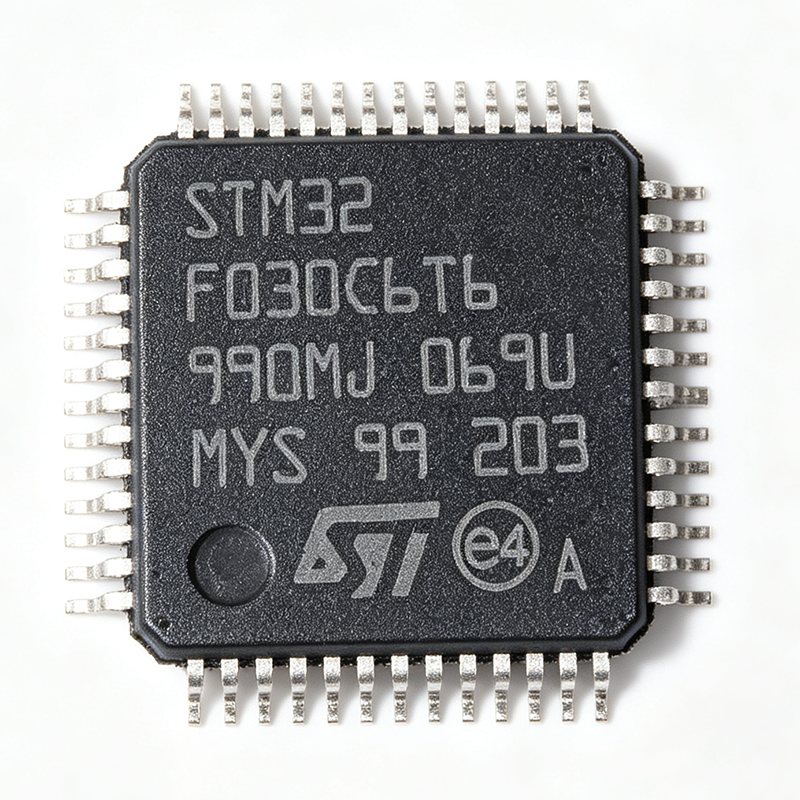
STM32F030C6T6 - 32-bit ARM Cortex-M0 MCU, 32KB Flash | STMicroelectronics
The STMicroelectronics STM32F030C6T6 is a 32-bit ARM Cortex-M0 microcontroller from the STM32F0 series, offering a balanced combination of performance, power efficiency, and peripheral integration. It operates at a core frequency of up to 48 MHz and provides 32 KB of Flash memory and 4 KB of SRAM, making it suitable for a wide range of cost-sensitive embedded applications. The device is housed in a 48-pin LQFP package (7x7 mm) and supports a supply voltage range of 2.4V to 3.6V, with an extended temperature range of -40°C to +85°C. Data verified as of 2026-08-05. What is a microcontroller? A microcontroller (MCU) is a compact integrated circuit designed to govern a specific operation in an embedded system. It integrates a processor core, memory (Flash and SRAM), and programmable input/output peripherals on a single chip. In the system hierarchy, an MCU is a type of embedded processor, which falls under the broader category of integrated circuits (ICs) and semiconductors. The STM32F030C6T6 is a mainstream MCU, positioned between low-end 8-bit devices and high-performance 32-bit processors, offering a cost-effective entry point into the ARM Cortex-M ecosystem. Key features of the STM32F030C6T6 include a 12-bit ADC with up to 10 channels, multiple 16-bit timers, and a full set of communication interfaces including I2C, SPI, and USART. It also features a 32-bit real-time timer, a DMA controller with 5 channels, and a wide range of I/O ports (up to 39 GPIOs). The device supports a variety of low-power modes, including Sleep, Stop, and Standby, enabling energy-efficient designs for battery-powered applications. The ARM Cortex-M0 core provides a simple, energy-efficient architecture with a deterministic interrupt response, making it ideal for real-time control tasks. From a technical perspective, the STM32F030C6T6 is built on a 90nm process technology, balancing cost and performance. The Cortex-M0 core is a von Neumann architecture with a 3-stage pipeline, delivering 0.9 DMIPS/MHz. The device includes a nested vectored interrupt controller (NVIC) with up to 32 interrupt channels, ensuring efficient handling of time-critical events. The Flash memory supports read-while-write, allowing firmware updates without halting the core. The device also includes a unique 96-bit device ID for traceability and security applications. Typical applications include industrial control systems, consumer electronics, home automation, motor control, and sensor interfacing. The rich set of timers and communication interfaces makes it suitable for implementing PWM control, UART-based protocols, and I2C/SPI sensor networks. The low-power modes and wide operating voltage range enable portable and battery-operated devices. When designing with this device, pay attention to the power supply decoupling: place a 100nF capacitor close to each VDD pin and a 4.7uF capacitor on the main supply. Also, configure the boot pins correctly to select the desired boot mode (Flash, System memory, or SRAM). The device supports in-circuit programming via SWD, which simplifies development and production programming. This page synthesizes distributor pricing, drop-in alternatives, and practical design notes not found in the ST datasheet, providing a comprehensive resource for engineers evaluating the STM32F030C6T6.
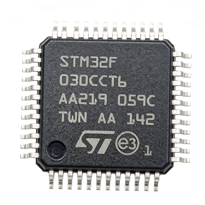
STM32F030CCT6 - 256KB Flash ARM Cortex-M0 MCU | STMicroelectronics
The STM32F030CCT6 is a 32-bit ARM Cortex-M0 microcontroller from STMicroelectronics, featuring 256KB of Flash memory and 32KB of SRAM in a 48-pin LQFP package. It operates at a core frequency of up to 48 MHz and supports a supply voltage range of 2.4V to 3.6V. Data verified as of 2026-08-05. A microcontroller (MCU) is a compact integrated circuit designed to govern a specific operation in an embedded system. It contains a processor core, memory, and programmable input/output peripherals on a single chip. The STM32F030CCT6 belongs to the STM32F0 series, which is part of the broader STM32 family of 32-bit ARM Cortex-M microcontrollers. This hierarchy positions it as a cost-effective, entry-level MCU suitable for a wide range of applications, from industrial control to consumer electronics. Key features include 256KB of Flash memory, 32KB of SRAM, and a rich set of peripherals such as USART, SPI, I2C, ADC, timers, and GPIO. The device supports a wide operating temperature range of -40°C to +85°C and is available in a 48-pin LQFP package, making it suitable for space-constrained designs. The ARM Cortex-M0 core provides a balance of performance and power efficiency, with a 32-bit architecture that simplifies software development. The STM32F030CCT6 is built on a 32-bit ARM Cortex-M0 core with a Harvard architecture, featuring a 3-stage pipeline and a nested vectored interrupt controller (NVIC). It includes a 12-bit ADC with up to 16 channels, multiple 16-bit timers, and a DMA controller for efficient data transfer. The device also supports a variety of low-power modes, including Sleep, Stop, and Standby, enabling energy-efficient operation in battery-powered applications. Typical applications include industrial control systems, motor control, consumer electronics, and IoT devices. The STM32F030CCT6 is well-suited for these applications due to its low cost, low power consumption, and comprehensive peripheral set. For example, in motor control, the advanced timers and ADC enable precise PWM generation and current sensing, while in IoT devices, the low-power modes extend battery life. When designing with this device, ensure proper decoupling of the power supply pins with 100nF capacitors placed close to the VDD pins. Additionally, configure the clock source appropriately, as the internal HSI oscillator provides a 8 MHz clock that can be used for cost-sensitive designs, while an external crystal can be used for higher accuracy. This page synthesizes distributor pricing, drop-in alternatives, and practical design notes not found in the STMicroelectronics datasheet, providing a comprehensive resource for engineers evaluating the STM32F030CCT6.
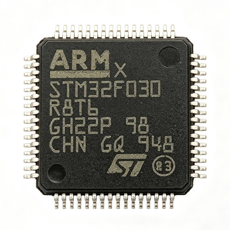
STM32F030R8T6 - 64KB Flash ARM Cortex-M0 MCU | STMicroelectronics
The STMicroelectronics STM32F030R8T6 is a 32-bit ARM Cortex-M0 microcontroller from the STM32F0 series, offering 64KB of Flash memory and 8KB of SRAM in a 64-pin LQFP package. It operates at a core frequency of up to 48 MHz and supports a supply voltage range of 2.4V to 3.6V. Data verified as of 2026-08-05. What is a microcontroller? A microcontroller (MCU) is a compact integrated circuit designed to govern a specific operation in an embedded system. It integrates a processor core, memory (Flash and SRAM), and programmable input/output peripherals on a single chip. The STM32F030R8T6 belongs to the STM32F0 series, which is part of the broader STM32 family of 32-bit ARM Cortex-M microcontrollers. This hierarchy places it within the ARM Cortex-M0 category, a low-power, entry-level core optimized for cost-sensitive applications. Key features include 64KB of Flash memory, 8KB of SRAM, and a rich set of peripherals: five USARTs, two SPI interfaces, two I2C interfaces, one 12-bit ADC with up to 16 channels, and multiple 16-bit timers. The device also includes a 12-bit DAC, a DMA controller, and a real-time clock (RTC). The LQFP-64 package provides 51 GPIO pins, enabling flexible I/O expansion for various applications. The STM32F030R8T6 is built on a 32-bit ARM Cortex-M0 core with a Harvard architecture, achieving 1.25 DMIPS/MHz. It supports a wide operating temperature range of -40°C to +85°C, making it suitable for industrial environments. The device is RoHS compliant and lead-free, aligning with modern environmental standards. Typical applications include industrial control systems, consumer electronics, IoT devices, motor control, and home automation. Its low power consumption and rich peripheral set make it ideal for battery-powered applications and sensor interfacing. When designing with this MCU, ensure proper decoupling of the power supply pins and consider the use of the internal RC oscillator for cost-sensitive designs, or an external crystal for higher accuracy. The device supports in-system programming via SWD, facilitating firmware updates in production. This page synthesizes distributor pricing, drop-in alternatives, and practical design notes not found in the ST datasheet, providing a comprehensive resource for engineers evaluating the STM32F030R8T6.
STM32F030RCT6 - 256KB Flash ARM Cortex-M0 MCU | STMicroelectronics
The STM32F030RCT6 is a 32-bit ARM Cortex-M0 microcontroller from STMicroelectronics, featuring a 48 MHz CPU, 256 KB of Flash memory, and 32 KB of SRAM in an LQFP-64 package. It operates from a 2.4V to 3.6V supply and offers a rich set of peripherals including multiple USARTs, SPIs, I2Cs, ADCs, timers, and GPIOs. Data verified as of 2026-08-05. What is a microcontroller? A microcontroller (MCU) is a compact integrated circuit designed to govern a specific operation in an embedded system. It contains a processor core, memory (Flash and SRAM), and programmable input/output peripherals on a single chip. The STM32F030RCT6 belongs to the STM32F0 series, which is part of the broader STM32 family of 32-bit ARM Cortex-M microcontrollers. This hierarchy places it within the embedded processing domain, where it serves as the central control unit for applications ranging from industrial automation to consumer electronics. Key features include a 48 MHz ARM Cortex-M0 core, 256 KB Flash, 32 KB SRAM, and a comprehensive set of peripherals: 5 USARTs, 2 SPIs, 2 I2Cs, 1 12-bit ADC with up to 16 channels, 8 timers, and up to 51 GPIOs. The device supports a wide operating temperature range of -40°C to +85°C and is available in an LQFP-64 package, making it suitable for space-constrained designs. Technically, the STM32F030RCT6 is built on a 90nm process technology, offering a balance of performance and power efficiency. The ARM Cortex-M0 core is a low-power, high-efficiency processor designed for cost-sensitive applications. The device includes a nested vectored interrupt controller (NVIC), a SysTick timer, and a memory protection unit (MPU) for enhanced reliability. It also features a 12-bit ADC with hardware oversampling, enabling high-resolution analog measurements. Typical applications include industrial control systems, motor control, consumer electronics, IoT devices, and home automation. The rich peripheral set and large Flash memory make it ideal for applications requiring complex firmware and multiple communication interfaces. For example, in an industrial sensor node, the STM32F030RCT6 can interface with sensors via I2C or SPI, process data, and communicate over USART or CAN. When designing with this device, ensure proper decoupling of the power supply pins with 100nF capacitors placed close to each VDD pin. The VDDA pin should be connected to a clean analog supply, and the VREF+ pin should be decoupled with a 1uF capacitor for accurate ADC conversions. The BOOT0 pin must be configured correctly to select the boot mode, and the NRST pin should have an external pull-up resistor and a 100nF capacitor for reliable reset. This page synthesizes distributor pricing, drop-in alternatives, and practical design notes not found in the STMicroelectronics datasheet, providing a comprehensive resource for engineers evaluating the STM32F030RCT6 for their next design.

STM32F031K6U6 - 48MHz Cortex-M0 MCU 32KB Flash | STMicroelectronics
The STM32F031K6U6 is a 32-bit entry-level microcontroller from STMicroelectronics based on the ARM Cortex-M0 core, operating at up to 48 MHz with 32 KB of Flash memory and 4 KB of SRAM in a compact 32-pin UFQFPN (5x5 mm) package with exposed pad. A microcontroller (MCU) is a single-chip embedded processor combining a CPU core, memory, and programmable peripherals. The STM32F031K6U6 belongs to the STM32F0 entry-level family within the STM32 MCU ecosystem, positioned as a migration path from 8-bit and 16-bit MCUs to 32-bit ARM performance. It shares tooling, HAL libraries, and STM32CubeMX configuration software with the wider STM32 portfolio, simplifying future upgrades. Key features include a 12-bit ADC with up to 13 channels, 9 timers, and standard communication interfaces: one I2C, one SPI/I2S, and one USART. The device operates from a 2.0V to 3.6V single supply with integrated POR/PDR reset, and offers a CRC calculation unit and DMA controller for data movement without CPU intervention. Real-time performance is supported by a nested vectored interrupt controller (NVIC) and single-cycle multiplier. The Cortex-M0 architecture executes Thumb instruction sets with deterministic interrupt latency, making the device suitable for real-time control loops. The UFQFPN-32 (QFN family) surface-mount package provides a small 5x5 mm footprint with an exposed thermal pad for grounding, ideal for space-constrained boards. Operating temperature spans -40C to +85C for industrial reliability. Typical applications include industrial control, consumer appliances, IoT sensor nodes, small motor control, and power-management subsystems, where low cost, low power consumption, and adequate peripheral integration matter most. Design tip: decouple VDD pins with 100nF ceramics plus a bulk capacitor, feed VDDA from a clean analog supply to preserve ADC accuracy, and keep NRST properly filtered per the ST datasheet layout guidelines for EMI-robust designs.
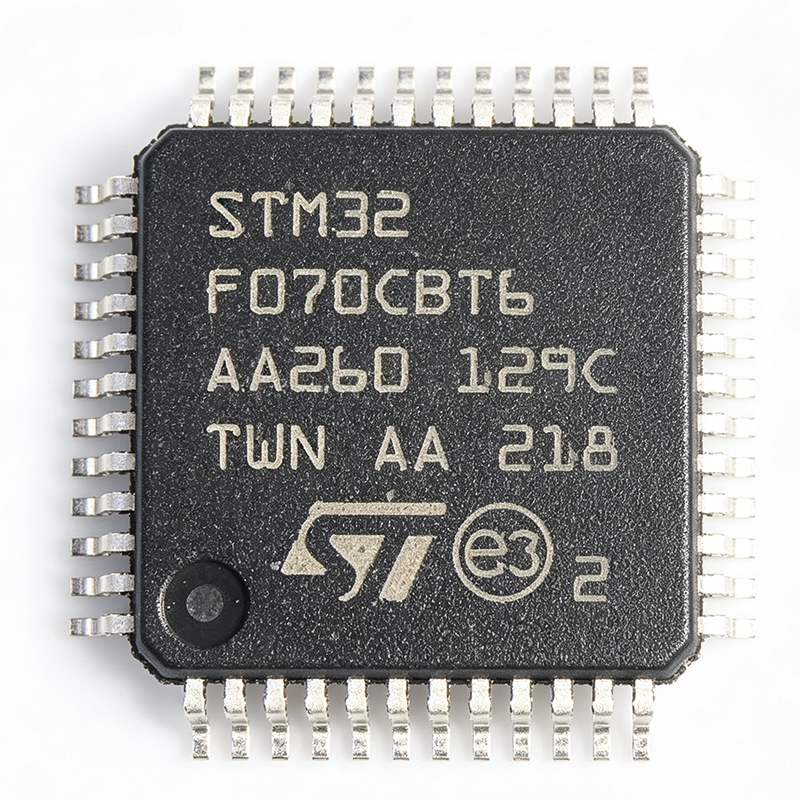
STM32F070CBT6 - ARM Cortex-M0 MCU 128KB Flash | STMicroelectronics
The STMicroelectronics STM32F070CBT6 is a 32-bit ARM Cortex-M0 microcontroller from the STM32F0 series, offering 128KB of Flash memory and 16KB of SRAM in a 48-pin LQFP package. It operates at a core frequency of up to 48 MHz and supports a supply voltage range of 2.4V to 3.6V. Data verified as of 2026-08-05. What is a microcontroller? A microcontroller (MCU) is a compact integrated circuit designed to govern a specific operation in an embedded system. It integrates a processor core, memory (Flash and SRAM), and programmable input/output peripherals on a single chip. The STM32F070CBT6 belongs to the STM32F0 series, which is part of the broader STM32 family of 32-bit ARM Cortex-M microcontrollers. This hierarchy places it within the ARM Cortex-M0 category, a low-power, entry-level core optimized for cost-sensitive applications. Key features include a 12-bit ADC with up to 16 channels, multiple communication interfaces (I2C, SPI, USART), and a variety of timers including advanced-control timers. The device also includes a DMA controller, an RTC, and a CRC calculation unit. The LQFP-48 package provides a compact footprint suitable for space-constrained designs while offering sufficient I/O pins for peripheral connectivity. The STM32F070CBT6 is built on a 32-bit ARM Cortex-M0 core with a Harvard architecture, achieving 1.25 DMIPS/MHz. It includes a nested vectored interrupt controller (NVIC) for efficient interrupt handling and supports both low-power modes (Sleep, Stop, Standby) to optimize energy consumption. The device is designed for a wide range of embedded applications requiring a balance of performance, power efficiency, and cost. Typical applications include industrial control systems, consumer electronics, IoT devices, and home automation. Its rich peripheral set and low-power capabilities make it suitable for sensor interfacing, motor control, and communication protocols. The wide operating temperature range (-40°C to +85°C) ensures reliability in harsh environments. When designing with this MCU, ensure proper decoupling of the power supply pins and consider the use of an external crystal for accurate timing. The device supports in-circuit programming and debugging via SWD, facilitating firmware development and updates. This page synthesizes distributor pricing, drop-in alternatives, and practical design notes not found in the STMicroelectronics datasheet, providing engineers with a comprehensive resource for selection and implementation.
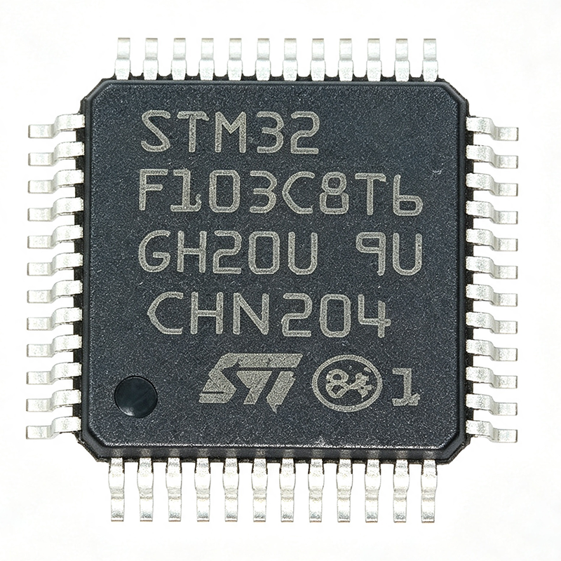
STM32F103C8T6 - 32-bit ARM Cortex-M3 MCU, 64KB Flash | STMicroelectronics
The STM32F103C8T6 is a 32-bit ARM Cortex-M3 microcontroller from STMicroelectronics, featuring 64KB Flash, 20KB SRAM, and operating at up to 72 MHz. It includes multiple communication interfaces (USART, SPI, I2C, USB, CAN) and 12-bit ADCs, making it suitable for industrial control, motor drives, and IoT applications. Available in LQFP-48 package.
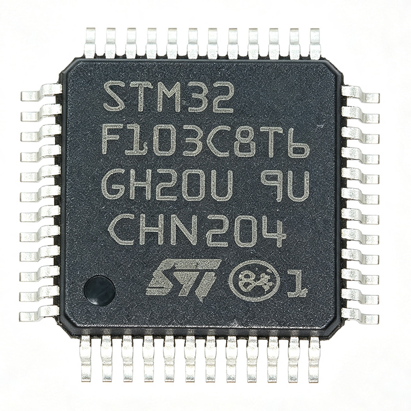
STM32F103C8T6 - 72MHz Cortex-M3 MCU 64KB Flash | STMicroelectronics
The STM32F103C8T6 from STMicroelectronics is a 32-bit ARM Cortex-M3 microcontroller in the medium-density performance line STM32F1 family, operating at up to 72 MHz with 64KB Flash and 20KB SRAM in a 48-pin LQFP package. A microcontroller (MCU) integrates a processor core, memory, and peripherals on a single chip, forming the lowest complete computing tier in the embedded hierarchy: MCU -> embedded processor -> SoC -> application processor. MCUs execute deterministic real-time control tasks in devices ranging from appliances to automotive ECUs. Key features include a 72 MHz Cortex-M3 core with Harvard architecture, 37 GPIOs, two 12-bit ADCs (1 us conversion), three USARTs, two SPI and two I2C interfaces, USB 2.0 full-speed device, CAN 2.0B, and seven 16-bit timers including advanced motor-control PWM timers. Supply range is 2.0V to 3.6V with nested vectored interrupt controller for fast, deterministic interrupt latency. Technically, the Cortex-M3 core implements the Thumb-2 instruction set, combining code density of 8/16-bit MCUs with 32-bit performance. Flash acceleration prefetch buffer sustains 1.25 DMIPS/MHz. The peripheral bus uses APB1 (36 MHz max) and APB2 (72 MHz) bridges off the AHB, and the PLL multiplies the 8 MHz HSE oscillator to 72 MHz. Typical applications include industrial control and PLC I/O modules, motor drives and BLDC inverters using the advanced timers, USB/CAN communication nodes, and IoT sensor nodes. The huge ecosystem (Arduino Blue Pill boards, STM32CubeIDE, open-source toolchains) makes it a default choice for low-cost designs. Design tip: budget the 64KB Flash carefully - bootloader plus USB stacks consume roughly 20KB. For headroom, pin-compatible STM32F103CBT6 doubles Flash to 128KB on the same LQFP-48 footprint.
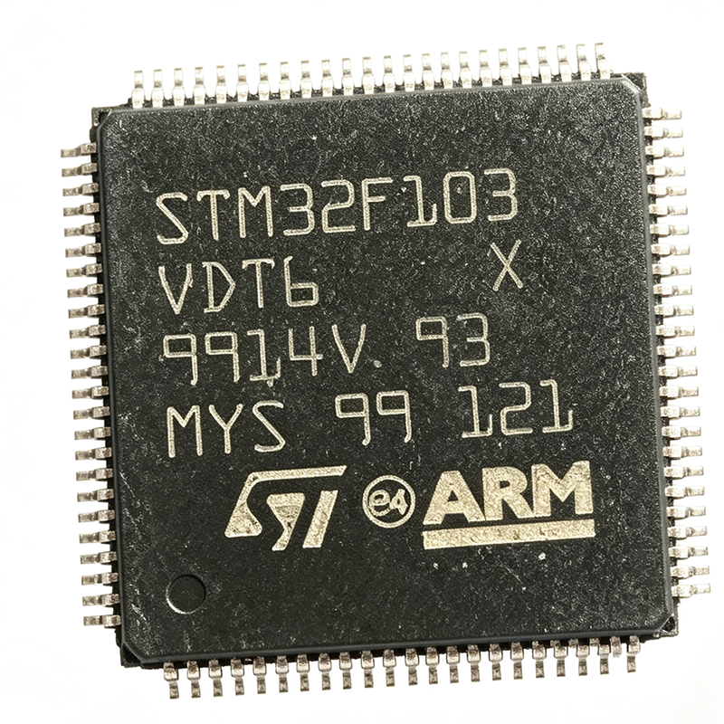
STM32F103VDT6 - 32-bit ARM Cortex-M3 MCU, 384KB Flash | STMicroelectronics
The STM32F103VDT6 is a high-performance 32-bit microcontroller from STMicroelectronics, based on the ARM Cortex-M3 core running at up to 72 MHz. It features 384 KB of Flash memory and 64 KB of SRAM, making it suitable for a wide range of embedded applications. The device is housed in a 100-pin LQFP package (LQFP100) and operates over a temperature range of -40°C to +85°C. An ARM Cortex-M3 microcontroller is a 32-bit RISC processor designed for embedded systems, offering a balance of performance, power efficiency, and rich peripheral integration. It is part of the ARM Cortex-M family, which is widely used in industrial control, consumer electronics, and IoT devices. The Cortex-M3 core includes a hardware multiply and divide unit, Nested Vectored Interrupt Controller (NVIC), and optional Memory Protection Unit (MPU), enabling deterministic and efficient real-time processing. Key features of the STM32F103VDT6 include a 72 MHz CPU with 1.25 DMIPS/MHz, 384 KB Flash, 64 KB SRAM, and a comprehensive set of peripherals: three 12-bit ADCs, four general-purpose 16-bit timers, two advanced-control timers, multiple communication interfaces (USART, SPI, I2C, CAN, USB), and a DMA controller. The device also includes a real-time clock (RTC), a CRC calculation unit, and a serial wire debug (SWD) interface. The STM32F103VDT6 is built on a 0.13 µm embedded Flash process, providing a good balance of performance and power consumption. It supports a wide supply voltage range of 2.0V to 3.6V, with multiple low-power modes (Sleep, Stop, Standby) to optimize energy usage. The rich peripheral set and large memory make it a versatile choice for complex applications. Typical applications include industrial control systems, motor drives, PLCs, medical devices, consumer electronics, and IoT gateways. The device's CAN interface and multiple timers make it particularly well-suited for automotive and industrial networking applications. When designing with this MCU, ensure proper decoupling of the power supply pins and a stable clock source. The internal RC oscillator can be used for basic operation, but an external crystal is recommended for applications requiring precise timing. The SWD interface should be brought out for programming and debugging.