Products (20,000+)

AT91SAM7A1-AU 40MHz ARM7 ROMless MCU | Microchip Technology
AT91SAM7A1-AU

AT91SAM7A1-AU 40MHz ARM7 ROMless MCU | Microchip Technology

The Microchip Technology AT91SAM7A1-AU is a 16/32-bit ARM7-based ROMless microcontroller operating at up to 40 MHz and packaged in a 144-LQFP 20 x 20 mm surface-mount package. It uses a high-performance 32-bit RISC architecture with a dense 16-bit instruction set, embedded ICE debugging support, and a Debug Communication Channel. The device includes 4 KB of internal RAM, while external memory is required for boot code and application storage because the AT91SAM7A1-AU is ROMless. Its broad set of embedded peripherals is intended for industrial, communications, consumer, networking, and automotive-style control systems where a compact microcontroller and mature ARM7 ecosystem simplify product development. The manufacturer datasheet describes the AT91 SAM7 family as using an ARM7TDMI processor with Thumb-based instruction support, combined with high-density on-chip resources and extensive external-memory interfaces. A microcontroller is a dedicated semiconductor that integrates a processor core, memory, peripherals, and interface logic into one device. The ARM7 core provides a 32-bit RISC execution environment, while the Thumb instruction set supports more compact code representations for memory-constrained embedded products. In the AT91SAM7A1-AU, the ROMless architecture gives the designer control over external flash and SRAM implementation, allowing firmware, boot loaders, operating systems, and application data to be managed externally. This is useful when memory size, update strategy, security, or lifecycle requirements exceed what the internal memory can provide. Key characteristics include a maximum operating frequency of 40 MHz, 4 KB of internal RAM, a ROMless design, and a 144-LQFP package measuring 20 x 20 mm. Embedded ICE and the Debug Communication Channel support in-system debugging and communication-oriented development workflows. The large lead count provides access to the device's processor, memory, and peripheral resources, but it also requires careful escape routing and board-layout planning. Because the MCU is not USB-specific, Ethernet-enabled, or application-specific, its suitability depends on matching its external-memory bus, peripheral mix, voltage requirements, and package to the target system. Typical uses include industrial control panels, building automation modules, serial gateways, data acquisition units, motor and actuator controllers, instrument controls, and embedded communications equipment. Designers can use the AT91SAM7A1-AU when they need a general-purpose ARM7 controller with external memory rather than a highly integrated low-power microcontroller. Debug access and a mature ARM7 development ecosystem make it practical for prototypes, legacy platform maintenance, and products requiring predictable peripheral control. A key design consideration is that external memory configuration must be designed around the AT91SAM7A1-AU's bus and memory-controller requirements. Place decoupling and external-memory circuitry close to the associated pins, keep high-speed traces short, and confirm that the power and ground arrangement supports the complete processor, memory, and peripheral load. This page combines device specifications, package information, drop-in alternatives, application guidance, and engineering-oriented design notes to support component selection and board planning.

RFQ Contact
AT91SAM7A2-AU - 30MHz ROMless ARM7 MCU | Microchip | LQFP
AT91SAM7A2-AU

AT91SAM7A2-AU - 30MHz ROMless ARM7 MCU | Microchip | LQFP

The Microchip Technology AT91SAM7A2-AU is a 16/32-bit ARM7-based ROMless microcontroller operating at up to 30 MHz, with 16 KB of internal RAM, 57 general-purpose I/O lines, and a 176-lead LQFP surface-mount package measuring 24 mm by 24 mm. Its ARM7 RISC architecture, mixed 16/32-bit instruction set, and integrated debug support target embedded control systems requiring deterministic real-time behavior without an embedded boot Flash memory. According to the Microchip documentation, the device also supports 64 KB of internal high-speed Flash organized into 512 pages and includes embedded ICE and Debug Communication Channel support. An ARM7-based microcontroller is a 32-bit reduced-instruction-set-computing control device whose Thumb instruction mode supports compact 16-bit code while its 32-bit instruction set handles more complex operations. In the product hierarchy, the AT91SAM7A2-AU is a microcontroller, embedded processor, semiconductor, and programmable control component. It sits above general-purpose computing because its peripherals, interrupt structure, and embedded debug interface are tailored to industrial, communications, and real-time equipment. Principal features include a 30 MHz maximum operating frequency, 16 KB of internal RAM, 57 general-purpose I/O lines, and an integrated 10-bit ADC interface. The device provides PWM channels, USART-based serial communications, and an ARM7TDMI-class RISC core. Its 176-LQFP package exposes substantially more I/O and peripheral connections than small leaded packages, making the device suitable for systems that need broad external connectivity while retaining a conventional leaded package for inspection and assembly. The ROMless architecture is the most important engineering distinction. Because the AT91SAM7A2-AU does not provide a complete application program in its internal Flash, a boot system must load firmware into external memory before normal execution. This arrangement can separate boot code from the main application, permit controlled recovery or firmware updates, and allow the same microcontroller target to support different storage configurations. System designers must therefore budget for external memory, address-bus correctness, startup code, and sufficient flash endurance for the selected update strategy. Typical uses include industrial controllers, serial gateways, data acquisition equipment, building-control interfaces, and embedded access systems. The 57 I/O lines support multiple sensors, actuators, communications ports, and status indicators without requiring a companion I/O expander in moderate-complexity designs. The ADC supports analog measurement, while the USART and PWM resources suit sensor monitoring, actuator control, and supervisory communications. The large LQFP footprint is advantageous for prototype accessibility but requires a 176-lead PCB layout and careful consideration of assembly cost. When designing around this device, verify the external-memory interface, boot configuration, pin multiplexing, and signal levels before committing the PCB. Because the part is ROMless, firmware storage and the boot sequence are part of the system architecture rather than optional software details. A legacy ARM7 design should also include the appropriate debugger, startup routines, clock configuration, and memory timing for the selected external devices. This product overview combines the exact orderable MPN, package and core details, practical firmware considerations, and qualified replacement guidance for engineers evaluating an obsolete ARM7 control platform. It also distinguishes true drop-in interchangeability from newer Cortex-M devices that may provide similar peripherals but require different firmware, package layouts, and board resources.

RFQ Contact
AT91SAM7A3-AU 60MHz ARM7 MCU 256KB Flash 100-LQFP
AT91SAM7A3-AU

AT91SAM7A3-AU 60MHz ARM7 MCU 256KB Flash 100-LQFP

The Microchip Technology AT91SAM7A3-AU is a 32-bit ARM7TDMI microcontroller operating up to 60 MHz, with 256 KB of internal Flash, 32 KB of SRAM, integrated CAN controllers, a 10-bit ADC, timers, and serial communication peripherals in a 100-LQFP package. It belongs to the AT91SAM7A family of ARM Thumb-based embedded-control microcontrollers. An ARM7 microcontroller combines a 32-bit reduced-instruction-set-computing processor with integrated memory and peripherals for embedded control systems. The AT91SAM7A3 architecture combines the ARM7TDMI core with high-speed Flash, SRAM, CAN connectivity, ADC support, timers, and serial interfaces. This hierarchy places the device within the broader category of microcontrollers, embedded processors, and semiconductor components used in industrial, automotive, medical, and communications equipment. The AT91SAM7A3-AU provides 256 KB of high-speed internal Flash and 32 KB of SRAM, allowing firmware and working data to be stored on-chip while reducing external component count. The device operates at up to 60 MHz and includes two 2.0B full CAN controllers, a 10-bit ADC, timers, and multiple serial communication channels. Embedded ICE and Debug Communication Channel support assist development, debugging, and production programming. The AT91SAM7A3 combines a high-performance 32-bit RISC processor with a high-density 16-bit Thumb instruction set. Its integrated CAN capability is useful for networked industrial and automotive control systems, while the ADC supports analog signal acquisition in sensor, measurement, and medical equipment. The 100-LQFP package provides the physical interface required for these mixed signal and communication functions. Typical applications include automotive control modules, industrial automation equipment, medical monitoring systems, CAN-connected embedded controllers, and communications equipment. The integrated CAN controllers are particularly useful when a design requires reliable network communication without adding discrete CAN transceivers, although external transceiver and protection components are still required for physical-layer implementation. Designers should account for the device’s supply voltage limits, peripheral pin multiplexing, clock configuration, and memory map when laying out a PCB. The 100-LQFP footprint should be checked against the manufacturer pin description table before assigning signals. External decoupling, oscillator components, programming access, and CAN transceiver interfaces should follow the reference design guidance in the AT91SAM7A3 documentation. This page combines the verified product characteristics, manufacturer-datasheet information, package details, application guidance, and documented replacement considerations to support faster engineering evaluation and sourcing.

RFQ Contact
AT91SAM7S128D-AU - 55MHz ARM7TDMI MCU, 128KB Flash, USB | Microchip
AT91SAM7S128D-AU

AT91SAM7S128D-AU - 55MHz ARM7TDMI MCU, 128KB Flash, USB | Microchip

The Microchip (formerly Atmel) AT91SAM7S128D-AU is a 32-bit ARM7TDMI RISC microcontroller operating at up to 55 MHz, integrating 128 KB of Flash and 32 KB of SRAM on-chip, and housed in a 64-pin LQFP (10x10 mm) package. It is a member of the SAM7S flash microcontroller family and targets cost-sensitive, high-volume embedded applications that require USB connectivity. A microcontroller (MCU) is a single-chip computer that integrates a CPU core, memory (Flash for program storage, SRAM for runtime data), and a rich set of peripherals (timers, communication interfaces, ADCs, I/O). The AT91SAM7S128D-AU sits within the broader hierarchy: ARM7TDMI core -> ARM7 family -> 32-bit RISC microcontroller -> embedded MCU -> semiconductor IC. Its integrated USB 2.0 Full-Speed Device port differentiates it from competitors by eliminating the need for an external USB transceiver, reducing BOM cost and PCB area in peripheral designs. Key features include a 55 MHz ARM7TDMI core with Thumb instruction set support, 128 KB on-chip Flash, 32 KB SRAM, USB 2.0 Full-Speed Device port, up to 32 peripheral DMA channels, a 10-bit ADC, two USARTs, one UART, two TWI (I2C-compatible) interfaces, an SPI, two 3-channel 16-bit timers, an RTT, a watchdog timer, and a real-time clock. The device operates from 3.0 V to 3.6 V supply and includes an embedded voltage regulator for core logic. Architecturally, the SAM7S series uses a multi-layer AHB/APB bus matrix that allows simultaneous access to peripherals by the CPU and the peripheral DMA controller, eliminating data-transfer bottlenecks typical of single-bus MCUs. The integrated 3.3V LDO regulator and power-on-reset block reduce external component count to a minimum, while the Embedded Flash Controller (EFC) provides Flash read and write access with wear-leveling support. Typical applications include USB peripherals such as HID devices, USB-to-serial adapters, USB barcode scanners, USB keyboards and mice; consumer electronics with embedded control; industrial control nodes; and migration paths for legacy 8-bit designs that require more performance. The aggressive price point and high integration make it well suited to cost-sensitive, high-volume consumer markets. When designing with the AT91SAM7S128D-AU, engineers should ensure the 64-LQFP thermal pad is properly soldered for thermal and electrical performance, and use the integrated voltage regulator's recommended 4.7 µF decoupling capacitors. For USB applications, the D+ and D+ pull-up resistor network must follow the USB 2.0 specification for proper enumeration. This page synthesizes distributor pricing, drop-in same-package alternatives, and practical design notes not found in the manufacturer datasheet alone.

RFQ Contact
AT91SAM7X512B-AU - 512KB Flash ARM7 MCU w/ Ethernet | Microchip
AT91SAM7X512B-AU

AT91SAM7X512B-AU - 512KB Flash ARM7 MCU w/ Ethernet | Microchip

The Microchip AT91SAM7X512B-AU is a 32-bit ARM7TDMI-based flash microcontroller (MCU) running at 55 MHz with 512 KB of embedded Flash and 128 KB of SRAM, housed in a 100-pin LQFP (14x14 mm) package. It integrates a 10/100 Mbps Ethernet MAC, USB 2.0 Full-Speed device port, CAN 2.0A/B controller, and a rich set of serial peripherals including USART, SPI, TWI (I2C), and SSC for audio/I2S streams. The integrated Ethernet MAC embeds a static-MII-less PHY interface and a 16-bit host-side bus that simplifies TCP/IP offload via a hardwired MAC rather than a software stack.

RFQ Contact
AT91SAM7X512B-AUR - 512KB Flash ARM7 MCU 100-LQFP | Microchip
AT91SAM7X512B-AUR

AT91SAM7X512B-AUR - 512KB Flash ARM7 MCU 100-LQFP | Microchip

The Microchip AT91SAM7X512B-AUR is a 32-bit ARM7TDMI-based flash microcontroller integrating 512KB of program flash and 128KB of SRAM on-chip, operating at up to 55 MHz from a 1.65V–1.95V core / 3.0V–3.6V I/O supply, housed in a 100-pin LQFP (14x14 mm) package supplied on tape and reel. What is an ARM7-based flash microcontroller? An ARM7TDMI MCU is a 32-bit RISC processor with Thumb 16-bit compressed instruction support, integrating flash program memory, SRAM, peripherals, and often connectivity blocks such as Ethernet MAC and CAN on a single die. In the broader taxonomy it sits below ARM Cortex-M parts but above 8/16-bit 8051/AVR devices, occupying the industrial/embedded connectivity tier where deterministic 32-bit performance and integrated wired networking matter more than ultra-low power. Key features of the AT91SAM7X512B-AUR include an integrated 10/100 Ethernet MAC with MII/RMII interface, a CAN 2.0B controller, a USB 2.0 Full-Speed Device port, an 8-channel 10-bit ADC, four 16-bit timers, an 8-bit RTC, and a peripheral DMA controller that offloads data movement from the core. The embedded flash controller supports in-system programming and bootloader operation from USB or UART. Architecturally, the SAM7X512B uses a three-layer AHB bus matrix connecting the core, flash controller, peripheral DMA, and a bridge to APB peripherals, allowing parallel bus transactions that improve sustained throughput for Ethernet and USB traffic. The ARM7TDMI core's three-stage pipeline delivers roughly 0.9 MIPS/MHz, giving ~49 Dhrystone MIPS at 55 MHz. Typical applications include industrial gateways, building-automation controllers, point-of-sale terminals, CAN-based sensor nodes, and embedded Ethernet bridges. Integrated Ethernet plus CAN makes the part especially suitable for protocol-conversion bridges between factory-floor CAN networks and IP backhaul. When designing with the AT91SAM7X512B-AUR, verify the dual-rail supply (1.8V VDDCORE plus 3.3V VDDIO) and provide bulk decoupling near each power pin. Microchip designates the SAM7X family as not recommended for new designs (NRND); the AT91SAM7XC512B is the pin-compatible successor with optional AES/TDES crypto accelerators. This page synthesizes distributor pricing, drop-in alternatives, and practical design notes not found in the standalone manufacturer datasheet, including a v3.9-aligned alternatives list of same-brand and cross-brand drop-in options verified for package and pin compatibility.

RFQ Contact
AT91SAM9260B-CU - ARM926EJ-S MCU 180MHz 217-LFBGA | Microchip
AT91SAM9260B-CU

AT91SAM9260B-CU - ARM926EJ-S MCU 180MHz 217-LFBGA | Microchip

The Microchip Technology (formerly Atmel) AT91SAM9260B-CU is a SMART 32-bit ARM926EJ-S embedded microprocessor running at up to 180 MHz, packaged in a 217-ball LFBGA (15x15 mm). It integrates 32 KB of ROM, 8 KB of SRAM, and a 6-layer bus architecture that delivers up to six simultaneous 32-bit internal buses for parallel data movement. Key features include Full-Speed USB Host and Device ports, a 10/100 Ethernet MAC with RMII/MII interface, an image sensor interface (ISI), a MultiMedia Card Interface (MCI), I2S audio, three USARTs, two UARTs, SPI, TWI (I2C), Timer Counters, a Synchronous Serial Controller (SSC), and an ADC. The 6-layer matrix bus architecture provides high internal bandwidth, which makes the part suitable for multimedia, image-capture, and connected-embedded applications. The 'B' silicon revision improves upon the original AT91SAM9260 with errata fixes and refined peripheral behavior. The AT91SAM9260 family occupies the ARM9-based MPU segment of the Microchip SAM9 portfolio. As an ARM926EJ-S device with a memory management unit (MMU), it runs full operating systems such as Linux, WinCE, and MQX. Compared to Cortex-M microcontrollers, it offers higher compute throughput, richer connectivity peripherals, and OS support at the cost of higher power and a more complex toolchain. Typical applications include human-machine interfaces (HMIs), industrial control panels, image-capture and machine-vision front-ends, networked point-of-sale terminals, building automation gateways, and low-cost Ethernet/USB-connected embedded nodes where an MMU-capable SoC is required. When designing with this device, ensure the LFBGA-217 layout uses the manufacturer-recommended 8-layer PCB stack-up, a 12 MHz or similar main oscillator, and a regulated 1.8V core / 3.3V I/O supply pair to satisfy the SAM9260 power-domain requirements. This page synthesizes distributor pricing, drop-in alternatives, and practical design notes not found in the manufacturer datasheet, giving engineers a single decision-grade source.

RFQ Contact
AT91SAM9G20B-CU - 400MHz ARM926 MPU, 217-LFBGA | Microchip
AT91SAM9G20B-CU

AT91SAM9G20B-CU - 400MHz ARM926 MPU, 217-LFBGA | Microchip

The Microchip AT91SAM9G20B-CU is a 400 MHz ARM926EJ-S embedded microprocessor (MPU) housed in a 217-ball LFBGA (15x15 mm) package, integrating fast ROM/RAM, a 10/100 Ethernet MAC, USB host/device interfaces with on-chip transceivers, and an image sensor interface. It belongs to the SAM9G family of smart ARM-based MPUs designed for connected embedded systems. The 'B' suffix designates the revision with the higher 400 MHz core clock versus the legacy 200/266 MHz SAM9G, while the 'CU' suffix denotes the 217-LFBGA industrial-grade package variant. An ARM926EJ-S microprocessor is a 32-bit RISC CPU core featuring the ARMv5TEJ instruction set with Jazelle Java acceleration, MMU, and DSP extensions, designed for embedded applications requiring full operating-system support such as Linux and Windows Embedded Compact. In the broader system hierarchy, the AT91SAM9G20 sits below application processors and above microcontrollers (MCUs), bridging the gap between deterministic MCU-class peripherals and rich-OS-capable CPUs. The 217-LFBGA package is part of the fine-pitch BGA surface-mount family requiring reflow soldering and X-ray or AOI inspection. Key features include an ARM926EJ-S core with 32 KB instruction cache and 32 KB data cache, 64 KB internal SRAM, 16 KB ROM containing the bootloader, and an external bus interface supporting DDR/LPDDR, NAND Flash, and SDRAM. Communication peripherals cover two USB 2.0 Full-Speed ports (host and device), a 10/100 Ethernet MAC with MII/RMII, an Image Sensor Interface (ISI), two SSC/SPI, four UART, two TWI (I2C), and a high-speed multimedia card interface (HSMCI). Operating voltage is 0.9-1.1 V core with 1.65-3.6 V I/O and memory. Typical applications include industrial HMI panels, point-of-sale terminals, barcode scanners, building automation gateways, portable medical data terminals, and Linux-based IoT edge nodes. The combination of Ethernet, dual USB, image sensor input, and DDR controller enables a true single-chip system design without an external bus-master companion. Compared to microcontrollers in the same generation, the AT91SAM9G20 provides full MMU support and Linux BSP availability from Microchip, simplifying migration from MCU-class designs when memory protection and complex OS features are required.

RFQ Contact
AT97SC3204-U2A1A-10 - TPM 1.2 Crypto Controller | Microchip | 28-TSSOP
AT97SC3204-U2A1A-10

AT97SC3204-U2A1A-10 - TPM 1.2 Crypto Controller | Microchip | 28-TSSOP

The Microchip AT97SC3204-U2A1A-10 is an AVR-based CryptoController Trusted Platform Module (TPM) compliant with TCG (Trusted Computing Group) TPM 1.2 specifications, housed in a 28-pin TSSOP package (4.40 mm body width). It is a fully integrated hardware security module designed for embedded systems that need to perform RSA/SHA-1 cryptographic operations, secure key storage, platform attestation, and TWI (I²C-compliant) host communication. The device is part of Microchip's AT97SC3204 family and is rated for the industrial temperature range. A Trusted Platform Module (TPM) is a dedicated hardware security controller (a type of microcontroller + EEPROM security IC) that provides a tamper-resistant root of trust for computing platforms. In the broader taxonomy it sits under security IC -> authentication IC -> application-specific microcontroller, and ultimately under semiconductor. TPMs perform RSA encryption/decryption, SHA-1 hashing, random number generation, and sealed key binding/unbinding, all while keeping private keys inside a hardware boundary that resists software-level extraction. Key features include a hardware RNG (FIPS 140-2 compliant random number generator), an integrated Atmel AVR core for command processing, on-chip non-volatile EEPROM key storage, and a TWI/I²C host interface. The device operates from a 3.3 V supply, supports I²C at standard and fast-mode rates, and provides Endorsement Key (EK) pre-provisioning under the suffix -10 (signed EK). The 28-TSSOP footprint and standard TPM pinout allow drop-in replacement on compliant mainboard headers. The architecture combines an 8-bit AVR MCU, a crypto-acceleration block for RSA-1024/2048 and SHA-1, secure EEPROM for persistent keys, and a TWI slave controller. This partitioning keeps the host CPU free of cryptographic computation and keeps private keys bound to hardware for the platform's lifetime. Typical applications include commercial desktop and notebook PCs, server motherboards, embedded industrial controllers requiring secure boot, network equipment needing platform attestation, and any TCG-compliant system that requires hardware-bound credential storage. The TWI interface integrates with standard I²C controllers on most SBCs and SoCs. Designers should ensure the LPC (Low Pin Count) interface is correctly wired to the host chipset's TPM header and that the firmware stack (BIOS/UEFI TCG driver) is enabled in BIOS. The EK variant (-10) is signed and ready for attestation flows; the EK-less variant is suitable for non-attestation use cases. This page combines distributor pricing snapshots, drop-in alternative analysis, and design notes not included in the manufacturer datasheet addendum, providing engineering perspective beyond raw specifications.

RFQ Contact
ATMEGA103-6AC - 8-Bit AVR MCU, 6MHz, 128KB Flash | Microchip
ATMEGA103-6AC

ATMEGA103-6AC - 8-Bit AVR MCU, 6MHz, 128KB Flash | Microchip

The Microchip Technology ATMEGA103-6AC is an 8-bit AVR enhanced RISC microcontroller with 128KB of In-System Programmable Flash (64K x 16), operating at up to 6 MHz from a 5V supply, housed in a 64-pin TQFP (14 x 14 mm) package. A microcontroller is a single-chip computer that integrates a processor core, program memory, data memory, and peripherals such as timers, UART, and analog-to-digital converters onto one die. In the embedded systems hierarchy, the AVR ATmega family sits within the broader class of 8-bit microcontrollers, competing with architectures such as Microchip PIC, 8051, and Freescale HC08. The AVR architecture uses a Harvard structure with most instructions executing in a single clock cycle, giving high code efficiency and MIPS-per-MHz. Key features of the ATMEGA103-6AC include 121 powerful instructions (most single-cycle), 128KB of In-System Reprogrammable Flash, 4KB of internal SRAM, and 4KB of EEPROM for non-volatile data storage. The 6 MHz speed grade with a 5V supply targets cost-sensitive commercial-temperature applications where maximum performance is not required. The large 128KB Flash makes it suitable for firmware-heavy applications such as protocol stacks and menu-driven HMI code. Technically, the ATmega103 uses an AVR enhanced RISC core with 32 general-purpose working registers directly connected to the ALU, allowing two independent registers to be accessed in one instruction executed in one clock cycle. This delivers throughput approaching 1 MIPS per MHz. Peripherals typically include an 8-channel 10-bit ADC, multiple timer/counters with PWM, UART for serial communication, and SPI for synchronous serial interfacing. Typical applications include industrial control panels, building automation nodes, battery-backed instrumentation, and legacy embedded products whose firmware was designed around the ATmega103 memory map and pinout. Design consideration: the 5V-only supply and 6 MHz limit mean new designs should normally select the pin-compatible ATmega128 family, which runs to 16 MHz with richer peripherals while sharing the 64-TQFP footprint. This page synthesizes distributor pricing, verified drop-in alternatives such as the ATmega128 series, and practical sourcing notes not found in the manufacturer datasheet.

RFQ Contact
ATMEGA103-6AI - 8-Bit AVR MCU, 6MHz, 128KB Flash | Microchip
ATMEGA103-6AI

ATMEGA103-6AI - 8-Bit AVR MCU, 6MHz, 128KB Flash | Microchip

The Microchip Technology ATMEGA103-6AI (originally Atmel) is an 8-bit AVR enhanced RISC microcontroller delivering 6 MHz maximum clock speed, 128 KB of in-system programmable Flash (64K x 16 organization), and 4 KB SRAM plus 4 KB EEPROM, housed in a 64-pin TQFP (14x14 mm) package operating from a 5V supply. An AVR microcontroller is a class of 8-bit Harvard-architecture MCUs in which program memory and data memory occupy separate address spaces, allowing most instructions to execute in a single clock cycle. Within the power-management hierarchy, the ATmega103 sits in the high-memory general-purpose microcontroller tier, sitting above the ATmega603 (64 KB Flash) sibling and pre-dating the pin-compatible ATmega128. Key features include the AVR enhanced RISC core with 121 powerful instructions (most single-cycle), 128 KB in-system reprogrammable Flash, 4 KB internal SRAM, 4 KB EEPROM, an 8-channel 10-bit ADC, UART, SPI, and a wide -40C to +85C industrial operating temperature range denoted by the 'I' suffix in the part number. The 6 MHz speed grade ('6') covers 5V operation. Architecturally, the ATmega103 uses a low-power CMOS process with a fast-access RISC register file of 32 general-purpose 8-bit registers directly connected to the ALU, enabling single-cycle execution that yields throughput of roughly 6 MIPS at 6 MHz. Nonvolatile memory is organized for in-system reprogramming via SPI, and the memory map includes external memory expansion capability. Typical applications include legacy industrial control systems, building automation controllers, instrumentation, and embedded products designed in the late 1990s and early 2000s that still require AVR compatibility at the 128 KB memory point. Design consideration: because this is a 5V-only part with a 6 MHz ceiling, new designs should evaluate the pin-compatible, higher-performance ATmega128 family instead; ATmega103-mode compatibility is retained in the ATmega128 via an M103C fuse. This page consolidates distributor pricing, drop-in alternative cross-references, and practical migration design notes not found together on the manufacturer datasheet.

RFQ Contact
ATMEGA103L-4AC - 8-Bit AVR MCU 4MHz 128KB TQFP-64 | Microchip
ATMEGA103L-4AC

ATMEGA103L-4AC - 8-Bit AVR MCU 4MHz 128KB TQFP-64 | Microchip

The Microchip Technology (Atmel) ATMEGA103L-4AC is a low-power CMOS 8-bit microcontroller based on the AVR enhanced RISC architecture, delivering up to 4 MHz operation at 2.7 V to 5.5 V with 128 KB of in-system programmable Flash, 4 KB of SRAM, and 64 KB of optional external memory addressing, housed in a 64-pin TQFP (14x14 mm) package. An 8-bit AVR microcontroller is a single-chip processor that executes most instructions in a single clock cycle using a Harvard-architecture RISC core with 32 general-purpose working registers. Within the system hierarchy, the MCU sits at the heart of an embedded system: flash memory stores program code, SRAM holds runtime variables, and integrated peripherals (UARTs, SPI, timers) interface with sensors and actuators, making a discrete CPU-plus-peripherals chipset unnecessary. Key features of the ATMEGA103L-4AC include 128 KB (64K x 16) of In-System Programmable (ISP) Flash, dual USARTs for serial communication, an SPI serial interface, two 8-bit and two 16-bit timers/counters with PWM outputs, and an 8-channel external interrupt capability. The AVR core's single-cycle instruction execution yields up to 4 MIPS at the 4 MHz maximum clock rating of this L-suffix (2.7 V to 5.5 V) commercial-grade device. Architecturally, the ATmega103 separates instruction and data buses, allowing fast register-to-register operations and efficient C-code compilation. External memory expansion (up to 64 KB) is supported through the multiplexed address/data bus on Ports A and C with WR/RD strobes on Port G, enabling designs requiring large data buffers. Typical applications include legacy industrial control panels, battery-powered instruments, building automation nodes, and embedded systems where the 4 MHz low-voltage rating supports long-battery-life or noise-limited 3.3 V designs. Design consideration: this part is end-of-life per distributor status data, so new designs should target the ATmega128 family, and existing boards should secure remaining stock or qualify a drop-in variant before replenishment runs out. This page adds value beyond the manufacturer datasheet by consolidating drop-in alternatives, lifecycle status, pricing context, and practical design notes in one engineer-facing reference.

RFQ Contact
ATMEGA103L-4AI - 8-Bit AVR MCU 128KB 4MHz TQFP-64 | Microchip
ATMEGA103L-4AI

ATMEGA103L-4AI - 8-Bit AVR MCU 128KB 4MHz TQFP-64 | Microchip

The Microchip Technology ATMEGA103L-4AI is an 8-bit AVR enhanced RISC microcontroller executing up to 4 MHz with 128KB (64K x 16) of in-system programmable FLASH and 4KB of SRAM, housed in a 64-pin TQFP (14x14 mm) package for industrial temperature ranges. An 8-bit AVR microcontroller is a single-chip processor built on the AVR enhanced RISC architecture, in which most of its powerful instructions execute in a single clock cycle. In the embedded-systems hierarchy it sits as the central processing element of a board, above discrete logic and below 32-bit application processors, and belongs to the broader family of microcontroller units (MCUs) that integrate program memory, data memory, timers, and communication peripherals on one die. Key features of the ATMEGA103L-4AI include 121 powerful instructions with mostly single-clock-cycle execution, 128K bytes of in-system reprogrammable FLASH program memory, and serial programming interfaces. The L suffix denotes the low-voltage variant, while the AI suffix denotes the industrial temperature grade supplied in the 64-lead thin quad flat package (TQFP-64). Architecturally, the device uses a Harvard-structure AVR core with separate program and data buses, allowing one instruction to be fetched while another is decoded and executed, which sustains throughput approaching 1 MIPS per MHz of clock. On-chip peripherals include an 8-channel 10-bit ADC, two 8-bit and two 16-bit timers with PWM, an SPI serial port, and a UART, providing complete system control in a single chip. Typical applications include legacy industrial control boards, instrument front panels, building automation nodes, and communication equipment controllers. The low-voltage operation suits 3.3V systems, while the industrial temperature range supports factory-floor environments where consumer-grade parts cannot survive. A key design consideration is that this part is mature/obsolete for new designs; engineers starting new boards should evaluate the pin-compatible ATmega128 family, which offers an ATmega103 compatibility mode and higher clock speeds. Verify FLASH endurance and programming-tool support before committing to new production. This page synthesizes distributor availability data, drop-in alternative analysis, and practical design notes not found in the manufacturer datasheet, with pricing referenced as of 2026-09-15.

RFQ Contact
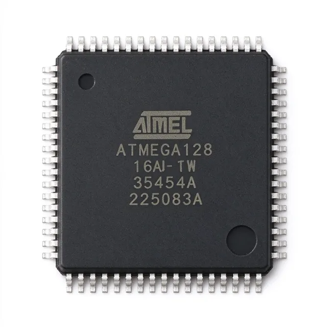
ATMEGA128-16AC - 8-bit AVR MCU 16MHz 128KB Flash | Microchip
ATMEGA128-16AC

ATMEGA128-16AC - 8-bit AVR MCU 16MHz 128KB Flash | Microchip

The Microchip Technology ATMEGA128-16AC is a low-power 8-bit AVR microcontroller with 128KB in-system programmable Flash, 16MHz maximum clock frequency, and 4KB SRAM, housed in a 64-pin TQFP (14x14 mm) package. An 8-bit microcontroller is an integrated circuit that contains a processor core, memory, and programmable input/output peripherals on a single chip, executing control and data-processing tasks in embedded systems. Within the product hierarchy, the ATmega128 sits in the AVR ATmega family of enhanced RISC MCUs, which belongs to the broader class of general-purpose microcontrollers within semiconductor-based embedded processing. The AVR architecture executes most instructions in a single clock cycle, achieving throughput approaching 1 MIPS per MHz. Key features of the ATMEGA128-16AC include 133 powerful AVR instructions with mostly single-cycle execution, 32 general-purpose working registers, 128KB of ISP Flash with 10,000 write-cycle endurance, 4KB EEPROM rated for 100,000 write cycles, and a rich peripheral set: two 8-bit and two 16-bit timers with PWM, two USARTs, SPI, TWI (I2C-compatible), an 8-channel 10-bit ADC, analog comparator, watchdog timer, and JTAG boundary-scan/on-chip-debug support. Architecturally, the AVR uses a Harvard structure with separate program and data buses, allowing simultaneous Flash instruction fetch and data access. In-system programmability permits firmware updates after board assembly, and the boot Flash section supports self-programming for field upgrades. Typical applications include industrial control and automation nodes, embedded instrumentation and test equipment, motor-control and power-supervision systems, and legacy embedded designs requiring extended 128KB program memory with 5V-tolerant I/O. When designing with this part, remember the -16AC is the commercial temperature grade (0C to +70C); select the -16AI industrial grade for -40C to +85C environments, and budget for a 4.5V to 5.5V supply since 16MHz operation is not supported at 3.3V. This page synthesizes distributor pricing, drop-in alternatives, complete 64-pin pinout data, and practical design notes not found in the manufacturer datasheet alone.

RFQ Contact
ATMEGA128-16AI - 8-bit AVR MCU 16MHz 128KB Flash | Microchip
ATMEGA128-16AI

ATMEGA128-16AI - 8-bit AVR MCU 16MHz 128KB Flash | Microchip

The Microchip (Atmel) ATMEGA128-16AI is an 8-bit AVR RISC microcontroller with 128KB in-system programmable flash, 4KB SRAM, and 4KB EEPROM, executing up to 16 MIPS at 16MHz in a 64-pin TQFP (14x14 mm) package rated for the industrial temperature range. An 8-bit AVR microcontroller is a Harvard-architecture processor that fetches instructions and data over separate buses, allowing most of its 133 powerful instructions to execute in a single clock cycle. Within the product hierarchy, the ATmega128 sits in the ATmega family of flash-based microcontrollers - below the ATmega1280/1281 mega-AVR devices and above the ATmega64 - and functions as a complete embedded system-on-chip integrating CPU, memory, timers, communication peripherals, and an ADC. Key features include 128KB of self-programmable flash with a boot loader section, dual USARTs, SPI, TWI (I2C), an 8-channel 10-bit ADC, two 8-bit and two 16-bit timers with PWM, and an on-chip JTAG interface for boundary-scan and on-chip debugging. The device operates from 4.5V to 5.5V at 16MHz (per the -16 speed grade), delivering deterministic single-cycle execution without pipelining penalties. Architecturally, the ATmega128 combines 32 general-purpose working registers directly connected to the ALU, enabling true single-cycle arithmetic in one clock. XMEM interface support expands external memory addressing up to 64KB, useful for data-logging and legacy 8051-style designs migrating to AVR. Power management includes six sleep modes, allowing current consumption optimization from active operation down to microamp levels in power-down. Typical applications include industrial control and factory automation nodes, legacy ATmega103 PCB upgrades (the ATmega128 is 100% pin compatible with the ATmega103), embedded instrumentation, motor control panels, and building automation controllers where a mature, well-documented 5V MCU simplifies design. Design consideration: the -16 grade requires 4.5V to 5.5V operation; for 3.3V systems use the 8MHz ATmega128L variant instead, and budget JTAG pin sharing (PF4-PF7) when planning ADC channel allocation. This page synthesizes distributor pricing context, drop-in alternatives, pin-level design notes, and comparison data not found in a single manufacturer datasheet.

RFQ Contact
ATMEGA128-16AJ - 16MHz 128KB 8-Bit AVR MCU | Microchip
ATMEGA128-16AJ

ATMEGA128-16AJ - 16MHz 128KB 8-Bit AVR MCU | Microchip

The Microchip Technology ATMEGA128-16AJ is an 8-bit AVR RISC microcontroller operating at 16 MHz, with 128 KB of programmable flash memory, 4 KB SRAM, and 4 KB EEPROM in a 64-pin TQFP package. It combines an 8-channel 10-bit ADC, JTAG debugging, and serial peripherals for embedded control systems. A microcontroller is a programmable integrated circuit that executes firmware, reads inputs, controls outputs, and manages embedded-system functions. This ATmega device belongs to the AVR family of 8-bit RISC microcontrollers, combining flash-backed program storage, SRAM, EEPROM, timers, serial communications, and analog conversion. Its architecture is designed for compact control, measurement, communication, and automation products. Verified product information identifies a 16 MHz AVR core, 128 KB flash memory, 4 KB SRAM, and 4 KB EEPROM. The ATMEGA128-16AJ also provides an 8-channel 10-bit ADC and JTAG interface. Its 64-TQFP package exposes the device's I/O and communication resources while supporting surface-mount PCB assembly. The AVR core provides an 8-bit processing platform with an instruction set designed for efficient embedded control. Program storage is 128 KB, while the 4 KB SRAM supports working variables and application state. The 4 KB EEPROM provides nonvolatile storage for parameters, calibration data, configuration values, and other information that must survive power removal. Typical applications include industrial controllers, building automation equipment, data-acquisition modules, motor and relay-control systems, communication equipment, and embedded instruments. The 10-bit ADC is suitable for analog sensor interfaces, while the JTAG interface supports hardware-assisted programming and debugging workflows. The exact peripheral availability and electrical limits should be confirmed against the manufacturer datasheet before design release. Designers should preserve the required power, decoupling, clock, programming, and JTAG connections, and should account for the 64-pin TQFP footprint and exposed ground requirements. The exact operating-voltage range, pin names, electrical timing values, and package-specific details are not present in the supplied verified data and are marked as needed below rather than inferred.

RFQ Contact
ATMEGA128-16AN - 8-Bit AVR MCU 128KB 16MHz TQFP-64 | Microchip
ATMEGA128-16AN

ATMEGA128-16AN - 8-Bit AVR MCU 128KB 16MHz TQFP-64 | Microchip

The Microchip Technology ATMEGA128-16AN is an 8-bit AVR RISC microcontroller delivering up to 16 MIPS throughput at 16 MHz, with 128 KB of In-System Programmable FLASH, 4 KB SRAM, and 4 KB EEPROM, housed in a 64-pin TQFP (14x14 mm) package. It operates from 4.5V to 5.5V and supports on-chip JTAG debugging. An 8-bit AVR microcontroller is a single-chip processor built on the AVR enhanced RISC architecture, in which most of the 131 instructions execute in a single clock cycle. Within the system hierarchy, the microcontroller sits between simple logic ICs and application processors, integrating CPU, program memory, data memory, timers, and communication peripherals into one device for embedded control tasks. Key features include 53 general-purpose I/O lines, 32 general-purpose working registers, four flexible timers/counters with compare modes and PWM, and an 8-channel 10-bit A/D converter. Dual USARTs, a byte-oriented Two-Wire Interface (I2C-compatible), and a hardware SPI port provide multi-protocol connectivity for sensors, displays, and industrial networks. Technically, the fully static core sustains performance from DC to 16 MHz, while the Read-While-Write FLASH allows code updates during operation. An RTC with separate oscillator, JTAG boundary-scan, and an ATmega103 compatibility mode (via the M103C fuse) simplify legacy design migration. This version is rated at 16 MHz at 4.5-5.5V with a -40C to +85C industrial temperature rating. Typical applications include industrial automation control panels, HVAC and building-management systems, battery-monitoring instrumentation, and motor-control nodes using the PWM channels. Design consideration: for lowest power consumption in idle and power-down modes, configure unused I/O pins as inputs with internal pull-ups and use the power-reduction registers to clock-gate unused peripherals. This page synthesizes distributor pricing, drop-in alternatives, and practical design notes not found in the manufacturer datasheet.

RFQ Contact
ATMEGA128-16ANR - 8-Bit AVR MCU 128KB 16MHz TQFP-64 | Microchip (Tape & Reel)
ATMEGA128-16ANR

ATMEGA128-16ANR - 8-Bit AVR MCU 128KB 16MHz TQFP-64 | Microchip (Tape & Reel)

The Microchip Technology ATMEGA128-16ANR is an 8-bit AVR RISC microcontroller delivering up to 16 MIPS throughput at 16 MHz, with 128 KB of In-System Programmable FLASH, 4 KB SRAM, and 4 KB EEPROM, housed in a 64-pin TQFP (14x14 mm) package. It operates from 4.5V to 5.5V and supports on-chip JTAG debugging. An 8-bit AVR microcontroller is a single-chip processor built on the AVR enhanced RISC architecture, in which most of the 131 instructions execute in a single clock cycle. Within the system hierarchy, the microcontroller sits between simple logic ICs and application processors, integrating CPU, program memory, data memory, timers, and communication peripherals into one device for embedded control tasks. Key features include 53 general-purpose I/O lines, 32 general-purpose working registers, four flexible timers/counters with compare modes and PWM, and an 8-channel 10-bit A/D converter. Dual USARTs, a byte-oriented Two-Wire Interface (I2C-compatible), and a hardware SPI port provide multi-protocol connectivity for sensors, displays, and industrial networks. Technically, the fully static core sustains performance from DC to 16 MHz, while the Read-While-Write FLASH allows code updates during operation. An RTC with separate oscillator, JTAG boundary-scan, and an ATmega103 compatibility mode (via the M103C fuse) simplify legacy design migration. This version is rated at 16 MHz at 4.5-5.5V with a -40C to +85C industrial temperature rating. Typical applications include industrial automation control panels, HVAC and building-management systems, battery-monitoring instrumentation, and motor-control nodes using the PWM channels. Design consideration: for lowest power consumption in idle and power-down modes, configure unused I/O pins as inputs with internal pull-ups and use the power-reduction registers to clock-gate unused peripherals. This page synthesizes distributor pricing, drop-in alternatives, and practical design notes not found in the manufacturer datasheet.

RFQ Contact
ATMEGA128-16AU - 8-Bit AVR MCU, 128KB Flash, 16MHz | Microchip
ATMEGA128-16AU

ATMEGA128-16AU - 8-Bit AVR MCU, 128KB Flash, 16MHz | Microchip

The Microchip Technology ATMEGA128-16AU is a high-performance, low-power 8-bit AVR RISC microcontroller with 128KB of In-System Programmable Flash, 4KB SRAM, 4KB EEPROM, an 8-channel 10-bit ADC, and a JTAG interface for on-chip debugging, delivered in a 64-pin TQFP (14x14 mm) package operating at up to 16 MHz. An 8-bit AVR microcontroller is a single-chip processor built on the AVR enhanced RISC architecture, in which most instructions execute in a single clock cycle. Within the power-management and embedded-control hierarchy, it functions as the central computing element of a system, replacing discrete logic and analog control circuitry while offering flash-based field reprogrammability. Key features include 128KB self-programmable Flash with a boot section for in-application programming, 4KB internal SRAM, 4KB EEPROM for non-volatile parameter storage, and throughput approaching 16 MIPS at 16 MHz, allowing designers to optimize power consumption versus processing speed. Technically, the ATmega128 combines an 8-channel 10-bit A/D converter with an external-memory interface (up to 64KB external data space via PORTA/PORTC multiplexed addressing), two 8-bit and two 16-bit timers with PWM outputs, two USARTs, SPI, and a Two-Wire Interface, plus a JTAG boundary-scan and debug port. The AVR Harvard architecture with 32 general-purpose registers enables efficient C-compiled code execution. Typical applications include industrial control and automation nodes, general embedded systems, data loggers, and legacy ATmega103 upgrades, since the ATmega128 is 100% pin compatible with ATmega103 and can replace it on existing PCBs. A key design consideration is supply voltage: the 16 MHz -16AU speed grade requires 4.5V to 5.5V operation; the ATmega128L variant is needed for 2.7V-5.5V low-voltage designs. Provide decoupling capacitors on all VCC/AVCC pins and use the internal RC or external crystal clock option accordingly. This page synthesizes distributor pricing, verified drop-in alternatives, and practical design notes not found in the manufacturer datasheet.

RFQ Contact
ATMEGA128-16AUR - 8-Bit AVR MCU, 128KB Flash, 16MHz | Microchip (Tape & Reel)
ATMEGA128-16AUR

ATMEGA128-16AUR - 8-Bit AVR MCU, 128KB Flash, 16MHz | Microchip (Tape & Reel)

The Microchip Technology ATMEGA128-16AUR is a high-performance, low-power 8-bit AVR RISC microcontroller with 128KB of In-System Programmable Flash, 4KB SRAM, 4KB EEPROM, an 8-channel 10-bit ADC, and a JTAG interface for on-chip debugging, delivered in a 64-pin TQFP (14x14 mm) package operating at up to 16 MHz. An 8-bit AVR microcontroller is a single-chip processor built on the AVR enhanced RISC architecture, in which most instructions execute in a single clock cycle. Within the power-management and embedded-control hierarchy, it functions as the central computing element of a system, replacing discrete logic and analog control circuitry while offering flash-based field reprogrammability. Key features include 128KB self-programmable Flash with a boot section for in-application programming, 4KB internal SRAM, 4KB EEPROM for non-volatile parameter storage, and throughput approaching 16 MIPS at 16 MHz, allowing designers to optimize power consumption versus processing speed. Technically, the ATmega128 combines an 8-channel 10-bit A/D converter with an external-memory interface (up to 64KB external data space via PORTA/PORTC multiplexed addressing), two 8-bit and two 16-bit timers with PWM outputs, two USARTs, SPI, and a Two-Wire Interface, plus a JTAG boundary-scan and debug port. The AVR Harvard architecture with 32 general-purpose registers enables efficient C-compiled code execution. Typical applications include industrial control and automation nodes, general embedded systems, data loggers, and legacy ATmega103 upgrades, since the ATmega128 is 100% pin compatible with ATmega103 and can replace it on existing PCBs. A key design consideration is supply voltage: the 16 MHz -16AU speed grade requires 4.5V to 5.5V operation; the ATmega128L variant is needed for 2.7V-5.5V low-voltage designs. Provide decoupling capacitors on all VCC/AVCC pins and use the internal RC or external crystal clock option accordingly. This page synthesizes distributor pricing, verified drop-in alternatives, and practical design notes not found in the manufacturer datasheet.

USD $9.02 In Stock
ATMEGA128-16MC - 8-Bit AVR MCU 16MHz 128KB Flash | Microchip
ATMEGA128-16MC

ATMEGA128-16MC - 8-Bit AVR MCU 16MHz 128KB Flash | Microchip

The Microchip Technology (Atmel) ATMEGA128-16MC is a high-performance, low-power 8-bit AVR RISC microcontroller executing up to 16 MIPS at 16 MHz, with 128 KB of In-System Programmable Flash, 4 KB SRAM, 4 KB EEPROM, an 8-channel 10-bit ADC, and a JTAG interface for on-chip debugging, housed in a 64-pad QFN (MLF, 9x9 mm) no-lead package. An 8-bit AVR microcontroller is a Harvard-architecture RISC processor in the broader hierarchy of MCUs (microcontroller -> embedded processor -> system-on-chip building block). The AVR family is known for executing most of its powerful instruction set in a single clock cycle, giving high code efficiency and deterministic timing for embedded control systems. Key features include 133 powerful instructions (most single-cycle), 32 x 8-bit general-purpose working registers, 53 programmable I/O lines, and a self-programming Flash architecture enabling field firmware updates. The 8-channel 10-bit ADC supports direct analog sensor interfacing, while dual USARTs, SPI, and TWI (I2C-compatible) cover common embedded communication needs. Technically, the ATmega128 pairs an advanced RISC core with a rich peripheral set: two 8-bit timers, two 16-bit timers with PWM capability, a watchdog timer, an on-chip analog comparator, and internal/external interrupt sources. The JTAG boundary-scan and on-chip-debug capability shortens development cycles on dense, no-lead packages that are otherwise hard to probe. According to the ATmega128 datasheet, the device is 100% pin compatible with the ATmega103 and can replace it on existing PCBs. Typical applications include industrial automation and control panels, building and HVAC controllers, instrumentation with analog sensor inputs, and legacy ATmega103 board upgrades. The commercial temperature grade (0C to +70C) suits indoor industrial and consumer products. Design consideration: at 16 MHz operation the ATMEGA128-16MC requires a 4.5 V to 5.5 V supply; for 3 V systems choose the ATmega128L speed-voltage grade or drop the clock below the low-voltage frequency limit. This page synthesizes distributor sourcing data, same-family drop-in alternatives, and practical design notes not found in the manufacturer datasheet.

RFQ Contact
ATMEGA128-16MI - 8-Bit AVR MCU 128KB Flash 16MHz | Microchip
ATMEGA128-16MI

ATMEGA128-16MI - 8-Bit AVR MCU 128KB Flash 16MHz | Microchip

The Microchip Technology (Atmel) ATMEGA128-16MI is an 8-bit AVR RISC microcontroller executing up to 16 MIPS at 16 MHz, with 128 KB of In-System Programmable Flash (64K x 16), 4 KB of EEPROM, 4 KB of internal SRAM, and a 64-pin VFQFN package with exposed pad. An 8-bit AVR microcontroller is a Harvard-architecture MCU in which program memory and data memory use separate buses, allowing most instructions to execute in a single clock cycle. Within the power-management hierarchy, the ATmega128 sits at the top of the classic ATmega family, acting as the system brain that orchestrates peripherals, sensors, and communication interfaces in embedded systems. Key features include the AVR enhanced RISC core with 133 powerful instructions, 128 KB self-programmable Flash with a 2-wire (I2C/TWI) or SPI programming interface, two 8-bit and two 16-bit timers/counters, and rich connectivity: two UARTs, SPI, TWI (I2C), and an 8-channel 10-bit ADC. The 16 MHz speed grade (-16 suffix) supports industrial automation, metering, and motor-control workloads that smaller ATmega parts cannot handle. Technically, the ATmega128 implements JTAG (IEEE 1149.1 compliant) for on-chip debugging and boundary scan, six sleep modes including power-down and power-save for battery designs, and an internal RC oscillator option alongside an external crystal input. Byte-writable EEPROM retains calibration data through power cycles, and the bootloader section permits field firmware updates over UART or SPI. Typical applications include industrial control panels, HVAC and building automation, battery-powered data loggers, and legacy embedded products upgraded from smaller ATmega devices. The 64-QFN exposed-pad package suits space-constrained boards needing 53 general-purpose I/O lines. A key design consideration: the MLF/QFN pad requires a solid ground pour with thermal vias; the -MI temperature range and QFN footprint must be confirmed against the TQFP (AU/AI) variants during layout migration. This page synthesizes distributor pricing, drop-in alternatives, and practical design notes not found in the manufacturer datasheet.

RFQ Contact
ATMEGA128-16MJ - 8-bit AVR MCU 16MHz 128KB Flash | Microchip
ATMEGA128-16MJ

ATMEGA128-16MJ - 8-bit AVR MCU 16MHz 128KB Flash | Microchip

The Microchip Technology (Atmel) ATMEGA128-16MJ is an 8-bit AVR enhanced RISC microcontroller delivering up to 16 MIPS at 16 MHz, with 128 KB self-programming Flash, 4 KB EEPROM, 4 KB SRAM, and a 64-pin VFQFN package with exposed pad. A microcontroller is a single-chip computer that integrates a processor core, nonvolatile program memory, SRAM, and peripherals on one die. The ATmega128 sits in the 8-bit general-purpose MCU hierarchy, within the AVR family that traces from tiny ATtiny parts up through megaAVR and 32-bit AVR/ARM devices, serving embedded systems, industrial control, and consumer products. Key features include the AVR RISC core executing most instructions in a single clock cycle for near 1 MIPS per MHz throughput, dual UART/USART serial ports, SPI and TWI (I2C) interfaces, an external bus interface (EBI/EMI) for memory-mapped expansion, an 8-channel 10-bit ADC, JTAG for on-chip debugging and boundary scan, and hardware PWM outputs from multiple timers. Architecturally, the ATmega128 uses a Harvard structure with separate program and data buses, 133 instructions, and 32 general-purpose registers directly connected to the ALU. Self-programming Flash with a boot-loader section enables field firmware updates over UART or SPI without external programmers. Typical applications include industrial automation controllers, embedded communication gateways using the dual USART and EBI, and motor or lighting control leveraging PWM and 10-bit ADC feedback loops. Design consideration: the 16 MHz speed grade targets the 4.5 V to 5.5 V supply range; systems running at 3.3 V should select the ATmega128L variants to remain within datasheet frequency-voltage limits. This page synthesizes distributor availability, drop-in alternatives, pinout, and practical design notes not found in the manufacturer datasheet.

RFQ Contact
ATMEGA128-16MN - 8-Bit AVR MCU 128KB 16MHz 64-QFN | Microchip
ATMEGA128-16MN

ATMEGA128-16MN - 8-Bit AVR MCU 128KB 16MHz 64-QFN | Microchip

The Microchip Technology ATMEGA128-16MN is a high-performance, low-power 8-bit AVR RISC microcontroller delivering 16 MIPS throughput at 16 MHz, with 128 KB (64K x 16) in-system programmable FLASH, 4 KB SRAM, and 4 KB EEPROM, housed in a 64-pin QFN/MLF (9x9 mm) package operating from a 4.5V to 5.5V supply. A microcontroller is a single-chip computer that integrates a processor core, program memory, data memory, and peripherals such as timers, communication interfaces, and analog-to-digital converters. Within the embedded hierarchy, the ATmega128 belongs to the 8-bit AVR ATmega family, positioned under the broader categories of microcontroller units (MCUs), embedded processors, and integrated circuits. It executes most of its 131 powerful instructions in a single clock cycle, providing fully static operation. Key features include an 8-channel 10-bit ADC for direct analog sensor interfacing, a JTAG interface for on-chip debugging and boundary-scan, two hardware USARTs for serial communication, plus SPI and TWI (I2C) buses. The four flexible timers (two 8-bit, two 16-bit with PWM) support motor control, lighting, and waveform generation. In-system programmable FLASH allows firmware updates without removing the device from the board. Architecturally, the AVR uses an advanced Harvard structure with separate program and data buses and 32 general-purpose working registers directly connected to the ALU, achieving one-cycle instruction execution. The optional external memory interface can expand addressing for larger applications. Typical applications include industrial automation and control panels, building and HVAC controllers, embedded instrumentation, and motor control systems that require 5V noise immunity, generous 128 KB code space, and field-updatable firmware. A key design consideration is power dissipation: at 5V/16 MHz the device draws more current than its 8 MHz low-voltage siblings, so active clock management (idle, power-down modes) should be used in battery-sensitive designs. The QFN pad geometry requires an exposed-land PCB footprint. This page synthesizes distributor pricing, drop-in alternatives, cross-reference findings, and practical design notes not found in the manufacturer datasheet. Price data is as of 2026-09-15.

RFQ Contact