Products (21,000+)

PIC24F32KA302-E/ML - 32KB Flash XLP 16-bit MCU 28-QFN | Microchip
PIC24F32KA302-E/ML

PIC24F32KA302-E/ML - 32KB Flash XLP 16-bit MCU 28-QFN | Microchip

The Microchip Technology PIC24F32KA302-E/ML is a 16-bit PIC24F microcontroller featuring eXtreme Low Power (XLP) technology, 32KB of Flash program memory, 2KB of SRAM, and 512 bytes of EEPROM, housed in a 28-pin QFN (6x6 mm) package. It operates at up to 32MHz delivering 16 MIPS performance, integrating peripherals such as a 12-bit ADC with up to 13 input channels, three comparators, three PWM channels, seven timers, and the Charge Time Measurement Unit (CTMU) for capacitive touch sensing. The wide operating voltage range of 1.8V to 5.5V supports both 3.3V and 5V designs from a single part. A microcontroller (MCU) is a compact integrated circuit containing a processor core, program and data memory, and programmable peripherals. The PIC24F family is built on a 16-bit modified Harvard RISC architecture optimized for low-power embedded control. Within Microchip's XLP lineup, the PIC24F32KA302 is positioned for battery-powered and energy-harvesting applications where quiescent current, deep-sleep retention, and fast wake-up determine battery lifetime. Key features of this part include eXtreme Low Power technology with deep-sleep current below 1 uA, a Real-Time Clock Calendar (RTCC) that runs in Deep Sleep, dedicated Deep Sleep Brown-Out Reset (DSBOR) and Deep Sleep Watchdog Timer (DSWDT) blocks, and integrated USB 2.0 full-speed device support on selected variants. The CTMU enables capacitive touch sensing for buttons, sliders, and proximity detection without an external touch controller, reducing BOM cost and PCB area in human-interface designs. The architecture combines a 16-bit data path with a 24-bit instruction word, providing deterministic execution and C-compiler efficiency. A peripheral pin-select (PPS) mapper allows digital peripherals to be remapped to a wide choice of I/O pins, simplifying PCB routing. The 12-bit ADC supports both single-ended and differential conversions, and the comparators can wake the core from sleep, making the device suitable for sensor-driven interrupt architectures. Typical applications include portable medical devices, wearable fitness bands, IoT sensor nodes, capacitive touch user interfaces, smart thermostats, USB peripherals, and battery-backed industrial sensor transmitters. The CTMU and XLP deep-sleep modes make it a strong fit when average current budget is the primary design constraint. When designing with this device, pay attention to the maximum 32MHz core clock and the resulting 16 MIPS throughput; peripheral clocking derives from the same source. For capacitive touch applications, follow the CTMU layout guidelines from the datasheet and provide a guard trace around the touch electrodes to suppress moisture false triggers. This page synthesizes distributor pricing, drop-in PIC24F family alternatives, and practical design notes that go beyond the manufacturer datasheet.

RFQ Contact
PIC24F32KA302-E/SO - 32MHz 16-Bit Low-Power MCU
PIC24F32KA302-E/SO

PIC24F32KA302-E/SO - 32MHz 16-Bit Low-Power MCU

The Microchip Technology PIC24F32KA302-E/SO is a 32 MHz, 16-bit PIC XLP flash microcontroller with 32 KB of program Flash, 2 KB of RAM, 512 bytes of EEPROM, and a 12-bit ADC in a 28-pin SOIC package. It delivers up to 16 MIPS of instruction throughput and includes CTMU, DSBOR, DSWDT, and RTCC peripherals designed for low-power embedded control. A microcontroller is a programmable semiconductor that combines a processor core, nonvolatile program memory, data memory, and peripherals on one integrated circuit. The PIC24F32KA302 belongs to the hierarchy of 16-bit RISC microcontroller, embedded controller, and low-power system-on-chip. Its XLP design is intended for battery-powered instruments, portable monitoring equipment, industrial controls, and other systems where reducing energy use during inactive periods is as important as processing active workloads. The PIC24F32KA302-E/SO combines a 32 MHz operating frequency with 16 MIPS performance, a 12-bit ADC, and 2 KB of SRAM. Its CTMU peripheral supports capacitive-sensing and measurement functions, while the real-time clock and calendar provides timekeeping for data logging and scheduled control. The deep-sleep-oriented DSBOR and DSWDT functions help reduce false wake-ups and system power consumption in compact embedded products. The device uses the PIC24F 16-bit RISC architecture and stores firmware in 32 KB of Flash organized as 11K by 24 bits. On-chip data memory includes 2 KB of RAM and 512 bytes of EEPROM, allowing parameters, operating state, and calibration information to be retained without an external memory component. These resources are suitable for control loops, sensor acquisition, user-interface updates, and moderate protocol handling without requiring a higher-memory MCU. Typical uses include battery-powered environmental sensors, industrial condition-monitoring nodes, portable medical accessories, smart-building controls, and compact instrument panels. Its 12-bit ADC is useful for analog front ends, while CTMU can reduce the component count in touch controls. The automotive-grade E temperature designation supports use across extended industrial temperature environments when the complete system qualification and operating limits are satisfied. Design around the manufacturer’s recommended decoupling, programming, clock, and reset circuits. Place input and output capacitors close to their associated pins, keep analog routing away from switching nodes, and verify each wake source before enabling a low-power mode. The 28-pin SOIC footprint simplifies assembly but requires careful fanout and thermal review in compact enclosures. This product page combines the manufacturer’s device information, family-level electrical characteristics, package details, sourcing links, and application-oriented design guidance. It also identifies the closest documented same-package family option while clearly separating confirmed engineering facts from items that require review against the manufacturer datasheet.

RFQ Contact
PIC24F32KA302-E/SP - 32MHz 16-Bit XLP Microcontroller | Microchip
PIC24F32KA302-E/SP

PIC24F32KA302-E/SP - 32MHz 16-Bit XLP Microcontroller | Microchip

The Microchip Technology PIC24F32KA302-E/SP is a 16-bit PIC XLP microcontroller operating at up to 32 MHz, with 32 KB of Flash memory, 2 KB of RAM, and 512 bytes of EEPROM in a 28-pin SPDIP package. It also provides a 12-bit ADC and capacitive touch measurement unit for compact embedded systems. A microcontroller is a programmable semiconductor that integrates a processor core, memory, and peripherals into one device. The PIC24F32KA302 belongs to the PIC24F family and uses a modified PIC RISC architecture with up to 16 MIPS performance. It is designed for embedded control, low-power sensing, instrumentation, and products that require deterministic peripheral handling without a high-power discrete processor. Microchip XLP technology is central to this device's positioning. The manufacturer identifies Deep Sleep Brown-Out Reset, Deep Sleep Watchdog Timer, and Real-Time Clock and Calendar operation in Deep Sleep mode as low-power features. These functions help a product remain responsive while reducing energy consumption during long idle periods, which is especially useful in battery-powered equipment. The device provides 32 KB of program Flash organized as 11K by 24 bits, together with 2 KB of data RAM and 512 bytes of EEPROM. Its 12-bit ADC supports analog measurements, while the CTMU peripheral provides capacitive-touch measurement capability. The 28-pin SPDIP format also supports through-hole assembly and prototyping workflows that are less convenient with fine-pitch surface-mount packages. Typical applications include low-power sensor nodes, industrial control modules, battery-operated instruments, capacitive-touch user interfaces, compact data-acquisition systems, and embedded products with real-time clock requirements. Designers can use the ADC for analog front ends, CTMU for touch electrodes, and Deep Sleep peripherals to coordinate power-aware operation. Design planning should include the exact pin assignments, peripheral multiplexing, clock configuration, and decoupling requirements in the Microchip datasheet. Because the MCU combines several low-power functions, firmware should explicitly configure wake sources, watchdog behavior, brown-out thresholds, and peripheral shutdown states rather than assuming that Deep Sleep is entered automatically. This product page consolidates the manufacturer specifications, distributor listings, package information, application guidance, and verified drop-in alternatives for PIC24F32KA302-E/SP. It also highlights the design trade-offs between automotive-grade and industrial-grade ordering codes, helping engineers select a part that matches the electrical, environmental, and sourcing requirements of the finished equipment.

RFQ Contact
PIC24F32KA302-E/SS - 32MHz 32KB XLP Microcontroller | Microchip
PIC24F32KA302-E/SS

PIC24F32KA302-E/SS - 32MHz 32KB XLP Microcontroller | Microchip

The Microchip Technology PIC24F32KA302-E/SS is a 16-bit PIC RISC microcontroller with up to 32 MHz performance, 32 KB of Flash program memory, 2 KB of SRAM, and 512 bytes of Data EEPROM in a 28-pin SSOP package. It combines a 12-bit ADC, CTMU, dual I2C, SPI, UART, and six serial I/O ports with eXtreme Low Power features designed for battery-powered and power-constrained equipment. The -E/SS ordering option identifies the extended-temperature 28-SSOP configuration. A microcontroller is a programmable integrated circuit that combines a CPU core, nonvolatile program memory, working data memory, and peripherals on one device. The PIC24F32KA302 belongs to the PIC24F family and its PIC 16-bit RISC architecture is positioned between simple 8-bit controllers and more complex general-purpose processors. Its eXtreme Low Power feature set, including DSBOR, DSWDT, and RTCC operation in Deep Sleep mode, targets systems that spend substantial time between active processing intervals. Three headline characteristics define this device. First, its PIC 16-bit RISC core operates at up to 32 MHz and is listed at 16 MIPS, providing deterministic control-oriented performance. Second, the memory configuration includes 32 KB of Flash, equivalent to 11K × 24 words, plus 2 KB of data RAM and 512 bytes of EEPROM. Third, the 28-SSOP package supports a broad peripheral mix without requiring the larger QFN or TQFP packages available on other family members. The integrated 12-bit ADC supports analog measurements, while the CTMU provides a charge-timing measurement peripheral. Two I2C channels, an SPI interface, a UART, and six serial I/O ports allow the controller to connect sensors, displays, transceivers, memory devices, and service interfaces. These peripherals reduce the need for external interface ICs in small embedded systems. The CMOS implementation also reflects the family's emphasis on reducing both active and sleep-mode energy consumption. Typical uses include industrial sensing nodes, battery-operated condition monitors, environmental measurement instruments, compact control panels, connected sensors, and low-power data loggers. The 32 MHz maximum operating frequency is appropriate for protocols and control loops requiring more computational headroom than an 8-bit MCU, while XLP peripherals support designs expected to spend extended periods in Deep Sleep. Designers should preserve the exact 28-SSOP land pattern, verify the complete pin assignment against the manufacturer datasheet, and select decoupling and programming connections according to the device guidance. Supply-voltage and peripheral details not included in the verified search data must be confirmed before schematic release. This page combines verified product facts, qualified same-package alternatives, pricing availability notes, and application-oriented design guidance for faster component evaluation.

RFQ Contact
PIC24F32KA302-I/ML - 16-bit XLP MCU, 32KB Flash, 28-QFN | Microchip
PIC24F32KA302-I/ML

PIC24F32KA302-I/ML - 16-bit XLP MCU, 32KB Flash, 28-QFN | Microchip

The Microchip Technology PIC24F32KA302-I/ML is a 16-bit PIC® XLP™ (eXtreme Low Power) microcontroller that delivers 16 MIPS performance from a 32 MHz core, integrates 32 KB of Flash program memory (11K x 24), 2 KB of SRAM and 512 bytes of EEPROM, and is housed in a 28-pin QFN package (6 x 6 mm) with an exposed thermal pad. An XLP microcontroller is a class of low-power MCU engineered for battery-powered and energy-harvesting designs. PIC24F XLP parts add nanoWatt features such as Deep Sleep mode with Real-Time Clock/Calendar (RTCC), Deep Sleep Brown-Out Reset (DSBOR), Deep Sleep Watchdog Timer (DSWDT), and ultra-low sleep currents in the order of tens of nanoamps. Within the broader taxonomy, this part belongs to microcontroller -> 16-bit MCU -> PIC24F family -> XLP low-power sub-family -> embedded processing semiconductor. Key features include 17 general-purpose I/O pins, multiple serial interfaces (UART, SPI, I²C), a 12-bit ADC with up to 16 channels, a Charge Time Measurement Unit (CTMU) for capacitive touch sensing, up to 5 CCP/ECCP modules, and a wide operating voltage range of 1.8 V to 3.6 V. The -I industrial temperature grade supports -40 °C to +85 °C operation, making the part suitable for harsh environments and outdoor installations. Architecturally, the PIC24F32KA302 uses a 16-bit modified Harvard RISC core with a hardware Multiply/Divide unit and a vectored interrupt controller. The QFN-28 package exposes a thermal pad that bonds to PCB copper to reduce θJA, which improves sustained performance when the device runs peripherals such as the ADC and CTMU continuously. Typical applications include battery-powered IoT sensor nodes, wearable fitness bands, portable medical monitors, low-energy wireless HMI controllers, capacitive touch keypads, and remote environmental dataloggers. The combination of deep-sleep RTCC, 12-bit ADC and CTMU makes it especially suited to designs that must wake briefly, take a measurement, and return to nanoamp currents. When designing with the PIC24F32KA302-I/ML, place 100 nF decoupling on each VDD pin, tie all VSS pins together through the exposed pad, and respect the 1.8 V–3.6 V supply window. For capacitive touch, follow Microchip's CTMU layout guidelines and use guard traces. This page synthesizes distributor pricing, drop-in alternatives and practical design notes not found in the manufacturer datasheet alone, helping engineers shorten BOM selection and PCB bring-up.

RFQ Contact
PIC24F32KA302-I/SO - 32MHz Low-Power MCU | Microchip
PIC24F32KA302-I/SO

PIC24F32KA302-I/SO - 32MHz Low-Power MCU | Microchip

The Microchip Technology PIC24F32KA302-I/SO is a 16-bit PIC RISC microcontroller with a 32 MHz maximum clock speed, 32 KB of Flash program memory, 2 KB of RAM, and a 12-bit ADC, packaged in a 28-pin SOIC. It is designed for power-constrained, battery-powered, and space-constrained embedded systems. A microcontroller is a programmable integrated circuit that combines a processor core, nonvolatile program memory, volatile data memory, and peripherals such as analog converters, timers, communication interfaces, and I/O ports. The PIC24F32KA302 belongs to the PIC24 low-power MCU family, combining a 16-bit architecture with eXtreme Low Power, or XLP, technology for portable and energy-conscious equipment. Key features include up to 16 MIPS operation, a 12-bit ADC, capacitive measurement technology, 512 bytes of EEPROM, 17 I/O ports, and a 1.8 V to 3.6 V operating supply range. DSBOR, DSWDT, and the real-time clock and calendar can continue operating in Deep Sleep mode, helping preserve system state and reduce standby consumption in battery-powered designs. The device combines a PIC 16-bit RISC core with dedicated peripheral blocks for analog measurement, timing, digital I/O, and low-power control. Its operation from 1.8 V to 3.6 V supports both 1.8 V and 2.5 V or 3.3 V system rails. Flash memory permits firmware to be programmed and updated in the field, while the small RAM and EEPROM footprint suits compact control products that do not require a high-end processor. Typical applications include battery-powered monitors, portable measurement instruments, industrial sensing nodes, low-power environmental controls, compact medical accessories, and embedded products with touch or capacitive sensing. The 28-pin SOIC package provides a practical option for through-hole assembly and prototype boards where a surface-mount QFN footprint would be inconvenient. Designers should account for the 1.8 V to 3.6 V supply limitation, validate ADC and capacitive-measurement performance across the intended temperature range, and select capacitors and external components using the manufacturer’s guidance. If Deep Sleep behavior is critical, confirm the exact peripheral states, wake sources, and timing from the device-specific documentation rather than relying only on average-current figures. This product page combines verified manufacturer and distributor information with package-aware alternative analysis, practical low-power design notes, and a parameter comparison intended to accelerate component selection and sourcing.

RFQ Contact
PIC24F32KA302-I/SP - 16-bit XLP MCU 32KB Flash 28-SPDIP | Microchip
PIC24F32KA302-I/SP

PIC24F32KA302-I/SP - 16-bit XLP MCU 32KB Flash 28-SPDIP | Microchip

The Microchip PIC24F32KA302-I/SP is a 16-bit eXtreme Low Power (XLP) microcontroller from the PIC24F family, delivering up to 16 MIPS at 32 MHz while consuming a fraction of the power typical of comparable MCUs, packaged in a 28-pin SPDIP (Skinny Plastic DIP) through-hole package. It integrates 32 KB of Flash program memory, 2 KB of SRAM, 512 bytes of EEPROM, and a rich peripheral set including a 12-bit ADC, CTMU (Charge Time Measurement Unit), RTCC, comparators, and configurable logic cells. An MCU (Microcontroller Unit) is a single-chip computer containing a CPU core, non-volatile program memory, volatile data memory, and programmable peripherals. The 16-bit PIC24F architecture uses a modified Harvard RISC core with a 16-bit instruction width and 24-bit instruction word, providing C-friendly code density and deterministic interrupt latency. XLP technology adds Deep Sleep, Sleep, and Idle modes with peripheral retention, enabling coin-cell and battery-powered designs that wake on RTC alarms, comparator events, or external interrupts. Key features include an operating voltage range of 1.8V to 3.6V, ultra-low Deep Sleep currents in the nanoamp range, configurable peripherals via Peripheral Pin Select (PPS), a 12-bit ADC with up to 16 channels, 5-bit DAC, and a Charge Time Measurement Unit for capacitive touch sensing. The device also integrates a Real-Time Clock Calendar (RTCC) with 48-bit timer running in Deep Sleep, plus DSBOR/DSWDT deep-sleep brown-out reset and watchdog timers. Communication peripherals cover UART, SPI, and I2C. The architecture combines high-performance 16-bit compute with power-optimized analog blocks, allowing sensor aggregation, signal processing, and low-duty-cycle wireless host tasks from a single chip. The CTMU enables accurate capacitance measurement for touch buttons, level sensing, and time-of-flight use cases without external timing components. Typical applications include battery-powered IoT sensor nodes, wearable health monitors, energy harvesting devices, remote controls, low-duty-cycle wireless sensor hubs, and industrial metering. The CTMU also enables capacitive touch user interfaces on home appliances and consumer electronics. When designing with this MCU, ensure decoupling capacitors are placed close to VDD/AVDD/VBAT pins, follow PPS configuration order in code to avoid glitches, and verify Deep Sleep current against your battery life budget. The CTMU requires careful PCB layout with guard traces around touch electrodes to prevent false triggers. This page consolidates distributor pricing, drop-in alternatives within the same 28-SPDIP family, and practical design notes that complement the manufacturer datasheet.

RFQ Contact
PIC24F32KA302-I/SS - 16-bit 32MHz 32KB Flash XLP MCU 28-SSOP
PIC24F32KA302-I/SS

PIC24F32KA302-I/SS - 16-bit 32MHz 32KB Flash XLP MCU 28-SSOP

The Microchip Technology PIC24F32KA302-I/SS is a 16-bit eXtreme Low Power (XLP) microcontroller from the PIC24F KA family, delivering 16 MIPS performance at 32 MHz while consuming nanoWatt-class sleep currents. It integrates 32 KB of Flash program memory (11K x 24), 2 KB of SRAM, and 512 bytes of EEPROM into a 28-pin SSOP package, making it drop-in compatible with the broader PIC24F32KA30x SSOP family. Operating from 1.8V to 3.6V, it is purpose-built for battery-powered and energy-harvesting embedded designs. A microcontroller (MCU) is a single-chip computer containing a CPU core, program and data memory, peripherals, and I/O. The PIC24F KA family sits in the 16-bit tier of Microchip's PIC microcontroller portfolio (8-bit PIC10/12/16/18 -> 16-bit PIC24F/dsPIC33 -> 32-bit PIC32), bridging small 8-bit designs and high-performance 32-bit applications. The XLP technology adds deep-sleep operating modes (DSBOR, DSWDT, RTCC) that keep the device drawing microamps while still monitoring real-time clocks and watchdog timers - essential for IoT and wearable deployments. Key features include a 12-bit ADC with up to 9 channels, 3 op amps, a CTMU (Charge Time Measurement Unit) for capacitive touch sensing, 5 timers, 2 UART/I2C/SPI modules, and 17 general-purpose I/O pins. XLP technology enables deep sleep currents below 20 nA with RTCC and full SRAM retention, while active current is typically 8 µA/MIPS. Integrated peripherals eliminate external components, reducing BOM and board area. The PIC24F KA core uses a modified Harvard architecture with a 16-bit data path and 24-bit instruction word, optimized for C-compiled code via the MPLAB XC16 toolchain. The CTMU and op amps support touch buttons, sliders, and proximity sensors without external analog ICs. The 32 MHz FRC oscillator with PLL provides ±2% accuracy without external crystals, simplifying low-cost designs. Typical applications include IoT sensor nodes, wearable fitness bands, battery-powered medical devices, remote controls, and capacitive touch user interfaces. The wide operating voltage (1.8V-3.6V) and low sleep current make it ideal for solar or coin-cell powered systems. When designing with this part, pay attention to the configuration bits, which lock oscillator mode and watchdog behavior. The CTMU requires a calibration step to achieve accurate capacitance measurements. Use the MPLAB Code Configurator (MCC) plug-in to generate peripheral drivers automatically. This page synthesizes distributor pricing, drop-in alternatives, and practical design notes not found in the manufacturer datasheet alone.

RFQ Contact
PIC24F32KA302T-I/ML - 32KB Flash 16-bit XLP MCU 28-QFN | Microchip
PIC24F32KA302T-I/ML

PIC24F32KA302T-I/ML - 32KB Flash 16-bit XLP MCU 28-QFN | Microchip

The Microchip Technology PIC24F32KA302T-I/ML is a 16-bit PIC® XLP™ (eXtreme Low Power) flash microcontroller running at up to 32 MHz (16 MIPS) and packaged in a 28-pin QFN (ML) 6x6 mm with an exposed thermal pad for enhanced heat dissipation. It integrates 32 KB of flash program memory (11K x 24 words), 2 KB of SRAM, and 512 bytes of EEPROM for non-volatile data storage, making it suitable for complex firmware and data logging in battery-powered applications. A 16-bit microcontroller (MCU) is a single-chip computer based on an enhanced Harvard architecture, providing higher arithmetic precision and code density than 8-bit MCUs while consuming far less power than 32-bit Cortex-M parts. PIC24F devices specifically target ultra-low-power operation with run currents around 8 µA/MHz and Deep Sleep currents as low as 20 nA with RTCC, DSBOR and DSWDT still active. Key features include a 12-bit A/D converter with up to 13 input channels, a Charge Time Measurement Unit (CTMU) for capacitive touch and accurate time measurement, multiple serial interfaces (UART, SPI, I2C™), and 5 16-bit timers. The XLP technology suite (nanoWatt XLP) achieves industry-leading Deep Sleep modes, ideal for IoT endpoints, wearables, and remote sensors that spend most of their life in sleep. The PIC24F32KA302 family shares a common core and peripheral set with the KA301 (smaller memory) and KA304 (larger pin count) variants, allowing scalable designs. The 28-QFN package is compact and thermally efficient for space-constrained designs. Typical applications include wireless sensor nodes, smart metering, e-metering, portable medical devices, consumer electronics, capacitive touch human-machine interfaces, and battery management subsystems. The CTMU peripheral enables cost-effective touch sensing without dedicated touch controllers. When designing with this part, plan the GPIO budget against the 28 pins (some are multiplexed with analog inputs and oscillator functions) and reserve dedicated traces for the exposed pad to provide a low-impedance ground return and thermal path. Use Microchip's MPLAB X IDE and the XC16 compiler for development. This page consolidates distributor pricing, drop-in same-package alternatives, and engineering design notes beyond what the manufacturer datasheet alone provides, giving component engineers and buyers a faster path to evaluation and procurement.

RFQ Contact
PIC24F32KA302T-I/SS - 32MHz XLP MCU | Microchip
PIC24F32KA302T-I/SS

PIC24F32KA302T-I/SS - 32MHz XLP MCU | Microchip

The Microchip Technology PIC24F32KA302T-I/SS is a 16-bit PIC XLP microcontroller with a 32 MHz operating frequency, 16 MIPS performance, 32 KB of Flash memory, 2 KB of RAM, and 512 bytes of EEPROM in a 28-pin SSOP package. It is designed for compact, battery-powered equipment in which low-power operation, mixed-signal measurement, and an integrated real-time clock are important. A PIC XLP microcontroller is a 16-bit RISC-based embedded controller optimized for energy efficiency rather than maximum compute throughput. The PIC24F32KA302 family combines conventional microcontroller functions with low-power peripherals such as DSBOR, DSWDT, and an RTCC that can continue operating in Deep Sleep mode. This places it within the broader hierarchy of embedded controller, microcontroller, semiconductor, and power-conscious IoT control systems. Key features include 16 MIPS execution, a 12-bit ADC, and CTMU support for capacitive measurement. The 32 KB Flash program memory provides 11K x 24 words for application firmware, while 2 KB of SRAM supports working data and the 512-byte EEPROM preserves parameters without using Flash wear. The industrial-temperature option supports operation from -40°C to +85°C, while the 28-SSOP package keeps the footprint compatible with conventional surface-mount assembly. The device combines a high-performance 16-bit core with peripherals designed to reduce external component count. CTMU can support touch sensing and other capacitive measurement circuits, the ADC handles analog inputs, and DSBOR, DSWDT, and RTCC support low-power system behavior. The manufacturer describes the family as featuring eXtreme Low Power consumption for applications constrained by battery energy or available thermal budget. Typical uses include battery-operated sensors, compact industrial monitors, capacitive-control panels, wearable accessories, and low-power IoT nodes. In a sensor terminal, the MCU can sample an analog input, manage a capacitive interface, maintain timing through the RTCC, and enter Deep Sleep between measurement events. Its 16-bit architecture and 16 MIPS performance provide a practical balance between responsive control and reduced switching activity. Design attention should focus on decoupling, ADC grounding, clock configuration, and low-power sequencing. Place the required input and output capacitors close to the appropriate supply pins, route analog and digital return currents carefully, and verify the external crystal or oscillator network against the electrical characteristics in the manufacturer datasheet. Budget wake-up and acquisition time whenever the firmware relies on periodic Deep Sleep operation. This page organizes the PIC24F32KA302T-I/SS specifications, qualified same-package alternatives, application guidance, and design notes into an engineering-focused selection reference. It also identifies the functional differences among closely related 28-pin SSOP orderable variants to help designers distinguish temperature grades, packaging codes, and reel-format choices before approving a replacement.

RFQ Contact
PIC24F32KA304-E/ML - 16-bit XLP MCU 32KB Flash 44-QFN | Microchip
PIC24F32KA304-E/ML

PIC24F32KA304-E/ML - 16-bit XLP MCU 32KB Flash 44-QFN | Microchip

The Microchip PIC24F32KA304-E/ML is a 16-bit microcontroller from the PIC24F XLP family featuring eXtreme Low Power consumption, 32 KB of Flash program memory, 2 KB of RAM, and 512 bytes of EEPROM, housed in a 44-pin QFN (8x8 mm) package. It operates at up to 32 MHz delivering 16 MIPS, with a 12-bit ADC and on-chip Charge Time Measurement Unit (CTMU) for capacitive touch and precise timing. A 16-bit microcontroller is a microprocessor core with a 16-bit data path, 16-bit registers, and a 16-bit instruction word architecture optimized for embedded control. Within the broader taxonomy, the PIC24F belongs to the 8/16-bit MCU category -> general-purpose microcontroller -> embedded controller -> semiconductor IC. Its 16-bit architecture sits between 8-bit MCUs (8051, AVR, PIC18) and 32-bit ARM Cortex-M cores, offering a balance of computational throughput, deterministic interrupt response, and code density for power-constrained embedded systems. Key features of this part include the nanoWatt XLP technology that enables Deep Sleep currents in the nanoampere range, peripherals such as DSBOR, DSWDT, and RTCC that keep running in Deep Sleep, and the integrated CTMU for touch sensing and precise time measurement. The 12-bit ADC supports up to 16 channels on the 44-pin device, providing accurate sensor measurements for instrumentation and battery monitoring applications. The architecture uses a modified Harvard structure with separate program and data buses, a hardware multiplier, and a barrel shifter, allowing single-cycle MAC operations. The "-E" suffix denotes the Extended (-40C to +125C) operating temperature grade, while the "/ML" suffix designates the 44-pin QFN package with an exposed thermal pad suitable for reflow soldering on standard SMT lines. Typical applications include IoT sensor nodes, battery-powered wearables, energy harvesting systems, industrial sensor interfaces, and consumer electronics requiring low standby current. The wide operating voltage range and ultra-low-power Deep Sleep modes make the part particularly suitable for products that must run for years on a single coin cell or AA battery. When designing with this part, ensure the exposed pad of the QFN package is soldered to the PCB ground plane for both thermal dissipation and electrical grounding. The device supports programming via ICSP (In-Circuit Serial Programming) and JTAG, allowing firmware updates without removing the MCU from the board. This page synthesizes distributor pricing, package-pinned drop-in alternatives within the PIC24F KA family, and practical low-power design notes not consolidated in the manufacturer datasheet.

RFQ Contact
PIC24F32KA304-E/MV - 16-Bit 32MHz XLP Microcontroller | Microchip
PIC24F32KA304-E/MV

PIC24F32KA304-E/MV - 16-Bit 32MHz XLP Microcontroller | Microchip

The Microchip Technology PIC24F32KA304-E/MV is a 16-bit flash microcontroller designed for power-constrained and battery-powered systems. It operates at up to 32 MHz, provides 32 KB of program Flash memory organized as 11K × 24 words, and is packaged in a 48-pin UQFN measuring 6 × 6 mm. The MCU belongs to the PIC24F32KA304 family and combines XLP low-power design with peripherals that can operate during Deep Sleep mode. A microcontroller is a programmable integrated circuit that combines a processor core, nonvolatile program memory, data memory, timers, communication interfaces, and analog or control peripherals on one device. The PIC24 architecture extends Microchip's RISC portfolio with a 16-bit instruction set and peripheral-rich platform. In an embedded system, the controller executes firmware, reads sensors, evaluates control conditions, drives displays or actuators, and coordinates power-management functions. The PIC24F32KA304-E/MV emphasizes low-power operation through XLP technology. Its notable power-related peripherals include DSBOR, DSWDT, and RTCC, which can run in Deep Sleep mode according to the manufacturer product description. This feature set is particularly useful when average standby power matters more than continuous processing performance. The exact current consumption figures shall be selected from the PIC24F32KA304 family data sheet for the relevant operating mode and voltage. Program memory capacity is 32 KB, or 11K × 24 words, while the family listing identifies 2 KB of RAM, 512 bytes of EEPROM, and 12-bit ADC capability. The processor reaches 32 MHz and delivers up to 16 MIPS. CTMU support adds a charge-timing measurement peripheral for capacitive sensing and related measurement tasks. These resources allow one device to handle control logic, analog measurement, communications, and low-power supervision. Typical applications include battery-powered health monitors, blood-pressure equipment, portable industrial instruments, connected sensors, compact control panels, and low-power embedded products. The 48-UQFN package supports space-constrained designs while exposing a broad peripheral set. The MCU architecture can also support growth from simpler designs into more demanding products by retaining compatibility with related PIC24F and dsPIC33 pin arrangements where the selected device and package permit. Design the PCB with short analog and digital return paths, verify decoupling near the power pins, and assign any externally exposed pins according to the 48-UQFN pin-description table. When Deep Sleep is used, test wake-up behavior with real peripherals attached because the DSWDT, RTCC, DSBOR, and other sleep-capable blocks can affect timing and system state. This product record combines the exact family specifications with practical guidance on low-power firmware, PCB implementation, analog measurement, and drop-in family alternatives. It highlights where the 32 MHz performance, 32 KB Flash memory, XLP feature set, and 6 × 6 mm UQFN footprint simplify design decisions across compact, battery-operated products.

RFQ Contact
PIC24F32KA304-E/PT - 32MHz Low-Power 16-Bit MCU | Microchip
PIC24F32KA304-E/PT

PIC24F32KA304-E/PT - 32MHz Low-Power 16-Bit MCU | Microchip

The Microchip Technology PIC24F32KA304-E/PT is an extreme-low-power 16-bit PIC microcontroller operating at up to 32 MHz, with 32 KB of Flash program memory, 2 KB of data RAM, and 512 bytes of data EEPROM in a 44-pin TQFP package measuring 10 mm by 10 mm. It provides 16 MIPS performance and combines a 12-bit ADC, CTMU, three comparators, three PWM channels, seven timers, and an RTCC in a power-conscious design. A PIC24-series microcontroller is a compact embedded-processing device built around a 16-bit RISC core, program Flash, data RAM, EEPROM, timers, serial interfaces, and mixed-signal peripherals. It belongs to the broader microcontroller hierarchy: MCU -> embedded controller -> programmable semiconductor. The PIC24F32KA304 family is positioned for battery-powered and power-constrained products where responsive computation must coexist with low standby energy. The PIC24F32KA304-E/PT combines eXtreme Low Power features with integrated DSBOR, DSWDT, and an RTCC that can operate in Deep Sleep mode. These resources support systems that must monitor time, maintain state, and periodically wake to service sensors without continuously running the CPU. Its 32 KB Flash capacity provides 11K by 24 words, while 2 KB of RAM and 512 bytes of EEPROM support working data and retained configuration. The mixed-signal resources make the device suitable for direct sensor acquisition and control. The 12-bit ADC has 16 channels, while CTMU can support capacitive-touch and analog measurement functions. Three comparators, three PWM outputs, and seven timers enable motor, lighting, alarm, and periodic-control functions. A 32 MHz clock and 16 MIPS execution capability allow the core to service multiple real-time tasks without requiring a larger processor class. Typical applications include portable environmental monitors, industrial sensing nodes, battery-powered instrumentation, medical-device accessories, connected equipment, and compact control panels. The -E/PT ordering option identifies the specified Microchip device in a 44-pin TQFP package, while the family’s low-power peripherals help reduce the duty cycle of designs that spend substantial time asleep. Designers should size decoupling capacitors, preserve the required oscillator and reset connections, and verify every analog channel against the datasheet pinout and analog-channel availability. Production firmware should use the watchdog and brown-out resources conservatively, and low-power design should account for wake sources, timer intervals, and the energy consumed during each active measurement cycle. This page combines verified manufacturer and distributor information, practical low-power design guidance, an exact availability-based pricing reference, and transparent drop-in comparison options. It also distinguishes directly related family members from options that require firmware, memory-capacity, or temperature-range review before substitution.

RFQ Contact
PIC24F32KA304-I/ML - 32KB Flash XLP 16-bit MCU | Microchip
PIC24F32KA304-I/ML

PIC24F32KA304-I/ML - 32KB Flash XLP 16-bit MCU | Microchip

The Microchip PIC24F32KA304-I/ML is a 16-bit microcontroller from the PIC24F XLP family, featuring 32 KB of Flash program memory (11K x 24 words), 2 KB of RAM, and a 32 MHz maximum CPU speed in a 44-pin QFN (8x8 mm) package. It is designed for ultra-low-power (XLP) operation with deep-sleep peripherals such as DSBOR, DSWDT, and RTCC, making it suitable for battery-powered and energy-harvesting designs. A 16-bit microcontroller (MCU) is a single-chip computer that integrates a CPU, memory, and peripherals on a single silicon die. The PIC24F family sits in the hierarchy: MCU -> 16-bit MCU -> PIC24F family -> microcontroller -> embedded processor -> semiconductor. The 16-bit architecture provides enhanced computational performance and C-compiler efficiency over 8-bit PIC MCUs, while the XLP (eXtreme Low Power) technology extends battery life in power-constrained applications through nanoWatt features. Key features include a 32 MHz internal oscillator, 17 general-purpose I/O pins, multiple communication peripherals (UART, SPI, I2C), a 12-bit ADC with 200 ksps conversion rate, and multiple 16-bit timers. The device operates from 1.8V to 3.6V supply voltage, with a maximum operating temperature range of -40C to +85C in the industrial grade (-I suffix). The 44-QFN package provides a compact footprint with exposed thermal pad. Technically, the PIC24F32KA304 uses a modified Harvard architecture with separate program and data buses, enabling simultaneous instruction fetch and data access. The integrated nanoWatt XLP technology achieves deep-sleep currents below 20 nA with RTCC running, while the peripheral pin select (PPS) feature allows flexible remapping of digital peripherals to I/O pins. Typical applications include battery-powered IoT sensor nodes, wearable health monitors, remote controls, low-power wireless sensor networks, energy harvesting devices, and consumer electronics requiring extended battery life. The combination of high computational performance, multiple communication interfaces, and ultra-low-power modes makes this MCU particularly suitable for edge computing and connected IoT endpoints. When designing with this device, ensure decoupling capacitors (100 nF + 10 uF) are placed close to the VDD pins, and that unused I/O pins are configured as outputs to minimize current consumption. The PPS feature requires careful configuration in MPLAB X IDE to avoid peripheral conflicts. This page synthesizes distributor pricing from DigiKey, drop-in alternatives from Microchip's PIC24F family, and practical design notes not found in the manufacturer datasheet alone.

RFQ Contact
PIC24F32KA304-I/MV - 16-Bit 32MHz XLP Microcontroller | Microchip
PIC24F32KA304-I/MV

PIC24F32KA304-I/MV - 16-Bit 32MHz XLP Microcontroller | Microchip

The Microchip Technology PIC24F32KA304-I/MV is a 16-bit PIC XLP microcontroller with a 32 MHz operating frequency, 32 KB of program Flash, 2 KB of RAM, and 512 bytes of EEPROM in a 48-pin UQFN (6 x 6 mm) package. It combines 16 MIPS instruction throughput with a 12-bit ADC and CTMU peripheral for compact, power-conscious embedded designs. A microcontroller is the central processing element of an embedded control system, combining a processor core, program memory, data memory, timers, communication peripherals, and analog interfaces on one integrated circuit. The PIC24F device family provides a migration path from 8-bit embedded platforms to a 16-bit architecture without requiring an entirely different software or hardware design methodology. PIC24F devices are also compatible with selected dsPIC33 pin arrangements, according to the manufacturer data sheet. The PIC24F32KA304-I/MV provides 32 KB of Flash memory organized as 11K x 24 words, along with 2 KB of data RAM and 512 bytes of EEPROM for nonvolatile parameter storage. Its 17 I/O pins provide access to digital inputs and outputs alongside the integrated 12-bit ADC and capacitive measurement unit. The 32 MHz maximum clock supports real-time control, sampling, communications, and user-interface updates without relying on an external processor. The XLP architecture is central to this part's positioning. The manufacturer identifies DSBOR, DSWDT, and RTCC as peripherals that can continue operating during Deep Sleep, supporting low-power measurement and control in battery-powered equipment. DSBOR retains brown-out monitoring, DSWDT provides watchdog supervision, and the real-time clock and calendar allows low-duty-cycle timing functions to continue when the core sleeps. Typical uses include compact battery-powered environmental monitors, portable industrial data loggers, connected sensing nodes, low-power control panels, and embedded systems that periodically wake to acquire data. The 48-pin UQFN package also allows a small PCB footprint, although its exposed-pad construction requires careful thermal and assembly planning. Designers should budget decoupling close to the supply pins, validate the exposed-pad solder and thermal arrangement, and use the manufacturer's XLP configuration guidance to control wake-up behavior. The verified part listing identifies the device as available for immediate shipment from DigiKey, while inventory and lifecycle conditions should always be reconfirmed at the point of procurement. This product page combines verified distributor specifications, package and pricing data, application guidance, and design notes that help engineers evaluate the PIC24F32KA304-I/MV beyond a distributor listing alone.

RFQ Contact
PIC24F32KA304-I/PT - 32KB Flash 16-bit XLP MCU | Microchip
PIC24F32KA304-I/PT

PIC24F32KA304-I/PT - 32KB Flash 16-bit XLP MCU | Microchip

The Microchip Technology PIC24F32KA304-I/PT is a 16-bit microcontroller from the PIC® XLP™ 24F family featuring eXtreme Low Power (XLP) technology, 32KB of Flash program memory, 2KB of RAM, and 512 bytes of EEPROM, all housed in a 44-pin TQFP (10x10 mm) package. It operates at up to 32 MHz delivering 16 MIPS performance from a 1.8V to 3.6V supply, making it ideal for battery-powered and energy-constrained applications. What is a 16-bit microcontroller? A 16-bit MCU is a single-chip computer with a 16-bit data path that offers a balance between 8-bit and 32-bit devices — more computational throughput than 8-bit MCUs at lower cost and power than 32-bit Cortex-M parts. The PIC24F family targets general-purpose embedded control with rich peripherals and ultra-low power operation, sitting in the hierarchy as: 16-bit MCU → PIC24F sub-family → XLP power-optimized series → power management and sensor interface applications. Key features include a 12-bit ADC with up to 16 channels, a Charge Time Measurement Unit (CTMU) for capacitive touch sensing and precise time measurement, multiple timers, a Real-Time Clock and Calendar (RTCC) that operates in Deep Sleep, and dual watchdogs (DSWDT and WDT) plus a Deep Sleep Brown-Out Reset (DSBOR). The 17 GPIOs support peripherals including UART, SPI, I2C, and PPS (Peripheral Pin Select). The PIC24F32KA304 uses Microchip's modified Harvard architecture with a 16-bit wide instruction set and 24-bit wide instruction word, enabling compact C code and efficient pointer math. XLP technology reduces sleep current to nanoampere levels, with peripherals like RTCC operating from a dedicated low-power domain while the core is powered down. Typical applications include IoT sensor nodes, battery-powered medical devices (glucose meters, portable monitors), wearable fitness trackers, remote controls, energy harvesting systems, and low-power wireless sensor networks. The wide 1.8–3.6V supply range supports direct Li-ion and 2xAA battery operation. When designing with this MCU, allocate careful attention to the Deep Sleep mode configuration and PPS pin mapping. Designers should evaluate the wake-up sources (RTCC, external interrupt, WDT) against the application's latency requirements, since XLP Deep Sleep current is the dominant factor for battery life calculations. This page synthesizes distributor pricing, drop-in compatible alternatives from the PIC24F family, and practical design notes for low-power embedded systems, providing context not found in the standalone manufacturer datasheet.

RFQ Contact
PIC24F32KA304T-I/MV - 16-bit XLP MCU 32KB Flash 48-UQFN | Microchip
PIC24F32KA304T-I/MV

PIC24F32KA304T-I/MV - 16-bit XLP MCU 32KB Flash 48-UQFN | Microchip

The Microchip Technology PIC24F32KA304T-I/MV is a 16-bit PIC24F microcontroller featuring eXtreme Low Power (XLP) technology, 32KB of Flash program memory, 2KB of RAM, and 512 bytes of EEPROM, operating at up to 32MHz (16 MIPS) in a 48-pin UQFN (6x6) package. The 'T' suffix denotes tape-and-reel packaging, while 'I' indicates the industrial temperature grade of -40C to +85C. A microcontroller (MCU) is a single-chip computer that integrates a CPU core, program and data memory, programmable peripherals, and I/O pins. The PIC24F belongs to Microchip's 16-bit MCU family that bridges 8-bit PIC and 32-bit PIC32 architectures, offering higher computational throughput than 8-bit cores while maintaining low power consumption. Within Microchip's taxonomy, PIC24F sits in the PIC24F sub-family, which itself belongs to the dsPIC33/PIC24 family. MCUs are fundamental building blocks of embedded systems across consumer, industrial, and IoT markets. Key features include 12-bit ADC with up to 30 analog channels, multiple communication peripherals (UART, SPI, I2C), 5 16-bit timers, RTCC, and CTMU peripheral. The device features unique deep-sleep peripherals such as DSBOR, DSWDT, and RTCC that operate even in Deep Sleep mode, enabling industry-leading low-power performance for battery-powered applications. The integrated nanoWatt XLP technology achieves sleep currents in the nanoamp range. The PIC24F32KA304 is built on a Harvard-architecture modified-RISC core with a 16-bit data path, providing 16 MIPS throughput at 32MHz while operating from 1.8V to 3.6V. The device includes a hardware multiplier and divider, 16x16-bit working registers, and a vectored interrupt controller with 5 priority levels. Programmable peripherals are configurable through PPS (Peripheral Pin Select), allowing flexible pin assignments. Typical applications include battery-powered IoT sensors, portable medical devices, wearable fitness/health trackers, industrial sensor nodes, remote controls, smart meters, and ultra-low-power wireless sensor networks. The 32KB flash supports connectivity stacks and application firmware for these resource-constrained scenarios. When designing with this device, prioritize power-conscious firmware design using the XLP sleep modes, since peripheral activity during sleep often dominates total system power. Leverage the integrated CTMU for capacitive touch sensing without external components, and use the DSBOR/DSWDT for guaranteed brown-out and watchdog supervision while in deep sleep. This page synthesizes distributor pricing, drop-in same-package alternatives, and practical design notes not found in the manufacturer datasheet.

RFQ Contact
PIC24FJ1024GA606-E/MR - 16-bit 32MHz 1MB Flash MCU | Microchip
PIC24FJ1024GA606-E/MR

PIC24FJ1024GA606-E/MR - 16-bit 32MHz 1MB Flash MCU | Microchip

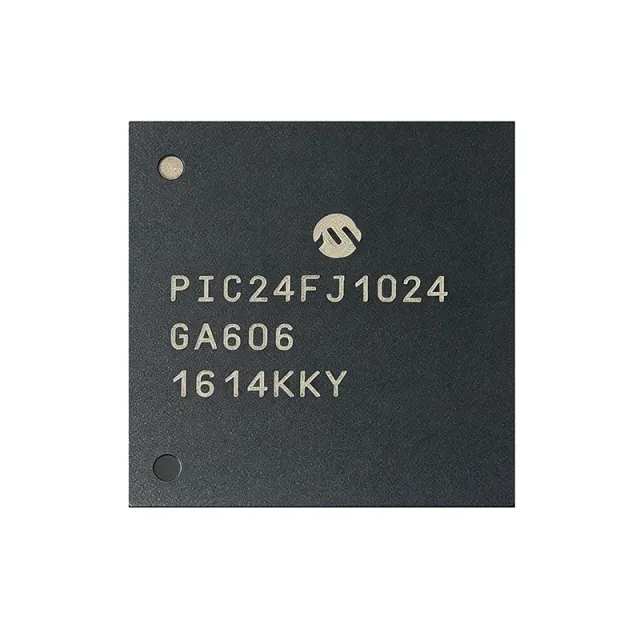
The Microchip Technology PIC24FJ1024GA606-E/MR is a 16-bit RISC microcontroller featuring a PIC24 CPU core operating at up to 32 MHz (16 MIPS), integrating 1 MB of dual-partition Flash program memory with Error Correction Code (ECC) and 32 KB of data RAM, housed in a 64-pin 9 mm x 9 mm QFN (MR) package with an exposed thermal pad. It is part of the eXtreme Low Power PIC24F MCU family, offering a rich peripheral set including 6 UART, 3 SPI, 3 I2C, 2 IrDA, 6 PWM channels, 5 timers, 3 comparators, 8 DMA channels, and 16 analog channels supporting 10/12-bit ADC. A PIC microcontroller (MCU) is a compact, low-cost, programmable processor that integrates a CPU, non-volatile program storage, working RAM, and configurable peripherals onto a single silicon die. The PIC24F family from Microchip extends the 8-bit PIC16/PIC18 architecture into a 16-bit modified-Harvard core, enabling more computational throughput (measured in MIPS) and richer peripherals while preserving the deterministic interrupt model and low-power sleep modes that made the platform popular. PIC MCUs are widely used in industrial sensing, motor control, and consumer devices where ease of development, long product lifecycles, and stable supply matter more than peak raw performance. Key features include dual-bank Flash with live update capability, on-chip ECC for higher reliability, deep sleep currents in the microamp range, and an integrated USB 2.0 full-speed OTG controller. The 16 analog channels are suitable for multi-sensor acquisition boards, while the DMA-driven peripheral set reduces CPU load in data-pump applications. The wide 3.0 V-3.6 V supply range simplifies battery-powered designs and 3.3 V point-of-load architectures. Architecturally, the PIC24FJ1024GA606 uses a 16-bit modified-Harvard core with hardware multiply/divide, a multi-vector interrupt controller, and Microchip's PMM power management unit. The dual-partition Flash supports live update (running one bank while erasing/writing the other), enabling firmware-in-the-field upgrades without service interruption. Peripherals are routed through Microchip's PPS (Peripheral Pin Select) system, allowing flexible assignment of digital functions to most I/O pins. Typical applications include industrial control and HMI panels, low-power IoT sensor nodes, automotive body and accessory ECUs, USB peripherals and embedded host devices, and portable medical instrumentation. For IoT designs, the combination of deep-sleep modes and live-update Flash is especially valuable - nodes can sleep for years on a single battery cell yet receive secure OTA firmware updates in the field. For industrial HMI panels, the 16 analog inputs and graphics-ready PWM timers are well-suited to touch + TFT implementations. When designing with this MCU, pay attention to the PLL configuration sequence and the Vbat/Vddcore/Vddio decoupling layout, since high-speed ADC sampling noise can couple from digital rails. The dual-partition Flash and Live Update flow should be exercised during prototyping; failed live updates can brick the device if the bootloader is not robust. This page synthesizes distributor pricing, drop-in same-package alternatives, and practical design notes not collected in a single place in the manufacturer datasheet.

USD $7.36 In Stock
PIC24FJ1024GA606-E/PT - 16-Bit MCU 1MB Flash 32KB RAM 64-TQFP | Microchip
PIC24FJ1024GA606-E/PT

PIC24FJ1024GA606-E/PT - 16-Bit MCU 1MB Flash 32KB RAM 64-TQFP | Microchip

The Microchip Technology PIC24FJ1024GA606-E/PT is a 16-bit RISC microcontroller featuring a PIC24 CPU core operating at up to 32 MHz, with 1 MB of dual-partition Flash program memory (with ECC) and 32 KB of RAM, housed in a 64-pin TQFP (10x10 mm) package. It belongs to the PIC24F family, which is positioned as an eXtreme Low Power MCU platform for embedded designs requiring large memory and rich connectivity. A PIC24 microcontroller is a 16-bit modified-Harvard architecture MCU built around the PIC instruction set, which sits between 8-bit PIC16/PIC18 parts and the 32-bit PIC32MX/PIC32MZ devices. It belongs to the broader category of microcontrollers (MCUs) within the embedded integrated circuit hierarchy: MCU -> microcontroller IC -> embedded processor -> semiconductor. The PIC24F sub-family is engineered for low-power, mixed-signal applications where USB, graphics, and connectivity peripherals are commonly required. Key features of the PIC24FJ1024GA606 include 1 MB Flash (341.5K words x 24 bits) with Error Correction Code, dual-partition memory for Live Update firmware swapping, 32 KB SRAM, 53 general-purpose I/O pins, 12-bit ADC, multiple communication peripherals, and 9 timers with 6 PWM channels and 8 DMA channels. The device is supplied in a -40C to +125C extended temperature grade, suitable for industrial and harsh-environment deployments. Architecturally, the PIC24FJ1024GA606 integrates a wide peripheral set including 3 I2C, 3 SPI, and 6 UART modules, plus dedicated USB and real-time clock peripherals. Live Update dual-partition Flash enables in-field firmware upgrades without downtime, and ECC on Flash ensures reliable operation in safety-conscious applications. The 64-TQFP package (10x10 mm) provides ample I/O count for parallel-bus or display interfaces. Typical applications include industrial control panels, low-power IoT sensor hubs, USB human-interface devices, home appliance control boards, and battery-powered instrumentation where the large 1 MB Flash supports complex protocol stacks (TLS, USB stacks, graphics libraries). When designing with this part, evaluate the actual active-mode current at 32 MHz and the deep-sleep current to size battery budgets. Pin 1 indicator and TQFP-64 footprint are standard, enabling compatibility with existing PIC24FJ Explorer 16 development ecosystems. This page synthesizes distributor pricing, drop-in alternatives within the PIC24FJ family, and practical design notes not found in the manufacturer datasheet.

RFQ Contact
PIC24FJ1024GA606-I/MR - 16-Bit MCU, 1MB Flash, 32KB RAM | Microchip
PIC24FJ1024GA606-I/MR

PIC24FJ1024GA606-I/MR - 16-Bit MCU, 1MB Flash, 32KB RAM | Microchip

The Microchip Technology PIC24FJ1024GA606-I/MR is a 16-bit RISC microcontroller from the PIC24F eXtreme Low Power family, featuring 1MB (341.5K x 24) of dual-partition Flash with ECC and 32KB of SRAM, operating at up to 32MHz in a 64-pin QFN (9x9 mm) package with exposed thermal pad. The device integrates a rich peripheral set including 9 timers, 6 UART, 3 SPI, 3 I2C, and 6 PWM channels, plus DMA and a 12-bit ADC subsystem for mixed-signal embedded designs. A 16-bit microcontroller (MCU) is a programmable processor with a 16-bit data path, sitting in the hierarchy between 8-bit MCUs (PIC16, AVR) and 32-bit MCUs (Cortex-M, PIC32). Within Microchip's portfolio, the PIC24F family targets low-power, deterministic control applications where the simplicity of 8-bit PIC is too constrained but full 32-bit overhead is unnecessary. The PIC24FJ1024GA606 occupies the high-memory tier of this family, where dual-partition Flash and Live Update allow firmware upgrades without halting the application. Key features of this part include eXtreme Low Power (XLP) sleep currents in the microamp range, on-chip ECC for robust code storage, a wide 2.0V to 3.6V operating range, and an integrated LCD driver option for HMI panels. Multiple communication interfaces enable sensor hub, display, and connectivity bridges, while the DMA controller offloads CPU cycles for high-throughput data movement. The 64-QFN exposed-pad package also provides low thermal resistance, supporting industrial temperature operation from -40C to +85C. Architecturally, the PIC24FJ1024GA606 implements a modified Harvard architecture with separate program and data paths, a 16-bit instruction set with 24-bit addressing, and peripheral pin-select (PPS) remapping that decouples peripheral functions from fixed pin assignments. Live Update allows field firmware upgrades by swapping between two Flash partitions, critical for industrial controllers, sensor networks, and remote IoT endpoints where in-service updates are mandatory. Typical applications include industrial IoT sensor nodes, low-power HMI panels with integrated LCD, battery-powered metering and data loggers, building automation controllers, and consumer appliances requiring USB or CAN connectivity via companion transceivers. Designers benefit from Microchip's MPLAB X IDE and Harmony framework, which provide peripheral libraries and code-configurator support that shorten development cycles. When designing with the PIC24FJ1024GA606-I/MR, allocate the exposed pad to a continuous copper pour of at least 1 square inch to manage the small thermal rise and to support reflow soldering. Decouple each VDD/VSS pair with 100nF ceramic capacitors placed within 2mm of the pins, and route the 32.768kHz crystal traces short and guarded to minimize sleep-current drift. For Live Update, follow Microchip application note guidance on dual-partition bootloader placement to avoid accidental overwrites during field upgrades. This page synthesizes distributor pricing, drop-in alternatives, and practical design notes not found in the manufacturer datasheet.

RFQ Contact
PIC24FJ1024GA606T-I/MR - 1MB Flash 16-bit MCU 64-QFN | Microchip
PIC24FJ1024GA606T-I/MR

PIC24FJ1024GA606T-I/MR - 1MB Flash 16-bit MCU 64-QFN | Microchip

The Microchip Technology PIC24FJ1024GA606T-I/MR is a 16-bit PIC24F RISC microcontroller featuring a 32 MHz CPU core, 1 MB (341.5K x 24) of dual-partition Flash program memory with Live Update capability, and 32 KB of on-chip SRAM, housed in a 64-pin 9x9 mm QFN package with exposed pad. The device operates from 2.0 V to 3.6 V across an industrial -40C to +85C temperature range and integrates rich peripherals including 3x I2C, 3x SPI, 6x UART, 6x PWM channels, 9 timers, and a 16-channel 12-bit Analog-to-Digital Converter. A microcontroller (microcontroller unit, MCU) is a single-chip computer that integrates a CPU core, non-volatile program memory (Flash), volatile data memory (SRAM), and a wide mix of digital and analog peripherals. Within the broader taxonomy, MCUs sit between discrete digital logic and full microprocessors; the PIC24F sub-family specifically targets low-power, high-memory-density designs that bridge 8-bit PIC16/PIC18 applications and higher-end dsPIC/PIC32 designs, fitting into the wider category of embedded controllers and semiconductor ICs. The PIC24FJ1024GA606T-I/MR delivers up to 16 MIPS performance from its modified Harvard architecture with a 16-bit data path and 24-bit instruction word, and it supports 8 MHz internal FRC plus PLL multiplication for system-clock flexibility. Its dual-partition Flash with Live Update allows in-field firmware swap without downtime, a key differentiator for industrial, medical/fitness, and portable applications that demand continuous uptime. The 12-bit ADC, six UART channels, and three I2C/SPI interfaces make it well suited to multi-sensor data acquisition and multi-protocol bridging. Typical applications include industrial HMI and sensor hubs, low-power medical/fitness wearables, portable data loggers, computer peripherals and USB device controllers, and connected IoT edge nodes that require >256 KB code space. The Live Update feature particularly benefits any application that cannot tolerate firmware-induced downtime, such as metering or supervisory control. Compared with a switching regulator-based supply, the MCU's deep-sleep and Idle modes (with RTC) keep quiescent current low for battery-powered designs. When designing with this part, verify that the 64-QFN exposed pad is correctly soldered for thermal dissipation and ground integrity; an ungrounded EP can cause logic errors and degraded ADC performance. Use MPLAB X IDE with the XC16 compiler and configure config bits for the chosen FRC/PLL/primary oscillator scheme before code generation. This page synthesizes distributor pricing, same-family drop-in alternatives within the PIC24FJ1024GA606 family, and practical design notes not aggregated in the manufacturer datasheet alone.

RFQ Contact
PIC24FJ1024GA606T-I/PT - 1MB Flash 16-bit MCU 32MHz TQFP-64 | Microchip
PIC24FJ1024GA606T-I/PT

PIC24FJ1024GA606T-I/PT - 1MB Flash 16-bit MCU 32MHz TQFP-64 | Microchip

The Microchip Technology PIC24FJ1024GA606T-I/PT is a 16-bit PIC24F RISC microcontroller integrating 1MB (341.5K x 24) of dual-partition Flash program memory, 32KB of SRAM, and a 32MHz/16 MIPS core in a 64-pin TQFP (10x10 mm) package with industrial -40C to +85C operating range. Tape-and-reel packaging is indicated by the "T" suffix. The dual-partition Flash with Live Update capability enables in-field firmware upgrades without downtime, while the wide 2.0V-3.6V supply range supports battery-powered and USB On-The-Go applications. A microcontroller (MCU) is a single-chip computer integrating a CPU core, non-volatile program memory, working RAM, and peripherals such as timers, ADC, communication controllers, and I/O. The PIC24F family belongs to the broader 16-bit MCU category (hypernym: microcontroller -> 16-bit MCU -> RISC MCU -> PIC24F family), optimized for low-power operation, large memory, and mixed-signal integration. Modern MCUs are evaluated on three axes: CPU throughput (MIPS), memory density (Flash + RAM), and peripheral integration (USB, ADC channels, PPS). Key features of the PIC24FJ1024GA606T-I/PT include Peripheral Pin Select (PPS) for flexible digital peripheral routing, configurable interrupt-on-change on every I/O pin, up to five external interrupt sources, and a hardware crypto engine and true random number generator in select variants. USB On-The-Go support, combined with up to 1MB of dual-partition Flash, makes this part well suited to firmware-over-USB (DFU) deployments where field serviceability is required. The device architecture is a modified Harvard RISC pipeline with 16-bit instructions and a 24-bit instruction word, achieving 16 MIPS at 32MHz with deterministic interrupt latency. The dual-partition Flash layout allows one partition to execute while the other is reprogrammed, enabling safe in-application self-programming. Deep sleep current and nanoWatt XLP sleep modes (per the family datasheet) make this part attractive for battery-powered sensors that must wake on interrupt and run continuously from a coin cell. Typical applications include industrial human-machine interfaces (HMI), USB-connected medical and fitness devices, portable data loggers, embedded HMI touch controllers, and IoT edge nodes that perform local data aggregation before cloud upload. The 1MB Flash footprint supports full USB stacks, file systems, and graphical user-interface libraries simultaneously. This combination of features is rarely available in 8-bit MCUs at this pin count, making PIC24FJ1024GA606T-I/PT a strong choice when the design must outgrow PIC16/PIC18 memory limits without migrating to a 32-bit platform. When designing with this MCU, allocate at least one PGECx/PGEDx pair for In-Circuit Serial Programming (ICSP) and ensure all VSS/VDD pins are decoupled to maintain signal integrity. Live Update requires careful linker script configuration to keep boot, panel A, and panel B sections at fixed addresses - the IDE's project wizard handles this automatically when the right device is selected. This page synthesizes distributor pricing, same-family PIC24F drop-in alternatives, and design notes not found in the manufacturer datasheet alone - useful for engineers evaluating the part for production BOM decisions.

RFQ Contact
PIC24FJ1024GA610-E/BG - 16-Bit MCU, 1MB Flash, 32MHz, 121-TFBGA | Microchip
PIC24FJ1024GA610-E/BG

PIC24FJ1024GA610-E/BG - 16-Bit MCU, 1MB Flash, 32MHz, 121-TFBGA | Microchip

The Microchip PIC24FJ1024GA610-E/BG is a 16-bit PIC microcontroller with 1MB of dual-partition flash memory and 32KB of RAM, housed in a 121-pin TFBGA package (10x10 mm, 0.8 mm pitch). Operating from 2.0V to 3.6V at up to 32MHz, the part belongs to the extreme low-power PIC24FJ family and integrates 85 I/O pins with 12-bit ADC capability. A microcontroller (MCU) is a single-chip computer that combines a CPU core, program memory, data RAM, and peripheral interfaces (ADC, timers, communication ports) in one package. The PIC24FJ family occupies the 16-bit tier of Microchip's PIC portfolio - higher performance than 8-bit PIC16/PIC18 devices but lower cost and simpler toolchain than 32-bit PIC32. Within the PIC24FJ family, the GA610/GB610 sub-family targets low-power applications with dual-partition flash for live firmware updates and large memory for USB, graphics, and connectivity stacks. Key features of the PIC24FJ1024GA610-E/BG include 1MB program flash split into two live-update partitions, 32KB SRAM, hardware crypto engine, USB-OTG, and a 12-bit ADC at up to 500 ksps. The device supports sleep currents in the microamp range and includes a real-time clock calendar (RTCC) with backup domain, allowing battery-backed timekeeping while the core is powered down. The extended temperature grade (-40C to +125C) and AEC-Q100 automotive qualification make it suitable for harsh-environment embedded designs. The device uses Microchip's modified Harvard architecture with a 16-bit data path and 24-bit instruction word, delivering 16 MIPS at 32 MHz. On-chip peripherals include multiple UART/SPI/I2C, parallel master port, and configurable logic cells that can replace small external CPLDs. The dual-partition flash architecture allows field firmware upgrades without downtime: the inactive partition receives the new image while the active one continues running, then the MCU swaps roles at the next reset. Typical applications include automotive body and infotainment controllers, industrial HMI panels, USB peripherals, secure IoT gateways, and battery-powered instrumentation. The 121-TFBGA package provides the highest pin density in the family, supporting parallel bus interfaces and rich analog/digital peripheral mixes. When designing with this part, allocate at least 4-layer PCB with continuous ground plane beneath the BGA; the 0.8 mm pitch requires NSMD pads and microvia-in-pad for reliable assembly. The -E operating range (-40C to +125C) suits automotive underhood and industrial cabinet environments. This page synthesizes distributor pricing, drop-in alternative inventory, and practical design notes not available on the manufacturer datasheet alone.

RFQ Contact
PIC24FJ1024GA610-E/PT - 16-Bit MCU 1MB Flash 100-TQFP | Microchip
PIC24FJ1024GA610-E/PT

PIC24FJ1024GA610-E/PT - 16-Bit MCU 1MB Flash 100-TQFP | Microchip

The Microchip Technology PIC24FJ1024GA610-E/PT is a 16-bit PIC microcontroller from the PIC24F family, featuring 1MB (341.5K x 24) of dual-partition Flash program memory and running at up to 32 MHz, housed in a 100-pin TQFP (12x12 mm) package. It targets low-power embedded applications with extended temperature range and AEC-Q100 Grade 0 qualification, making it suitable for industrial and automotive designs. The device operates from a 2.0V to 3.6V supply with on-board voltage regulation supporting 3.3V system rails. A 16-bit microcontroller (MCU) is a programmable processor with a 16-bit data path, 16-bit registers, and 16-bit ALU, sitting in the taxonomy: MCU -> microcontroller -> embedded processor -> semiconductor. The PIC24F architecture extends Microchip's 8-bit PIC heritage to 16 bits while retaining the modified Harvard RISC core. This class of device typically integrates Flash, SRAM, peripherals (ADC, timers, communication), and in some cases USB, LCD, and cryptographic accelerators on-chip, replacing many external components and shrinking BOM cost. Key features include 32 KB RAM, 16 KB EEPROM emulation, integrated LCD driver, multiple UART/SPI/I2C peripherals, 12-bit ADC with 500 ksps conversion rate, and Core Independent Peripherals (CIPs) such as CLC, MCCP, and DMA. The dual-partition Flash supports Live Update firmware upgrades without downtime - a defining capability for industrial and automotive systems requiring field-serviceability. Sleep current is rated at tens of microamperes with retention RAM. Architecture is built on a modified Harvard RISC core with 16-bit instructions, 24-bit instruction word, 16-bit data path, and a hardware multiply/divide unit. The on-chip voltage regulator provides 1.8V/1.2V core rails from a single 3.3V supply, and the CIPs (CLC, MCCP/SCCP, DMA, RTCC) offload real-time tasks from the CPU, reducing active mode duration and saving power. Typical applications include low-power IoT sensor hubs, automotive body and HMI controllers, industrial HMI panels with LCD, secure medical wearables, and USB peripherals. Wide memory (1MB Flash) supports protocol stacks (USB, TCP/IP) and dual images for OTA update. Design tip: verify AEC-Q100 grade in the part suffix (E vs -ED). The /PT suffix denotes TQFP-100. Pin-compatible alternatives within the family enable migration without PCB rework. This page synthesizes distributor pricing, same-family drop-in alternatives, and practical design notes not consolidated in the manufacturer datasheet alone.

RFQ Contact