Power Management
Subcategories
Products (2,800+)

L99LD21 - Automotive High Power LED Driver | STMicroelectronics
The L99LD21 is an automotive-grade, high-power LED driver from STMicroelectronics, specifically designed to control two independent high-brightness LED strings for automotive front lighting applications. It integrates a boost controller with a high-side current source, enabling efficient and precise current regulation for LED strings with forward currents up to 1.5 A (average) and forward voltages up to 50 V. The device operates from a wide battery voltage range of 5.5 V to 24 V and is load dump protected, making it suitable for both 12 V and 24 V automotive electrical systems. An LED driver is a power management IC that regulates the current flowing through one or more LEDs to ensure consistent brightness and protect the LEDs from current-induced damage. In automotive lighting, LED drivers are essential for headlamps, daytime running lights, and interior lighting, where they convert the vehicle's battery voltage into a controlled current source. The L99LD21 belongs to the family of automotive LED drivers, which are part of the broader power management IC category, and are designed to meet stringent automotive reliability standards such as AEC-Q100. Key features of the L99LD21 include a wide input voltage range, high output current capability, and integrated protection features such as over-temperature and over-voltage protection. The device supports PWM dimming for brightness control and includes a fault diagnostic output for system monitoring. Its high efficiency reduces power dissipation, which is critical in thermally constrained automotive environments. The device is AEC-Q100 qualified, ensuring reliability for automotive applications. The L99LD21 uses a boost converter topology to step up the battery voltage to the level required by the LED string, while the integrated high-side current source regulates the LED current with high accuracy. This architecture minimizes external component count and simplifies PCB layout. The device is available in a compact QFN40L 6x6 package with wettable flanks and exposed pad, suitable for space-constrained automotive modules. It also features ST SPI communication v4.1, a timeout watchdog, and a limp home function for enhanced safety. Typical applications include automotive headlamps, daytime running lights, fog lamps, and interior ambient lighting. The device's robust design and automotive qualification make it suitable for use in harsh environments with wide temperature variations and electrical transients. The L99LD21 is also available as an evaluation board (L99LD21-ADIS) for development and testing. When designing with the L99LD21, it is important to ensure proper thermal management and to select external components that meet the device's specifications. The PWM dimming input allows for flexible brightness control, and the fault output can be used to implement diagnostic functions in the vehicle's lighting control unit. The device's low standby current helps reduce power consumption when the lighting system is not in use.

L99MOD53XPTR - Multi-Channel MOSFET Driver | STMicroelectronics
The L99MOD53XPTR is a multi-channel MOSFET driver IC from STMicroelectronics, designed for automotive and industrial applications requiring high-side and low-side driver configurations. It integrates multiple channels with built-in protection features, making it suitable for driving resistive, inductive, and capacitive loads. The device operates over a wide supply voltage range and provides diagnostic feedback for fault detection. A MOSFET driver is a power management IC that translates low-power control signals from a microcontroller into high-current, high-voltage signals capable of driving the gate of power MOSFETs. In the hierarchy of power management, a MOSFET driver sits between the logic controller and the power stage, ensuring efficient switching and protection. The L99MOD53XPTR belongs to the family of smart power drivers, which integrate protection, diagnostics, and control logic on a single chip. Key features of the L99MOD53XPTR include multiple output channels, each capable of driving external N-channel MOSFETs, with programmable current control and diagnostic functions. It supports a supply voltage range of [DATA_NEEDED: supply voltage range] and offers overcurrent, overtemperature, and short-circuit protection. The device is available in a [DATA_NEEDED: package type] package, suitable for surface-mount assembly. The L99MOD53XPTR utilizes a robust architecture with integrated charge pumps and level shifters to drive high-side MOSFETs. It communicates with the host microcontroller via a serial peripheral interface (SPI), enabling real-time monitoring and control. The device is designed to meet automotive-grade requirements, including AEC-Q100 qualification, ensuring reliable operation in harsh environments. Typical applications include automotive body control modules, LED lighting control, DC motor control, and solenoid drivers. In automotive body control, the L99MOD53XPTR can drive multiple loads such as relays, bulbs, and motors, with diagnostic feedback for fault detection. In industrial automation, it provides a flexible solution for driving various actuators and valves. When designing with the L99MOD53XPTR, ensure proper thermal management by providing adequate PCB copper area for heat dissipation. The SPI interface allows configuration of output current limits and fault handling, which should be set according to the load requirements. Additionally, consider the supply voltage range and ensure it matches the application's power rail.
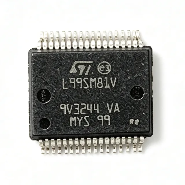
L99SM81V - Automotive Stepper Motor Driver | STMicroelectronics
The L99SM81V is an automotive-grade integrated driver for bipolar two-phase stepper motors, designed by STMicroelectronics for precise current-controlled micro-stepping with programmable amplitude. It integrates a microstepping controller with a power stage capable of driving up to 1.2 A per phase, and operates from a supply voltage range of 6 V to 28 V, making it suitable for direct connection to automotive battery rails. The device is available in a 40-pin QFN (6x6 mm) package and is AEC-Q100 qualified for automotive applications. A stepper motor driver is a power management IC that converts digital step and direction commands into the precise current sequences needed to rotate a stepper motor in controlled increments. It sits between a microcontroller and the motor, translating low-power logic signals into high-current drive signals. In the system hierarchy, a stepper motor driver is a type of motor driver, which falls under power management ICs, which are part of the broader category of analog and mixed-signal semiconductors. Key features of the L99SM81V include a programmable microstepping resolution up to 1/16 step, integrated current sensing with no external sense resistors, and a SPI interface for configuration and diagnostics. It also features overcurrent, overtemperature, and undervoltage protection, along with a low quiescent current in standby mode, which is critical for automotive battery conservation. The device is AEC-Q100 qualified, ensuring reliability across the -40°C to +150°C junction temperature range. The L99SM81V uses a proprietary current-control architecture that combines a constant-current chopper with a programmable decay mode, enabling smooth and quiet motor operation. The integrated current sensing eliminates the need for external sense resistors, reducing BOM cost and PCB area. The SPI interface allows real-time monitoring of fault conditions and precise adjustment of motor parameters, making it a flexible solution for complex automotive motion control. Typical applications include headlamp leveling systems, where precise positioning is required for optimal beam alignment, HVAC flap control for cabin comfort, and instrument cluster stepper motors for gauge indication. The wide supply voltage range and robust protection features make it ideal for direct battery connection in 12 V automotive systems. When designing with the L99SM81V, ensure adequate PCB copper area for thermal dissipation, especially when driving high currents continuously. The SPI interface should be isolated from high-current traces to minimize noise coupling. Proper decoupling capacitors on the supply pins are essential to maintain stable operation during motor transients.
LC4136C-X2T - LED Driver IC | onsemi | Display Backlight
The onsemi LC4136C-X2T is an LED driver integrated circuit offered for display-backlight and general LED-driving applications, with the verified source identifying it as an LED driver and interface IC. Its exact electrical ratings, pin configuration, package dimensions, operating limits, and protection features were not included in the supplied web data, so those values remain unavailable rather than being inferred. The verified distributor records identify LC4136C-X2T by onsemi and associate it with driver, receiver, transceiver, and display-driver listings. An LED driver is a power-management or interface IC that regulates current or voltage delivered to one or more LEDs. In display equipment, the driver establishes the electrical operating point of backlight LEDs, helping maintain illumination while protecting the light source from excessive current. The LC4136C-X2T is consequently positioned for circuits where an LED load is controlled from an electronic system rather than directly from a supply rail. The available evidence does not establish whether this part uses constant-current or constant-voltage regulation, how many LED channels it provides, or whether it includes PWM dimming. It also does not confirm a manufacturer datasheet URL. Those omissions prevent a safe characterization of output-current tolerance, switching frequency, efficiency, dimming ratio, thermal resistance, or maximum LED-string voltage. Engineers should obtain the official onsemi technical documentation before selecting it for a new design. Typical use cases suggested by the verified LED-driver classification include LCD backlight control, panel illumination, indicator lighting, and compact display modules. These are application categories rather than confirmed manufacturer reference designs. Actual suitability depends on the unavailable voltage range, current capability, channel count, pinout, and package data, as well as the LED string topology used in the target board. Before designing around LC4136C-X2T, verify the manufacturer datasheet, compare every electrical limit against the intended LED string, and confirm that the PCB land pattern matches the required package. Do not substitute a similarly named LC4136 variant without checking pin functions and ratings. The verified LCSC listing reports a price from $0.4707, while other distributor records report $1.16 and $1.33, showing meaningful source and quantity variation. This page consolidates the supplied distributor identity, pricing, stock, and cross-reference evidence while separating verified facts from missing technical information. It is intended to support initial sourcing and comparison, not to substitute for the complete manufacturer datasheet, PCB footprint, or application validation.

LC709209FXE-01TBG - 1-Cell Li-Ion Fuel Gauge | onsemi
The onsemi LC709209FXE-01TBG is a battery fuel gauge IC for 1-cell lithium-ion and lithium-polymer batteries, communicating over an I2C serial interface and housed in a 12-ball WLCSP package measuring 1.48 x 1.91 mm. It belongs to onsemi's Smart LiB Gauge family of fuel gauges. A battery fuel gauge is a power-management IC that estimates the state of charge (SOC) of a rechargeable cell and reports it to a host microcontroller. Within the power-management hierarchy, the fuel gauge sits alongside chargers and protectors in the battery management IC category, converting cell voltage and current behavior into a usable percentage readout. Accurate gauging is essential in portable systems because cell voltage alone is a poor predictor of remaining capacity, especially across different battery chemistries and load profiles. Key features of the LC709209FXE include its dedicated 1-cell Li-ion/Li-polymer support, I2C digital interface for host communication, ultra-compact 12-WLCSP (1.48 x 1.91 mm) footprint suited to space-constrained wearables and IoT devices, and Pb-free and halogen-free construction per the onsemi data sheet. The device is supplied in tape and reel packaging (refer to onsemi BRD8011/D for tape and reel specifications). From a technical perspective, the Smart LiB Gauge architecture performs SOC estimation based on cell voltage monitoring with profile-based algorithms, requiring minimal external components. Because it gauges by voltage, integration into a design is straightforward: connect the cell voltage sense line, the I2C bus, and the supply rails. Host software reads SOC values through the I2C register map, allowing firmware-level power management decisions such as low-battery shutdown or capacity reporting to an operating system. Typical applications include true wireless stereo (TWS) earbuds, smartwatches and fitness bands, small IoT sensor nodes, and other single-cell portable products where board area is at a premium and battery life reporting is a user-facing feature. When designing with this part, verify the I2C address and pull-up resistor sizing against the host bus loading, and confirm the battery profile matches the cell chemistry in use, since gauging accuracy depends on correct cell characterization. This page synthesizes distributor pricing, availability, cross-reference findings, and practical design notes not consolidated in the manufacturer data sheet, with pricing verified as of 2026-09-13.
LC709209FXE-01TBG - 1-Cell Li-Ion Fuel Gauge | onsemi
The onsemi LC709209FXE-01TBG is a battery fuel gauge IC for 1-cell lithium-ion and lithium-polymer packs, housed in a 12-ball WLCSP package measuring just 1.48 x 1.91 mm. It measures battery voltage and reports state-of-charge over an I2C serial interface, making it one of the most compact smart-gauge solutions for space-constrained portable designs. A battery fuel gauge is a power-management IC that estimates the remaining capacity of a rechargeable battery. Within the power management IC hierarchy, it sits alongside battery chargers and protectors, but its role is measurement rather than energy transfer: it translates cell voltage, and in this family internal modeling, into a percentage-of-full-charge value a host microcontroller can read. Gauges are essential in any product where accurate runtime indication or low-battery warnings matter. Key features of the LC709209F family include ultra-low power consumption that minimizes drain on the host cell, an I2C-compatible two-wire interface for state-of-charge and status readout, Pb-free and halogen-free construction, and an extremely small 12-WLCSP footprint suited to wearables, true-wireless earbuds, and other handheld electronics. According to the onsemi LC709209F data sheet, the device is specified as a Smart LiB Gauge for 1-cell applications. Technically, the gauge monitors the single-cell pack voltage through an internal ADC path and applies the manufacturer's gauge algorithm to derive state of charge; configuration and status registers are accessible via the I2C bus, allowing the host to read SOC, voltage, and alarm flags and to adjust operating parameters. The WLCSP ball layout keeps external component count minimal, supporting very dense PCB layouts. Typical applications include smartphone and wearable battery monitoring, true-wireless stereo earbud charging cases, portable medical sensors, and IoT asset trackers where a 1-cell Li-ion/Li-polymer pack must be monitored with minimal board area and quiescent drain. Design consideration: WLCSP devices require careful PCB land-pattern design per the manufacturer's packaging specification, and the I2C bus should include appropriate pull-up resistors sized for the chosen bus speed. This page adds distributor pricing, cross-reference data, and application guidance not consolidated in the manufacturer data sheet.

LD1117ADJTR - 1A Low Dropout Positive Regulator | STMicroelectronics
The STMicroelectronics LD1117ADJTR is a low dropout positive voltage regulator capable of delivering up to 1A of output current. It features an adjustable output voltage range from 1.25V to 15V, with a typical dropout voltage of 1.1V at 1A load. The device is available in the SOT-223 package, which is widely used for surface-mount applications. Data verified as of 2026-08-05. A low dropout regulator (LDO) is a type of linear voltage regulator that maintains a stable output voltage even when the input voltage is very close to the output voltage. LDOs are essential in power management systems where a clean, regulated supply is needed with minimal voltage headroom. They are part of the voltage regulator family, which also includes switching regulators, and are widely used in battery-powered devices, automotive electronics, and industrial control systems. Key features of the LD1117ADJTR include a fixed or adjustable output, internal current limiting, and thermal shutdown protection. The device operates over a junction temperature range of 0°C to 125°C, making it suitable for a variety of environments. The SOT-223 package offers a compact footprint with a thermal pad for improved heat dissipation, enabling reliable operation at moderate power levels. The LD1117ADJTR uses a PNP pass transistor architecture, which provides low dropout voltage and stable operation. The adjustable version uses an external resistor divider to set the output voltage, allowing flexibility in design. The device also features a low quiescent current, which is beneficial for battery-powered applications where power efficiency is critical. Typical applications include post-regulation for switching power supplies, battery chargers, and as a local supply for microcontrollers and other digital ICs. The wide input voltage range and low dropout make it ideal for automotive and industrial applications where input voltage can vary significantly. When designing with the LD1117ADJTR, ensure adequate input-to-output voltage headroom to maintain regulation. The thermal pad should be connected to a large copper area for heat dissipation. Proper decoupling capacitors on input and output are essential for stability and transient response. This page synthesizes distributor pricing, drop-in alternatives, and practical design notes not found in the STMicroelectronics datasheet, providing a comprehensive resource for engineers.

LD1117ADT18TR - 1.8V Fixed 800mA LDO Regulator | STMicroelectronics
The LD1117ADT18TR is a low-dropout linear regulator from STMicroelectronics, providing a fixed 1.8V output with a maximum output current of 800mA. It is housed in a DPAK (TO-252) surface-mount package, designed for a wide range of applications requiring a stable and low-noise power supply. The device operates with an input voltage range up to 15V and features a typical dropout voltage of 1.1V at 800mA load, making it suitable for battery-powered and industrial systems. A low-dropout regulator (LDO) is a type of linear voltage regulator that maintains a constant output voltage even when the input voltage is only slightly higher than the output. Unlike switching regulators, LDOs provide a clean, noise-free output, making them ideal for analog and RF circuits. In the hierarchy of power management, an LDO is a linear regulator, which is a type of voltage regulator, which falls under power management ICs, which are part of the broader semiconductor category. The LD1117ADT18TR is a fixed-output LDO, simplifying design by eliminating the need for external resistor dividers. Key features of the LD1117ADT18TR include a fixed 1.8V output, 800mA output current capability, and a dropout voltage of 1.1V typical at full load. It also offers internal current limiting and thermal shutdown protection, ensuring safe operation under fault conditions. The device is available in the DPAK package, which provides good thermal performance with a junction-to-ambient thermal resistance of 100°C/W, allowing for moderate power dissipation without external heatsinks. The LD1117ADT18TR is built on a robust bipolar process, providing excellent line and load regulation. It is designed to be stable with low-ESR ceramic capacitors, making it easy to use in modern designs. The device also features a wide operating temperature range of -40°C to +125°C, suitable for industrial and automotive environments. Typical applications include powering microcontrollers, FPGAs, and other digital ICs that require a 1.8V rail, as well as providing a clean supply for analog circuits such as op-amps and ADCs. It is also used in battery-powered devices, where its low dropout voltage maximizes battery life. When designing with the LD1117ADT18TR, ensure that the input voltage is at least 1.1V above the output voltage to maintain regulation. Use a 10µF output capacitor to ensure stability, and place it close to the output pin. The thermal pad of the DPAK package should be connected to a large copper area for effective heat dissipation.
LD1117ADT33TR - 3.3V Fixed 800mA LDO Regulator | STMicroelectronics
The STMicroelectronics LD1117ADT33TR is a low-dropout (LDO) linear voltage regulator providing a fixed 3.3V output with a maximum output current of 800mA. It is housed in a DPAK (TO-252) surface-mount package, designed for a wide range of consumer, industrial, and computing applications. The device operates with an input voltage range from 4.75V to 15V, making it suitable for 5V and 12V rails. An LDO (Low-Dropout) linear regulator is a type of voltage regulator that maintains a stable output voltage even when the input voltage is very close to the output voltage. Unlike standard linear regulators, LDOs use a pass transistor operating in the saturation region, allowing a low dropout voltage. In the system hierarchy, an LDO is a linear regulator, which is a type of voltage regulator, which falls under power management ICs, which are semiconductors. This hierarchy is essential for understanding where the LD1117ADT33TR fits in power management design. Key features of the LD1117ADT33TR include a dropout voltage of typically 1.1V at 800mA load, a quiescent current of 5mA, and a line regulation of 0.2% (typical). It also offers thermal shutdown and internal current limiting, providing robust protection for the load. The fixed 3.3V output eliminates the need for external resistor dividers, simplifying design and reducing component count. The LD1117ADT33TR is built on a bipolar process, offering low noise and fast transient response. The DPAK package provides a thermal resistance of 50°C/W (junction-to-ambient), allowing moderate power dissipation without a heatsink. The device is RoHS compliant and lead-free, meeting modern environmental standards. Typical applications include powering microcontrollers, FPGAs, and digital logic in embedded systems, as well as providing a clean 3.3V rail for sensors and interface circuits. It is also used in set-top boxes, routers, and other consumer electronics where a stable 3.3V supply is required. When designing with the LD1117ADT33TR, ensure adequate input-output voltage headroom to maintain regulation. A minimum input voltage of 4.75V is required for 3.3V output. Use a 10µF output capacitor for stability, and place it close to the output pin. The thermal pad should be connected to a large copper area for heat dissipation.
LD1117DT33TR - 800mA Low Dropout Voltage Regulator | STMicroelectronics
The STMicroelectronics LD1117DT33TR is a low dropout positive voltage regulator providing a fixed 3.3V output with a maximum output current of 800mA. It is available in the SOT-223 package, which is suitable for surface mount applications. The device features a dropout voltage of typically 1.1V at 800mA load, making it efficient for battery-powered and low-headroom applications. A low dropout regulator (LDO) is a type of linear voltage regulator that can maintain a stable output voltage even when the input voltage is very close to the output voltage. LDOs are essential in power management systems where noise-sensitive analog circuits require clean, ripple-free power rails. They are part of the voltage regulator family, which also includes switching regulators, and are widely used in consumer electronics, industrial controls, and automotive systems. Key features of the LD1117DT33TR include a fixed 3.3V output, 800mA output current capability, internal current limiting, and thermal shutdown protection. The device operates over a junction temperature range of -40°C to +125°C, ensuring reliable performance in harsh environments. The SOT-223 package offers a compact footprint with a thermal pad for improved heat dissipation. The LD1117DT33TR utilizes a PNP pass transistor architecture, which provides low dropout voltage and stable operation. The internal bandgap reference ensures accurate output voltage regulation across temperature and load variations. The device is designed for simplicity, requiring only two external capacitors for stability, making it easy to integrate into various designs. Typical applications include powering microcontrollers, FPGA core voltages, and analog sensor interfaces. The fixed 3.3V output is ideal for logic circuits and mixed-signal systems. The low dropout voltage allows operation from a 5V rail with sufficient headroom, making it suitable for 5V to 3.3V conversion in embedded systems. When designing with the LD1117DT33TR, ensure adequate input-to-output voltage headroom to maintain regulation. The input and output capacitors should be placed close to the device pins to minimize parasitic inductance. For high current loads, consider the thermal resistance of the SOT-223 package and provide adequate copper area for heat dissipation.
LD1117S18TR - 1.8V Fixed 800mA LDO Regulator | STMicroelectronics
The STMicroelectronics LD1117S18TR is a low-dropout (LDO) linear voltage regulator providing a fixed 1.8V output with a maximum output current of 800mA. It is housed in a SOT-223 package, which is widely used in surface-mount applications. The device operates with an input voltage range from 2.5V to 15V, making it suitable for a variety of low-voltage power supply applications. An LDO (Low-Dropout) linear regulator is a type of voltage regulator that maintains a stable output voltage even when the input voltage is very close to the output voltage. Unlike standard linear regulators, LDOs can operate with a small dropout voltage, typically less than 1V, which improves efficiency and allows for lower input voltages. In the hierarchy of power management, an LDO is a type of linear regulator, which is a type of voltage regulator, which is a type of power management IC. LDOs are essential in applications where low noise and simplicity are prioritized over efficiency, such as in battery-powered devices and analog circuits. Key features of the LD1117S18TR include a fixed 1.8V output voltage, a dropout voltage of 1.1V at 800mA, and a quiescent current of 5mA. The device also includes internal current limiting and thermal shutdown protection, ensuring safe operation under fault conditions. The SOT-223 package offers a compact footprint with a thermal resistance of 50°C/W, allowing for moderate power dissipation without external heatsinking. The LD1117S18TR is designed with a PNP pass transistor architecture, which provides a low dropout voltage and stable operation. The device is stable with a wide range of output capacitors, including ceramic capacitors, which simplifies the design and reduces component count. The internal current limiting and thermal shutdown features protect the regulator and the load from damage due to overcurrent or overtemperature conditions. Typical applications for the LD1117S18TR include powering microcontrollers, FPGAs, and other digital ICs that require a stable 1.8V supply. It is also used in battery-powered devices, such as portable electronics and IoT devices, where low quiescent current and small size are important. Additionally, the device is suitable for post-regulation in switching power supplies to reduce ripple and noise. When designing with the LD1117S18TR, ensure that the input voltage is at least 1.1V above the output voltage to maintain regulation. The output capacitor should be placed close to the output pin to ensure stability. For higher current applications, consider the power dissipation and use appropriate PCB copper area to keep the junction temperature within safe limits.
LD1117S25TR - 800mA Low Dropout Positive Regulator | STMicroelectronics
The LD1117S25TR is a low dropout positive voltage regulator from STMicroelectronics, designed to deliver a fixed 2.5V output with a maximum output current of 800mA. It is available in the SOT-223 package, which is suitable for surface-mount applications requiring efficient thermal performance. The device operates with an input voltage range up to 15V and features a typical dropout voltage of 1.1V at 800mA load, making it ideal for battery-powered and low-voltage systems. A low dropout regulator (LDO) is a type of linear voltage regulator that maintains a stable output voltage even when the input voltage is only slightly higher than the output. Unlike standard linear regulators, LDOs achieve a low dropout voltage by using a PNP pass transistor or a PMOS device, allowing them to operate efficiently in applications where the input-to-output voltage difference is small. LDOs are a subset of linear regulators, which in turn are part of the broader category of voltage regulators within power management integrated circuits (ICs). Key features of the LD1117S25TR include a fixed 2.5V output, a maximum output current of 800mA, and a dropout voltage of 1.1V at full load. The device also offers internal current limiting and thermal shutdown protection, ensuring safe operation under fault conditions. The SOT-223 package provides a compact footprint with a thermal resistance of approximately 50°C/W, enabling moderate power dissipation without external heatsinking. The LD1117S25TR utilizes a PNP pass transistor architecture, which allows for low dropout operation and stable output with a minimum output capacitor of 10µF. The device is designed to be stable with tantalum or aluminum electrolytic capacitors, and it includes a bandgap reference for accurate output voltage regulation. The internal current limit and thermal shutdown circuits protect the device from overcurrent and overtemperature conditions, enhancing system reliability. Typical applications for the LD1117S25TR include post-regulation for switching power supplies, battery-powered equipment, and low-voltage logic supplies. Its fixed 2.5V output is commonly used to power microcontrollers, memory ICs, and other digital circuits that require a stable 2.5V rail. The low dropout voltage and low quiescent current make it suitable for portable devices where power efficiency is critical. When designing with the LD1117S25TR, ensure that the input voltage is at least 1.1V above the output voltage to maintain regulation. The output capacitor should be placed close to the output pin to minimize parasitic inductance and ensure stability. Additionally, the thermal pad of the SOT-223 package should be connected to a copper area on the PCB to improve heat dissipation.
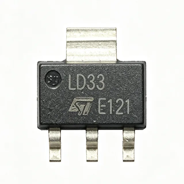
LD1117S33TR - 800mA Low Dropout Positive Regulator | STMicroelectronics
The STMicroelectronics LD1117S33TR is a low dropout positive voltage regulator providing a fixed 3.3V output with a maximum output current of 800mA. It is available in the SOT-223 package, designed for surface mount applications. The device operates with an input voltage range up to 15V and features a typical dropout voltage of 1.1V at 800mA load. Data verified as of 2026-08-05. A low dropout regulator (LDO) is a type of linear voltage regulator that can maintain a stable output voltage even when the input voltage is very close to the output voltage, minimizing power dissipation. LDOs are essential in power management ICs, providing clean, low-noise supply rails for sensitive analog and digital circuits. The LD1117S33TR belongs to the LD1117 family, which includes adjustable and fixed output versions, and is widely used in consumer, industrial, and automotive applications. Key features of the LD1117S33TR include a fixed 3.3V output, 800mA output current capability, internal current limiting, and thermal shutdown protection. The device offers a typical dropout voltage of 1.1V at full load, ensuring efficient operation even with low input-to-output voltage margins. The SOT-223 package provides a compact footprint with a thermal pad for improved heat dissipation, making it suitable for space-constrained designs. The LD1117S33TR utilizes a PNP pass transistor architecture, which allows for low dropout operation and stable performance across a wide range of load currents. The internal current limiting and thermal shutdown features protect the device and the load from fault conditions. The device is stable with low ESR ceramic capacitors, simplifying the external component count and reducing board space. Typical applications include post-regulation for switching power supplies, battery-powered equipment, and as a local supply rail for microcontrollers, FPGAs, and analog circuits. The fixed 3.3V output is ideal for powering 3.3V logic and mixed-signal systems. The wide input voltage range and robust protection features make it suitable for industrial control systems and consumer electronics. When designing with the LD1117S33TR, ensure adequate input-to-output voltage headroom to maintain regulation under all load conditions. The dropout voltage increases with load current, so a minimum input voltage of 4.4V is recommended for a 3.3V output at 800mA. Proper PCB layout with adequate copper area for heat dissipation is essential for reliable operation at high load currents. This page synthesizes distributor pricing, drop-in alternatives, and practical design notes not found in the STMicroelectronics datasheet, providing engineers with a comprehensive resource for selecting and implementing the LD1117S33TR.
LD1117S50TR - 800mA Low Dropout Positive Regulator | STMicroelectronics
The LD1117S50TR is a low dropout positive voltage regulator from STMicroelectronics, designed to deliver a fixed 5.0V output with a maximum output current of 800mA. It is available in the SOT-223 package, which is a surface-mount package with an exposed tab for enhanced thermal performance. The device operates with an input voltage range from 6.5V to 15V, making it suitable for a variety of applications that require a stable 5V rail. A low dropout (LDO) regulator is a type of linear voltage regulator that can maintain a regulated output voltage even when the input voltage is very close to the output voltage. This is achieved by using a pass transistor that operates in the saturation region, minimizing the voltage drop across the regulator. LDO regulators are essential in power management systems where efficiency and noise are critical, such as in battery-powered devices, automotive electronics, and industrial control systems. They are part of the broader category of voltage regulators, which also includes switching regulators and charge pumps, each with distinct trade-offs in efficiency, noise, and complexity. Key features of the LD1117S50TR include a low dropout voltage of 1.1V at 800mA, a typical quiescent current of 5mA, and a load regulation of 0.2% typical. The device also includes internal current limiting and thermal shutdown protection, ensuring safe operation under fault conditions. The SOT-223 package offers a thermal resistance of 50°C/W (junction-to-ambient), allowing for moderate power dissipation without external heatsinking in many applications. The LD1117S50TR utilizes a PNP pass transistor architecture, which provides a low dropout voltage and stable operation. The internal bandgap reference ensures accurate output voltage regulation across temperature and load variations. The device is designed to be stable with a wide range of output capacitors, including ceramic capacitors, which simplifies the design and reduces the overall solution size. Typical applications include post-regulation of switching power supplies, battery-powered equipment, and as a local 5V rail for microcontrollers, sensors, and analog circuits. The fixed 5V output is ideal for logic circuits and USB-powered devices. The low dropout voltage allows efficient operation even when the input voltage is only slightly above the output, maximizing battery life in portable applications. When designing with the LD1117S50TR, it is important to ensure adequate input-to-output voltage headroom to maintain regulation under all load conditions. The input and output capacitors should be placed close to the device pins to minimize parasitic inductance and ensure stability. The exposed tab of the SOT-223 package should be connected to a copper pour to enhance thermal dissipation, especially when operating at high load currents.

LD39015M33R - 150mA, 3.3V Ultra-Low Noise LDO | STMicroelectronics
The STMicroelectronics LD39015M33R is a fixed 3.3V output, ultra-low noise, low-dropout linear regulator capable of delivering up to 150mA of output current. It is housed in a compact SOT-23-5 package, making it ideal for space-constrained portable and battery-powered applications. The device operates over an input voltage range of 1.5V to 5.5V, with a typical dropout voltage of only 100mV at 150mA load, ensuring efficient operation even with minimal input-to-output headroom. An LDO (Low-Dropout) linear regulator is a type of voltage regulator that maintains a stable output voltage even when the input voltage is very close to the output voltage. Unlike standard linear regulators that require a larger dropout voltage, LDOs use a pass transistor operating in the saturation region to achieve low dropout, making them essential in battery-powered devices where maximizing usable battery voltage is critical. In the power management hierarchy, an LDO is a type of linear regulator, which is a subset of voltage regulators, which in turn are key components of power management ICs (PMICs) used across virtually all electronic systems. Key features of the LD39015M33R include an ultra-low output noise of 30uVrms (typical) over a 10Hz to 100kHz bandwidth, a high power supply rejection ratio (PSRR) of 60dB at 1kHz, and a low quiescent current of 40uA (typical). The device also incorporates internal current limiting and thermal shutdown protection, ensuring robust operation under fault conditions. The fixed 3.3V output eliminates the need for external resistor dividers, simplifying design and reducing component count. Technically, the LD39015M33R is built on a CMOS process, which contributes to its low quiescent current and low dropout performance. The internal bandgap reference provides a stable 3.3V output with an accuracy of ±2% over the full operating temperature range of -40°C to +125°C. The device is stable with ceramic output capacitors as low as 1uF, allowing for compact and cost-effective designs. The SOT-23-5 package has a thermal resistance (theta_JA) of approximately 250°C/W, which must be considered for power dissipation in high-temperature environments. Typical applications include powering low-power microcontrollers, wireless modules (such as Bluetooth Low Energy and Zigbee), MEMS sensors, and other analog/RF circuits that require a clean, stable 3.3V supply. The ultra-low noise and high PSRR make it particularly suitable for noise-sensitive applications like audio codecs and RF transceivers, where supply noise can degrade performance. When designing with the LD39015M33R, ensure that the input voltage remains above the dropout voltage plus the output voltage (3.3V + 100mV = 3.4V) to maintain regulation. Place a 1uF ceramic capacitor on the input and output as close to the pins as possible. The enable pin (EN) can be used for power sequencing; it is active-high and has an internal pull-down, so it can be left floating to disable the output.

LD39030DTPU33R - 3.3V 300mA Ultra-Low Noise LDO | STMicroelectronics
The STMicroelectronics LD39030DTPU33R is a fixed 3.3V output, 300mA ultra-low-noise LDO linear regulator in a 6-pin UDFN (DFN6) package. It is designed for noise-sensitive applications requiring a clean, stable power rail with minimal external components. The device operates from an input voltage range of 1.5V to 5.5V, making it suitable for battery-powered and low-voltage systems. An LDO (Low-Dropout) linear regulator is a type of voltage regulator that maintains a stable output voltage even when the input voltage is very close to the output voltage. Unlike standard linear regulators, LDOs use a pass transistor with a low saturation voltage, allowing them to operate with a small input-to-output voltage differential. In the system hierarchy, an LDO is a specific type of linear regulator, which is a category of voltage regulator, which in turn is a key component in power management ICs. LDOs are widely used in portable electronics, audio equipment, and RF circuits where low noise and fast transient response are critical. Key features of the LD39030DTPU33R include an ultra-low output noise of 10 uVrms (typical) over a 10 Hz to 100 kHz bandwidth, a high PSRR of 70 dB at 1 kHz, and a low dropout voltage of 120 mV at 300mA load. The quiescent current is only 40 uA, which is ideal for battery-powered applications. The device also includes an enable pin for power sequencing, short-circuit protection, and thermal shutdown. The UDFN-6 package (2mm x 2mm) offers a compact footprint with a thermal resistance of 90 C/W, enabling space-constrained designs. The LD39030DTPU33R uses a CMOS architecture with a precision bandgap reference, achieving excellent line and load regulation. The high PSRR minimizes ripple from upstream switching converters, making it suitable for noise-sensitive analog and RF signal chains. The low quiescent current extends battery life in portable devices, while the enable pin allows for efficient power management in multi-rail systems. Typical applications include audio codec power supplies, RF transceiver power rails, sensor interfaces, and portable medical devices. The wide input range and low dropout voltage also support operation from single-cell Li-ion batteries (3.0V to 4.2V) with adequate headroom. When designing with this device, ensure adequate input-to-output voltage headroom to maintain regulation under all load conditions. The enable pin allows sequential power-up in multi-rail systems, which is essential for processors requiring specific rail sequencing. Place input and output capacitors close to the pins for optimal stability and noise performance.
LD49100PU10RY - 1A Ultra-Low Noise LDO | STMicroelectronics
The STMicroelectronics LD49100PU10RY is a high-performance, ultra-low-noise, low-dropout (LDO) linear regulator capable of delivering up to 1A of continuous output current. It is designed to provide a clean, stable power supply for noise-sensitive analog and RF circuits. The device operates from an input voltage range of 1.4V to 5.5V and provides a fixed output voltage of 1.0V, making it ideal for powering modern digital cores, FPGAs, and precision analog front-ends. The LD49100PU10RY is available in a compact 6-pin DFN (dual flat no-lead) package (2mm x 2mm), which is optimized for space-constrained applications. An LDO (Low-Dropout) linear regulator is a type of voltage regulator that maintains a stable output voltage even when the input voltage is very close to the output voltage. Unlike standard linear regulators, LDOs can operate with a small dropout voltage, typically less than 300mV, which improves efficiency and allows for lower input voltages. LDOs are essential in power management ICs, providing clean, low-noise power rails for sensitive components such as ADCs, DACs, PLLs, and RF transceivers. They are often used in battery-powered devices, where minimizing power loss is critical, and in audio and instrumentation systems where noise performance is paramount. Key features of the LD49100PU10RY include an ultra-low output noise of 6.5 µVrms (10 Hz to 100 kHz), a high power supply rejection ratio (PSRR) of 70 dB at 1 kHz, and a low dropout voltage of 200 mV at 1A load. The device also features a low quiescent current of 30 µA, making it suitable for battery-powered applications. It includes an enable pin for power sequencing, thermal shutdown protection, and current limiting. The DFN package offers excellent thermal performance with a thermal resistance of 60°C/W, enabling reliable operation in compact designs. The LD49100PU10RY utilizes a CMOS architecture with a precision bandgap reference, achieving excellent line and load regulation. The ultra-low noise and high PSRR minimize ripple from upstream switching converters, ensuring clean power rails for noise-sensitive circuits. The device is stable with ceramic output capacitors as low as 1 µF, simplifying the external component count and reducing board space. Typical applications include powering audio codecs, RF transceivers, precision ADC/DAC reference buffers, and low-power microcontrollers. The wide input range and low dropout make it suitable for battery-powered devices, portable instrumentation, and industrial sensors. The enable pin allows for controlled power-up sequencing in multi-rail systems. When designing with the LD49100PU10RY, ensure adequate input-to-output voltage headroom to maintain regulation under all load conditions. Place input and output capacitors close to the pins to minimize parasitic inductance. The enable pin can be used to implement power sequencing, which is critical for systems with multiple supply rails.
LD49100PU33R - 1A Ultra-Low Noise LDO, 3.3V Fixed | STMicroelectronics
The STMicroelectronics LD49100PU33R is a fixed 3.3V output, ultra-low-noise, high-PSRR LDO linear regulator capable of delivering up to 1A of output current. It is housed in a compact DFN-6 (2x2mm) package, making it suitable for space-constrained portable and industrial applications. The device operates from an input voltage range of 2.5V to 5.5V, providing a stable 3.3V output with a dropout voltage of typically 200mV at full load. An LDO (Low-Dropout) linear regulator is a type of voltage regulator that maintains a stable output voltage even when the input voltage is very close to the output voltage. It achieves this by operating its pass transistor in the linear region, dissipating excess power as heat. LDOs are essential in power management hierarchies, sitting between switching regulators and sensitive loads to provide clean, low-noise power rails. They are widely used in battery-powered devices, audio equipment, RF transceivers, and precision analog circuits where noise and ripple rejection are critical. Key features of the LD49100PU33R include an output noise of 12 µVrms (10 Hz to 100 kHz), a power supply rejection ratio (PSRR) of 70 dB at 1 kHz, and a quiescent current of 30 µA. The device also features an enable pin for power sequencing, internal current limiting, and thermal shutdown protection. The DFN-6 package offers a thermal resistance of 50°C/W, enabling efficient heat dissipation in compact designs. The LD49100PU33R utilizes a CMOS architecture with a precision bandgap reference, achieving excellent line and load regulation. The high PSRR minimizes ripple from upstream switching converters, making it ideal for noise-sensitive analog and RF signal chains. The low quiescent current extends battery life in portable devices, while the wide input range supports various supply rails. Typical applications include powering audio codecs, MEMS sensors, RF transceivers, and microcontroller I/O rails. The fixed 3.3V output simplifies design by eliminating external resistor dividers, and the enable pin allows controlled power-up sequencing in multi-rail systems. When designing with this device, ensure adequate input-to-output voltage headroom to maintain regulation under all load conditions. Place input and output capacitors close to the pins, and use a 1µF ceramic capacitor on the input and a 2.2µF ceramic capacitor on the output for stability.

LDL212PUR - 1.2A Adjustable LDO, 18V Input, DFN-6 | STMicroelectronics
The STMicroelectronics LDL212PUR is a high-PSRR, low-dropout linear voltage regulator that delivers up to 1.2 A of output current from a 2.5 V to 18 V input rail, packaged in a compact 6-pin DFN (3 mm x 3 mm). It provides an adjustable output voltage from 1.18 V to 17.4 V with a typical dropout of 350 mV at 1.2 A, and it integrates internal protection features including current limiting and thermal shutdown. An LDO (Low-Dropout) linear regulator is a type of voltage regulator that maintains a stable output voltage even when the input voltage approaches the output voltage closely, with the dropout voltage being the minimum VIN-VOUT differential required to keep the pass element in regulation. LDOs sit within the broader taxonomy of linear regulators, which in turn are a category of voltage regulators and a subset of power management ICs (PMICs). Unlike DC-DC switching regulators, LDOs do not switch the pass element, so they introduce no switching noise or EMI but dissipate (VIN - VOUT) x IOUT as heat. Key specifications of the LDL212PUR include 87 dB PSRR at 120 Hz and more than 40 dB at 100 kHz, a low quiescent current suitable for always-on rails, and an operating junction temperature range of -40 C to +125 C. The device also tolerates input transients common in 12 V industrial bus systems and is offered in the thermally enhanced DFN-6 (3x3) with an exposed pad that keeps theta-JA low enough for full 1.2 A operation on a small PCB footprint. Architecturally, the LDL212 uses a PNP pass transistor topology that achieves low dropout while keeping quiescent current modest, paired with a precision bandgap reference and an error amplifier trimmed for high loop gain. This combination yields the wide PSRR bandwidth required to reject ripple from upstream switching converters at both low audio frequencies and high RF switching harmonics. Typical applications include post-regulation after a 12 V or 15 V switching converter in industrial automation, sensor and actuator power rails, battery-powered equipment that needs a clean auxiliary rail from a higher-voltage source, low-noise analog front-end supplies, point-of-load regulation for FPGAs, DSPs, and microcontrollers in 5 V and 3.3 V domains, and general-purpose 12 V-bus regulation. When designing with the LDL212PUR, choose input and output capacitors per the datasheet ESR/ESL guidance to ensure loop stability, and verify that worst-case power dissipation (PD = (VIN_MAX - VOUT_MIN) x IOUT_MAX) stays below the package thermal rating given the PCB copper area. For multi-rail systems, the enable logic and soft-start behavior should be sequenced to match downstream load requirements. This page synthesizes distributor pricing, drop-in alternatives, and practical design notes not found in the manufacturer datasheet alone, giving engineers a single reference to compare parametric fits, plan thermal budgets, and select cross-brand equivalents for the LDL212PUR.
LDL212PV33R - 1.2A 3.3V LDO Linear Regulator | STMicroelectronics
The STMicroelectronics LDL212PV33R is a 1.2 A low-dropout (LDO) linear regulator with a fixed 3.3 V output, supplied in a 6-pin DFN (2x2 mm) package. It accepts an input voltage range of 2.5 V to 18 V, with a typical dropout of 350 mV at 1.2 A, and delivers high PSRR of 87 dB at 120 Hz and greater than 40 dB at 100 kHz. The compact 2x2 mm DFN footprint makes it ideal for space-constrained point-of-load regulation. An LDO (Low-Dropout) linear regulator is a type of voltage regulator that maintains a stable output voltage even when the input voltage is very close to the output voltage, dissipating the difference as heat. LDOs sit within the linear regulator category, which in turn belongs to the broader voltage regulator and power management IC family. Unlike switching regulators, LDOs introduce no switching noise into the output rail, which is critical for noise-sensitive analog, RF, and digital loads. The LDL212 product family from STMicroelectronics targets applications requiring high PSRR and low dropout at moderate current levels. Key features of the LDL212PV33R include an enable logic control function for shutdown, internal current limiting, and thermal protection. The device achieves high power supply rejection ratio of 87 dB at 120 Hz, making it suitable for direct post-regulation following a switching converter, and more than 40 dB at 100 kHz, ensuring clean rails in mixed-signal systems. Its quiescent current is optimized for always-on applications, and the device operates over the industrial -40 °C to +125 °C junction temperature range. The architecture uses a PNP pass element to achieve the low-dropout characteristic, with an internal bandgap reference and feedback network trimmed at the factory to set the 3.3 V output. This fixed-output configuration eliminates the need for external resistor dividers and reduces BOM cost. The combination of high PSRR across frequency and tight load regulation makes the LDL212PV33R particularly well suited to secondary linear regulation after a DC-DC converter. Typical applications include point-of-load regulation for microcontrollers, FPGAs, and ASICs in industrial automation, USB-powered devices, IoT sensor nodes, and post-regulation following a buck converter in audio and communication equipment. The 1.2 A capability supports higher-current digital cores while maintaining a clean rail. When designing with this part, ensure that the input capacitor is placed as close as possible to the IN pin and that the thermal pad is soldered to a sufficient copper pour to keep junction temperature within ratings at maximum dissipation. A 1 µF to 10 µF X7R ceramic output capacitor is recommended for stability. This page synthesizes distributor pricing, drop-in alternatives, and practical design notes that complement the official STMicroelectronics datasheet.
LDO40LPU33RY - 400mA, 38V LDO, 3.3V Fixed, DFN-6 | STMicroelectronics
The STMicroelectronics LDO40LPU33RY is a 400 mA, 38 V low-dropout linear regulator (LDO) with a fixed 3.3 V output, housed in a 6-pin DFN (3x3 mm) package with an exposed pad. It uses a low-RDS(on) P-channel MOSFET as the pass element, enabling a dropout voltage in the hundreds of millivolts at full load while drawing only 45 uA of quiescent current. The device operates from 3.5 V to 38 V input, making it suitable for direct connection to 12 V/24 V industrial or automotive buses without a preregulator. An LDO (Low-Dropout) linear regulator is a DC voltage regulator that maintains a stable output voltage even when the input voltage is very close to the output voltage. Within the power management hierarchy, LDOs belong to the linear regulator family, which in turn is a subset of voltage regulators and ultimately of power management ICs. Unlike switching regulators, LDOs introduce no switching noise, providing a clean rail for analog and RF loads in exchange for higher conduction loss at large VIN-VOUT differentials. Key features include 45 uA typical quiescent current, internal current limit and thermal shutdown protection, and stability with 1 uF (minimum) X5R/X7R ceramic output capacitors having ESR between 5 mOhm and 12 Ohm. The DFN-6 (3x3) exposed-pad package provides a low thermal resistance path, enabling sustained 400 mA output in confined PCB areas. The LDO40LPU33RY's wide VIN tolerance (up to 38 V) and automotive-grade qualification make it well suited for always-on ECU supplies, body controllers, and sensor rails that must survive load-dump transients. The low Iq extends battery life in standby, an essential property for body and chassis ECUs that remain in active mode when ignition is off. Typical applications include automotive body electronics, industrial sensor and PLC modules, post-regulation for noisy switching rails, and always-on microcontroller supplies. Compared with discrete zener or series-resistor solutions, the LDO40LPU33RY offers tighter regulation and far lower quiescent current. When designing with this device, ensure the input capacitor ESR remains within the stability range defined by the datasheet and provide sufficient copper area beneath the exposed pad to keep junction temperature below 125 C under worst-case load. The enable logic and shutdown current behaviour should also be reviewed if the regulator powers a low-power standby domain. This page synthesizes distributor pricing, drop-in alternatives, and practical design notes that are not consolidated in the ST LDO40L datasheet, giving engineers an actionable comparison across same-package and cross-brand options in the same 6-DFN footprint.
LDQ40 - 40V Low Quiescent Current LDO Regulator | STMicroelectronics
The STMicroelectronics LDQ40 is a low-dropout linear regulator designed for automotive and industrial applications, delivering up to 250 mA output current with a wide input voltage range from 4 V to 40 V. Housed in a compact SOT-23-5 package, this LDO provides a fixed 5.0 V output with a typical dropout voltage of 300 mV at full load, making it suitable for battery-powered and always-on systems where power efficiency is critical. A low-dropout (LDO) linear regulator is a type of voltage regulator that maintains a stable output voltage even when the input voltage is very close to the output voltage, minimizing power dissipation. LDOs are a subset of linear regulators, which in turn belong to the broader category of voltage regulators within power management ICs. They are essential in applications requiring clean, low-noise power rails, such as microcontrollers, sensors, and communication modules, where switching regulators would introduce unacceptable ripple. Key features of the LDQ40 include a low quiescent current of 40 µA (typical) at no load, which extends battery life in standby modes, and a wide operating temperature range from -40°C to +125°C, enabling use in harsh environments. The device also offers short-circuit protection, thermal shutdown, and reverse polarity protection, ensuring robust operation in automotive electrical systems. Its fixed 5.0 V output simplifies design by eliminating external resistor dividers. Technically, the LDQ40 employs a PMOS pass transistor architecture, which achieves a low dropout voltage while maintaining low ground current. The internal bandgap reference provides a stable output voltage with ±2% accuracy over temperature and line/load variations. The device is stable with ceramic output capacitors as low as 1 µF, reducing board space and cost. Additionally, the LDQ40 includes an internal current limit and thermal shutdown to protect the IC and downstream circuitry under fault conditions. Typical applications include automotive body control modules, engine control units, infotainment systems, and industrial sensors. In automotive applications, the LDQ40's wide input range and reverse polarity protection make it ideal for direct connection to the vehicle's 12 V or 24 V battery bus. For industrial sensors, the low quiescent current ensures minimal power drain in battery-operated or energy-harvesting systems. When designing with the LDQ40, ensure adequate input and output capacitance (at least 1 µF ceramic) placed close to the pins to maintain stability and transient response. The thermal pad (if present) should be connected to a large copper area for heat dissipation, especially when operating at high input-to-output differentials. For applications requiring higher output current, consider the LDQ40's 250 mA limit and evaluate thermal performance under worst-case conditions.

LF33ABDT - 3.3V 0.5A LDO Regulator w/ Inhibit | STMicroelectronics
The STMicroelectronics LF33ABDT is a 3.3V fixed-output, very-low-dropout (LDO) linear voltage regulator delivering up to 500 mA of output current in a 3-pin DPAK (TO-252) surface-mount package. The device belongs to the LF00 series, offers a typical dropout of 0.45 V at full load, and integrates a logic-controlled electronic inhibit (shutdown) function for low-power standby operation. The LF33ABDT operates over a wide input voltage range and is characterized for use in battery-powered and always-on systems where quiescent current is critical. An LDO (Low-Dropout) linear regulator is a type of voltage regulator that maintains a stable output voltage even when the input voltage is very close to the output voltage, in contrast to classic NPN regulators that require at least 2-3 V of headroom. LDOs are a subset of linear regulators, which in turn belong to the broader category of voltage regulators and power management ICs. Because an LDO does not switch, it adds no high-frequency EMI to the output, making it the preferred post-regulator choice for noise-sensitive analog and RF rails. Key features of the LF33ABDT include 0.45 V typical dropout at 500 mA, very low quiescent current (typical values in the microamp range in OFF mode and a few hundred microamps in ON mode per the ST datasheet), 500 mA output current, internal current limit and thermal protection, and a TTL/CMOS-compatible inhibit pin. The DPAK (TO-252) package provides an exposed tab that acts as the primary thermal path, enabling reliable operation at full load with a modest PCB copper area. Architecturally, the LF33ABDT uses a PNP pass element topology characteristic of the LF00 family, which provides the low-dropout behavior and simple two-capacitor (input + output) implementation. The on-chip bandgap reference, error amplifier, and PNP pass transistor are co-integrated; the inhibit pin gates the bias network to achieve the low standby current. The device is characterized for operation with low-ESR ceramic or tantalum output capacitors. Typical applications include post-regulation after a switching converter in industrial controls, microcontroller power rails in automotive body and infotainment systems, battery-powered instrumentation, and standby power rails in always-on appliances. Designers choose the LF33ABDT when a clean, low-noise 3.3 V rail is required and 500 mA of load current is sufficient. When designing with this part, calculate worst-case power dissipation as P_D = (V_IN(max) - V_OUT) x I_OUT and confirm the resulting junction temperature stays below 125 C using the DPAK thermal resistance. Place input and output capacitors as close as possible to the IC pins and respect the minimum ESR stability requirements called out in the datasheet. This page synthesizes distributor pricing, drop-in alternatives, and practical design notes not found in the manufacturer datasheet alone, giving engineers a single reference for sourcing and second-sourcing the LF33ABDT.

LM134Z - 3-Terminal Adjustable Current Source, 10mA, 40V | STMicroelectronics
The STMicroelectronics LM134Z is a three-terminal adjustable current source designed to operate at current levels from 1 µA to 10 mA, as set by a single external resistor, housed in a TO-92 (through-hole) package. The device operates as a true floating current source, requiring no extra power connections or input signals, with regulation typically rated at 0.02 %/V across a terminal-to-terminal voltage range of approximately 0.8 V to 40 V. Initial current accuracy is specified at ±3 %, and a 10,000:1 dynamic operating range is achievable with a single programming resistor. An adjustable current source is a fundamental analog building block that delivers a precise, supply-independent current into a load, regardless of the voltage developed across it. Within the broader component taxonomy, the LM134Z sits at the level of: current source / current regulator -> analog functional IC -> integrated circuit -> semiconductor. LM134-class devices are used as constant-current biasing elements, low-temperature-co references, and as temperature sensors because the programming current is proportional to absolute temperature (PTAT) by approximately 0.96 %/°C after correction. Key features include a wide dynamic voltage compliance of 1 V to 40 V (per TI's equivalent datasheet for the same LM134 family), an initial current accuracy of ±3 %, and true floating two-terminal operation that allows the device to be stacked in series with any load. The 10,000:1 programmable range makes it suitable for both micropower biasing (µA range) and modest supply-level driving (mA range). Available in a TO-92-3 through-hole package, the LM134Z is widely used on breadboards, in linear regulators, and in test instrumentation. The LM134 family is implemented with a bipolar transistor architecture using a bandgap-style reference and an internal current mirror; this architecture is the reason the device is inherently PTAT and can be used as a temperature sensor by reading the programming resistor voltage. The military temperature grade (-55 °C to +125 °C) and 400 mW power dissipation rating support harsh-environment designs. Quiescent current is established solely by the programming resistor, so no separate supply current exists beyond the programmed load current. Typical applications include low-temperature-co zener biasing, battery charging at constant current, ramp generators, and precision temperature sensing when paired with an op-amp readout. In bias networks for transistors and op-amps, the LM134Z provides a stable reference current that does not drift with supply voltage variations. Industrial process control loops and instrumentation also benefit from the LM134Z's predictable PTAT behavior. When designing with the LM134Z, calculate the programming resistor as R_set = (67.7 mV / I_set) at 25 °C; this sets the nominal current. Add a series resistor of approximately 10× R_set in parallel with R_set to flatten the temperature coefficient if a low-TC bias is desired. Always ensure the load voltage plus the 0.8 V minimum compliance remains within the 40 V absolute maximum rating. This page synthesizes distributor pricing, drop-in alternatives, and practical design notes not found in the manufacturer datasheet alone, including verified cross-brand pin-compatible equivalents and parametric proximity scoring.