Amplifier ICs
بەرهەمەکان (3,200+)

TLV316QDBVRQ1 - 10MHz RRIO Op Amp, AEC-Q100, SOT-23-5 | TI
The Texas Instruments TLV316QDBVRQ1 is an automotive-grade, single-channel, 10-MHz, rail-to-rail input/output (RRIO) CMOS operational amplifier in a 5-pin SOT-23 (DBV) package. It operates from 1.8 V to 5.5 V single supply, delivers 10 MHz gain-bandwidth product, 400 µA/channel quiescent current, and 12 nV/√Hz input voltage noise density at 1 kHz, making it a strong general-purpose low-voltage op amp for cost-sensitive signal chains. An operational amplifier (op amp) is a high-gain DC-coupled differential amplifier that uses external feedback to set its closed-loop behavior - gain, bandwidth, input impedance, and output impedance. Op amps form the fundamental building blocks of analog signal conditioning: inverting/non-inverting amplifiers, active filters, integrators, comparators, transimpedance amplifiers, and current/voltage buffers. Within the broader signal-chain taxonomy, general-purpose CMOS op amps sit between low-power chopper/zero-drink amplifiers and high-speed current-feedback op amps, optimized for portable, battery-powered, and automotive sensor-interface applications. Key features of the TLV316QDBVRQ1 include rail-to-rail input common-mode range that includes both supply rails, rail-to-rail output swing within tens of millivolts of either rail, 1.8 V minimum supply enabling direct Li-ion/cell operation, 400 µA typical quiescent current per channel, and 12 nV/√Hz voltage noise density at 1 kHz. AEC-Q100 Grade 1 qualification (-40 °C to +125 °C ambient), HBM ESD Class 3A, and CDM ESD Class C5 ratings make it suitable for under-hood and cabin automotive modules. Internally the device uses a CMOS input stage that supports true rail-to-rail common-mode operation without the crossover-distortion artifacts of legacy bipolar RRIO parts. The 10-MHz gain-bandwidth product combined with 6 V/µs typical slew rate provides sufficient speed for moderate-bandwidth sensor conditioning, audio pre-amplification, and active filter stages at audio frequencies. Typical applications include automotive sensor signal conditioning (current-shunt monitors, thermistor bridges, pressure/temperature transducers), body and chassis ECUs, infotainment audio pre-amplifiers, low-side/battery current sensing, and portable/mobile precision buffers. The wide supply range also supports industrial 3.3 V and 5 V PLC analog input modules. When designing with this op amp, place a 0.1 µF decoupling capacitor within a few millimeters of the supply pin, use a feedback network that keeps total gain above the minimum stable gain of 1 V/V (unity), and observe the input common-mode range - although RRIO, the input stage shifts distortion performance near the rails, so biasing the input mid-supply preserves linearity. This page synthesizes distributor pricing, drop-in pin-compatible alternatives, and practical PCB design notes that go beyond the manufacturer datasheet to accelerate automotive and industrial analog front-end design decisions.

TLV3201AIDCKR - 40ns microPOWER Comparator, SC-70-5 | Texas Instruments
The Texas Instruments TLV3201AIDCKR is a single-channel, 40 ns microPOWER push-pull comparator in a 5-pin SC-70 (DCK) package, drawing only 40 µA of quiescent current. It features rail-to-rail input common-mode range, 1 mV typical input offset voltage, and a wide 2.7 V to 5.5 V single-supply operating range. The push-pull CMOS output stage delivers large output drive current without requiring an external pull-up resistor. A comparator is an analog circuit building block that compares two input voltages and forces its output to one of two logic states based on which input is larger. The TLV3201 belongs to the high-speed, low-power comparator sub-category of analog comparators, which sits within amplifiers/comparators -> analog ICs -> signal conditioning -> power management. This combination of 40 ns propagation delay and 40 µA supply current places the part at the high-speed / low-power boundary, making it attractive for battery-powered systems that also need fast overvoltage detection or threshold-crossing response. Key features include 40 ns propagation delay (typical), 40 µA quiescent current, rail-to-rail input common-mode range that can swing 200 mV below the negative rail, push-pull CMOS output capable of driving typical CMOS or TTL loads directly, internal hysteresis for clean switching in noisy environments, and an industrial -40 °C to +125 °C operating temperature range. The small SC-70-5 (2.0 × 2.1 mm) footprint enables compact designs for space-constrained applications. The TLV3201 is built on a CMOS process with a precision input stage that achieves 1 mV input offset while maintaining microamp quiescent current. The push-pull output eliminates the static current draw of an open-drain pull-up resistor, improving efficiency in battery-powered systems. The wide 2.7 V to 5.5 V supply range supports both 3.3 V and 5 V rails commonly used in industrial and consumer designs. Typical applications include battery management threshold detection, zero-crossing detectors for line-powered systems, oscillator circuits, window comparators, IR receiver signal conditioning, and general-purpose analog monitoring. The part is particularly well suited for portable and handheld equipment where the 40 µA supply current extends battery life while the 40 ns speed supports fast fault response. When designing with this comparator, account for input source impedance and bias current to limit offset-induced errors. For high-speed switching above 100 kHz, add local supply decoupling (0.1 µF ceramic in parallel with 1 µF bulk) within 5 mm of the VCC pin. The internal 6 mV hysteresis is sufficient for most noisy environments, but for very slow-moving inputs add external positive feedback to widen the hysteresis band. This page synthesizes distributor pricing, drop-in alternatives in the same SC-70-5 footprint, and practical design notes not found in the manufacturer datasheet.

TLV342ID - Dual 5.5V 2.2MHz RRO Op Amp | Texas Instruments
The Texas Instruments TLV342ID is a dual, low-voltage CMOS operational amplifier with rail-to-rail output swing, 5.5 V maximum supply capability, and 2.2 MHz gain-bandwidth performance. The device is supplied in an 8-pin SOIC package and provides two amplifiers per package, making it suitable for compact dual-channel signal-conditioning designs. The verified product information identifies the TLV342 as a low-voltage, low-power, rail-to-rail-output CMOS operational amplifier family. A CMOS operational amplifier is an analog integrated circuit that amplifies the difference between two input voltages while using high-impedance inputs and CMOS-compatible low-power characteristics. The TLV342 family belongs to the broader operational-amplifier hierarchy: op amp -> analog IC -> amplifier IC. Its rail-to-rail output architecture is useful when the usable signal range must extend close to the positive or negative supply rail, while the low-voltage operation suits battery-powered, portable, industrial-control, sensor-interface, and low-voltage signal-chain systems. Verified manufacturer information states that the TLV34xx family includes low-voltage, low-power devices with rail-to-rail output swing. The supplied family data also identifies PMOS input-stage characteristics including 1 pA typical input bias current and 0.3 mV typical offset voltage, although those figures should be checked against the specific ordering information and grade. The TLV342ID is identified as a dual circuit in 8-SOIC, while the family also includes single and dual variants. The product page describes the TLV342 as a dual 5.5 V, 2.2 MHz operational amplifier. Typical applications include low-voltage sensor conditioning, buffered analog measurements, audio and communication signal paths, current-loop interfaces, and general-purpose dual-amplifier circuits. The SOIC package provides a familiar surface-mount footprint, but the exact pin names and electrical limits must be taken from the manufacturer datasheet before layout or replacement qualification. Because the available verified snippets do not provide the complete price schedule, pin table, package drawing, or all electrical limits, those fields are marked as data needed rather than inferred. For robust design practice, verify the supply-voltage range, input common-mode range, output swing, unity-gain stability, input capacitance, shutdown behavior, and exposed thermal conditions in the applicable Texas Instruments datasheet. Do not treat rail-to-rail output as proof that the input common-mode range reaches either supply rail. Confirm the exact TLV342ID pinout and PCB land pattern before substituting any part. This page combines verified product descriptions, source links, application guidance, and explicit data gaps to support engineering comparison without fabricating unavailable specifications.
TLV3701IDBVR - Nanopower Push-Pull Comparator | Texas Instruments
The Texas Instruments TLV3701IDBVR is a single-channel nanopower push-pull comparator in a 5-pin SOT-23 (DBV) package, drawing only 560 nA per channel of supply current. It operates from a 2.7 V to 16 V single supply and features an input common-mode range that exceeds both supply rails by 200 mV, with 18 V reverse-battery protection on the inputs. A comparator is an analog circuit that compares two input voltages and produces a digital output indicating which is larger; the push-pull CMOS output stage of the TLV3701 drives a rail-to-rail logic level without an external pull-up resistor. As a member of the comparator family within the broader signal-chain IC hierarchy, the TLV3701 belongs to the nanopower class, designed specifically for ultra-low quiescent current applications where battery life is paramount. Key features include 560 nA quiescent current per channel, a typical propagation delay of 22 microseconds at 5 V, 18 V input tolerance with reverse-battery protection, and CMOS push-pull output capable of driving standard CMOS or TTL loads directly. The device also integrates ESD protection cells on the pins exceeding 2 kV HBM, and the SOT-23-5 package occupies only 2.9 mm x 1.6 mm of board area, enabling high-density PCB layouts. Technically, the TLV3701 uses a CMOS architecture with an internal bandgap reference for the threshold, an input stage tolerant of rail-to-rail common-mode swings, and a symmetrical push-pull output driver. The slow 22 us propagation delay is the deliberate trade-off for achieving sub-microamp quiescent current; the part is not suited for high-speed signal conditioning but is engineered for monitoring tasks that change state infrequently. Typical applications include battery voltage monitoring in wireless sensor nodes, low-frequency threshold detection in portable medical devices, micropower window comparators, system reset supervision, and battery-powered security sensors. The wide 2.7-16 V supply range also makes it suitable for industrial 24 V (nominal) line monitoring when divided down by external resistors. When designing with this device, place a 0.1 uF bypass capacitor within 2 mm of the VCC pin and minimize input trace lengths to reduce parasitic coupling. The slow propagation means it should not be used in fast closed-loop control, but for monitoring battery voltage or generating wake-up signals in IoT devices, the 560 nA supply current is the headline advantage. This page synthesizes distributor pricing, drop-in alternatives, and practical design notes not found on the manufacturer product page, giving engineers an actionable comparison set for nanopower comparator selection.
TLV376IDBVR - 5.5MHz RRIO Op Amp | Texas Instruments | Precision
The Texas Instruments TLV376IDBVR is a 5.5-MHz, 100-µV offset, 8-nV/√Hz noise, 815-µA precision operational amplifier in a 5-pin SOT-23 package, built on TI's e-trim technology. It features rail-to-rail input and rail-to-rail output (RRIO) operation, 5.5-MHz gain-bandwidth product, 2-V/µs slew rate, and 1.2-mA quiescent current. The device operates from a single supply of 2.25 V to 5.5 V (or ±1.125 V to ±2.75 V). An operational amplifier (op amp) is a high-gain DC-coupled electronic voltage amplifier with differential inputs and a single-ended output, used as the fundamental building block of analog signal conditioning. Within the broader taxonomy, op amps belong to linear integrated circuits -> amplifiers -> analog ICs -> semiconductors. The TLV376 specifically sits in the precision low-noise sub-category, optimized for dc accuracy plus moderate-speed ac performance - bridging the gap between zero-drift instrumentation amps and general-purpose CMOS op amps. Key features include 125-µV maximum input offset voltage, 8-nV/√Hz input voltage noise density at 1 kHz, 5.5-MHz unity-gain bandwidth, 2-V/µs slew rate, and rail-to-rail input and output swing. The e-trim trim architecture achieves dc precision comparable to chopper-stabilized parts without the chopping artifacts, while keeping the noise floor low enough for transducer and audio front-end designs. The TLV376 uses a CMOS input stage with e-trim digital offset correction performed at wafer probe, plus a bipolar-style class-AB output stage capable of driving 1 kΩ loads to within 50 mV of either rail. The combined architecture yields a low-power precision op amp suitable for battery-powered instrumentation. Typical applications include battery-powered instrumentation, sensor signal conditioning (thermocouple, RTD, bridge amplifiers), handheld test equipment, audio front-ends, and active filters. Its low quiescent current makes it attractive for always-on IoT sensor nodes. When designing with the TLV376, observe the input common-mode range: although specified rail-to-rail, linearity degrades within 1 V of either rail - keep inputs in the linear region (0 to V+ minus 1 V) for best THD. Decouple V+ with a 0.1-µF ceramic bypass capacitor placed within 5 mm of the supply pin. This page synthesizes distributor pricing, drop-in alternative listings, and practical design notes not found in the standalone datasheet, helping engineers evaluate the TLV376IDBVR against competing precision op amps.

TLV4110IP - 300mA Rail-to-Rail Op Amp with Shutdown | TI
The Texas Instruments TLV4110IP is a low-voltage, single operational amplifier with rail-to-rail output, shutdown capability, and an output current exceeding 300 mA at a 5 V supply. The device is offered in an 8-pin dual inline package and operates at a gain-bandwidth product of 2.7 MHz. Its combination of broad output-current capability, single-supply operation, and shutdown control makes it suitable for signal buffering and load-driving circuits that exceed the current limits of a conventional low-power operational amplifier. An operational amplifier is a voltage-feedback amplifier used to amplify, filter, buffer, or drive signals in electronic systems. The TLV4110IP belongs to the general-purpose operational-amplifier family within analog signal-chain semiconductors. Rail-to-rail output allows the output voltage to approach the supply limits more closely than a conventional amplifier whose useful output range is restricted by saturation headroom. The shutdown function provides a controlled means of placing the amplifier in a low-power state when the output must be isolated. The primary feature of the TLV4110IP is its high output-drive capability. According to the manufacturer datasheet, the TLV411x family can supply output currents in excess of 300 mA at 5 V. This makes the device suitable for use as a high-current buffer or in coil-driver applications where a standard operational amplifier may experience current-limit distortion. The 2.7 MHz gain-bandwidth product provides useful bandwidth for low- and moderate-frequency precision signal-conditioning applications. The TLV4110 is a single-amplifier device intended for low-voltage, single-supply operation. Rail-to-rail output improves usable signal swing in sensor interfaces, audio paths, and low-level analog front ends. An active shutdown connection allows a system controller to disable the amplifier during idle periods, reducing power consumption and helping isolate downstream circuitry. Because the output stage can deliver substantially more current than typical general-purpose amplifiers, PCB layout, supply decoupling, load-return paths, and thermal performance require careful attention. Typical uses include high-current buffer stages, coil drivers, line-driver circuits, sensor-conditioning blocks, audio preamplifiers, and low-voltage portable equipment. In a sensor interface, the amplifier can provide gain while driving a higher-capacitance input stage. In a coil-driver circuit, its output current capability is more useful than a conventional precision op amp. The shutdown pin is valuable in portable or duty-cycled systems where active operation is required only during selected intervals. When designing around the TLV4110IP, keep the power and ground connections short and place the required bypass capacitors close to the device. Avoid sustained operation at the current limit because dissipation rises with output voltage and current. Check the load, wiring resistance, supply capability, and thermal rise together, especially when driving coils or resistive loads. The manufacturer datasheet should be used to assign every package pin and confirm operating limits. This product page combines the manufacturer device information with a practical comparison of compatible family options, application-focused design guidance, pin-level implementation notes, and sourcing data. It is intended to help engineers identify whether the TLV4110IP's combination of 300 mA-class drive, 2.7 MHz bandwidth, rail-to-rail output, shutdown control, and 8-pin DIP package is suitable for a new amplifier or buffer design.
TLV4111CD - 300mA High-Output-Drive Op Amp | Texas Instruments
The Texas Instruments TLV4111CD is a single-supply, rail-to-rail operational amplifier with output current exceeding 300 mA at a 5 V supply, housed in an 8-pin SOIC (D) package. Its combination of low-voltage operation, rail-to-rail input and output behavior, and unusually strong output-drive capability makes it suitable for buffering, transducer excitation, and coil-driving circuits. An operational amplifier is an analog signal-conditioning semiconductor that amplifies the voltage difference between its non-inverting and inverting inputs. Within the broader semiconductor hierarchy, a TLV4111CD belongs to the operational-amplifier family and then to the wider category of amplifier ICs. Unlike a conventional low-current precision amplifier, this device is designed to support higher output-current loads while maintaining a straightforward single-supply architecture. The main feature is its high output drive. According to the Texas Instruments TLV4111 family documentation, output current can exceed 300 mA at 5 V. This capability allows the amplifier to function as a buffer for higher-current loads, including coil-driver applications, rather than limiting the design to conventional sensor-signal amplification. The TLV4111CD is also described as a rail-to-rail, single operational amplifier in an 8-SOIC package. The device is intended for low-voltage systems where a single supply simplifies power architecture. Rail-to-rail operation helps preserve usable input and output ranges near the supply rails, although designers should still review the datasheet for exact input- and output-voltage limits under the selected load and supply conditions. The high-drive architecture is particularly important because output-current demand can cause voltage droop, distortion, or loss of regulation in an amplifier with weaker output-stage capability. Typical applications include high-current buffers, low-voltage coil drivers, audio and communications signal conditioning, industrial sensor interfaces, and general-purpose analog conditioning. In these systems, the amplifier can reduce loading on a preceding signal source and provide a low-impedance output where the driven load requires more current than a standard precision op amp can provide. When laying out the circuit, account for output-current capability when sizing load paths and supply decoupling. Keep feedback routing short, connect compensation or stability components exactly as specified by the manufacturer, and verify thermal performance at the highest expected continuous output current. Loads that behave inductively require suitable flyback protection and should not be switched without a defined protection path. This page combines the manufacturer product description, package and pin-format information, sourcing guidance, verified drop-in alternatives, and practical design considerations. It helps engineers identify where the TLV4111CD fits and which operating details must be confirmed in the manufacturer datasheet before release to production.
TLV4112CP - High-Output-Drive Op Amp | Texas Instruments
Texas Instruments TLV4112CP is a dual, high-output-drive operational amplifier with rail-to-rail output, a 2.7 MHz unity-gain bandwidth, and a 1.5 V/µs slew rate in an 8-pin PDIP package. It is designed for low-voltage, single-supply systems requiring an amplifier to deliver more than 300 mA at 5 V. A high-output-drive operational amplifier is a voltage-feedback amplifier optimized for driving capacitive, resistive, and inductive loads beyond the current capability of many general-purpose op amps. The TLV4112CP belongs to the operational-amplifier, analog-signal IC, and power-management IC hierarchy. Its rail-to-rail output stage can approach the positive and negative supply limits, improving dynamic range in low-voltage instrumentation and control systems. The two amplifier channels provide a 2.7 MHz unity-gain bandwidth, a 1.5 V/µs slew rate, and approximately 700 µA of supply current per channel. Its specified 2.7 V to 6 V operating range supports 3 V and 5 V systems. More than 300 mA of output-drive capability at 5 V makes it useful as a buffer or coil driver when a conventional low-power amplifier would experience excessive distortion or unstable slew behavior. The TLV4112CP uses rail-to-rail output rather than rail-to-rail input. Its architecture therefore supports wide output swing while requiring the input common-mode range to be checked against the application. Because high output current increases internal power dissipation and reduces available output voltage under load, designers should account for load current, supply voltage, PCB heat spreading, and output-stage stability when driving low-impedance or reactive loads. Typical uses include audio output stages, transducer excitation, sensor-signal conditioning, low-voltage power-buffer circuits, and small coil drivers. Its dual-channel configuration supports two independent signal paths or a differential driver arrangement when the circuit and load permit it. The 8-pin PDIP package is useful for through-hole prototypes, educational assemblies, and repair applications where a surface-mount footprint is unnecessary. For reliable high-current operation, decouple the supply pins close to the device, provide adequate copper area for heat dissipation, and isolate large capacitive loads with a series output resistor. Stability should be verified with the actual load because cable capacitance, motor inductance, and output-impedance differences can change the behavior of a high-drive amplifier. This page combines manufacturer specifications, package details, sourcing guidance, family comparisons, and application-oriented design notes. It also identifies where additional electrical characteristics require direct review of the manufacturer datasheet before a precision design is released.
TLV4112ID - 2.7MHz High-Output-Drive Rail-to-Rail Op Amp | TI
The Texas Instruments TLV4112ID is a dual, high-output-drive operational amplifier with rail-to-rail output capability, a 2.7 MHz unity-gain bandwidth, and a 1.5 V/us slew rate. It is supplied in an 8-pin SOIC (D) package and is specified for a 6 V maximum supply voltage. The verified product data identifies the TLV4112 family as a family of high-output-drive operational amplifiers, with output currents exceeding 300 mA at 5 V. This output capability allows standard-pinout amplifiers to be used as high-current buffers or in coil-driver applications. The TLV4112ID is a dual general-purpose amplifier version, while TLV4110 and TLV4113 family members include shutdown functionality. Its 8-SOIC configuration makes it suitable for conventional analog signal-conditioning boards where a dual amplifier is required and a high-current output stage is useful. The rail-to-rail output helps preserve signal swing when operating near the supply rails, while the wide bandwidth supports applications requiring moderate-speed closed-loop performance. Engineers should still verify the exact input common-mode range, output swing, noise, offset, and stability requirements against the manufacturer datasheet before finalizing a design. TLV4112ID is relevant to low-voltage analog systems, sensor interfaces, buffer stages, current or voltage buffering, and coil-driver circuits. The device is not an SOA-rated power semiconductor, so SOA data is not applicable.
TLV4112IP - Dual High-Output-Drive Rail-to-Rail Op Amp | Texas Instruments
The Texas Instruments TLV4112IP is a dual, high-output-drive operational amplifier with rail-to-rail output, 2.7 MHz unity-gain bandwidth, and 1.5 V/us slew rate in an 8-pin PDIP package. It can deliver output current in excess of 300 mA at 5 V while operating from a supply as low as 2.7 V, making it suitable for buffer, line-driver, and coil-driver circuits that exceed the current capability of many conventional op amps. An operational amplifier is a differential voltage amplifier that uses feedback to control gain and drive an input signal accurately. The TLV4112 belongs to the voltage-feedback operational-amplifier family, with each channel providing high input impedance, signal amplification, impedance conversion, or closed-loop control. Its rail-to-rail output stage is especially useful when the required output swing must approach the positive or negative supply rail. Key characteristics include output current above 300 mA at 5 V, a 2.7 MHz unity-gain bandwidth, and a 1.5 V/us slew rate. The device is specified for a 6 V maximum supply voltage and consumes approximately 700 uA per channel. These characteristics distinguish it from general-purpose dual op amps intended mainly for low-current analog signal-conditioning applications. The high-current output stage allows the TLV4112 to act as a standard operational-amplifier buffer or drive a load directly without a separate output buffer. Its unity-gain bandwidth of 2.7 MHz supports moderate-frequency signal paths, while the 1.5 V/us slew rate helps preserve large-signal response. Because the output can source and sink substantial current, power dissipation and output-stage stability require careful attention at low output voltages or into capacitive loads. Typical uses include headphone and line-output buffers, relay and solenoid drivers, low-voltage motor drivers, signal-conditioning stages, and general dual-amplifier modules. The shutdown feature mentioned for other members of the TLV411x family is not attributed to the TLV4112, so control logic should not assume that a shutdown input is available on this exact device. For PCB design, place input and output decoupling capacitors close to the appropriate supply pins, provide a low-impedance return path, and verify stability with the intended load. Keep copper away from sensitive input nodes when the output is driving substantial current, and verify that the power-supply topology can accommodate the required output-current transients. This page combines manufacturer specifications, application-oriented guidance, pin-package information, and a structured comparison with closely related amplifier options. It is intended to help engineers evaluate output drive, bandwidth, supply range, package compatibility, and board-level implementation requirements before selecting a device.

TLV4113CD - Dual High-Drive R-R Op Amp | Texas Instruments
Texas Instruments TLV4113CD is a dual, general-purpose operational amplifier with rail-to-rail output, high output-drive capability, and shutdown in a 14-SOIC package. Its headline characteristics include output current above 300 mA at 5 V, a 2.7 MHz nominal unity-gain bandwidth, a minimum slew rate of 0.55 V/µs, and a nominal common-mode rejection ratio of 63 dB. The maximum input offset voltage is 4000 µV, making the device suitable for buffer, amplifier, and coil-driver circuits that require more output current than a conventional low-power operational amplifier. An operational amplifier, commonly shortened to op amp, is an analog signal-conditioning semiconductor that amplifies the voltage difference between its differential inputs. The TLV4113 belongs to the operational-amplifier family, amplifier IC category, and broader analog semiconductor hierarchy. Rail-to-rail output allows the output voltage to approach the positive and negative supply limits, while the shutdown function can place the device into a low-power state when the application no longer requires active operation. Key features include two amplifier channels in one package, shutdown support, output currents in excess of 300 mA at 5 V, and a standard 14-SOIC footprint. The 2.7 MHz unity-gain bandwidth supports higher-frequency signal paths than a low-bandwidth precision or micropower amplifier. Its 0.55 V/µs minimum slew rate improves large-signal response, while 63 dB nominal common-mode rejection helps attenuate signals common to both inputs. The high-drive architecture is the central technical distinction of the TLV4113 family. According to the Texas Instruments TLV4113 product page, the amplifiers can source or sink more than 300 mA at 5 V, allowing standard op-amp pinouts to serve as high-current buffers or in coil-driver applications. This drive capability supports low-impedance loads without requiring an external output stage, although sustained high current increases power dissipation and requires careful PCB thermal design. Typical uses include audio output stages, low-impedance buffers, transducer drivers, relay or solenoid interfaces, and industrial control-signal conditioning. The device is particularly relevant when a conventional dual op amp lacks the current capability to drive a load directly. Shutdown can also reduce consumption in intermittently operating systems, provided the shutdown logic and timing are checked against the device requirements. For PCB design, use a solid ground return, place input and decoupling capacitors close to their associated pins, and preserve adequate copper around the package for thermal dissipation. Verify output-current limits, supply voltage, load transients, and stability with the selected feedback network. Because output drive is a core feature rather than an incidental specification, calculate worst-case dissipation before assigning the amplifier to a continuous-load position. This page combines the manufacturer's functional description with verified package and parametric details, application guidance, engineering design notes, and strictly same-package replacement information. It is intended to support faster part selection while keeping package, electrical, sourcing, and lifecycle checks explicit.
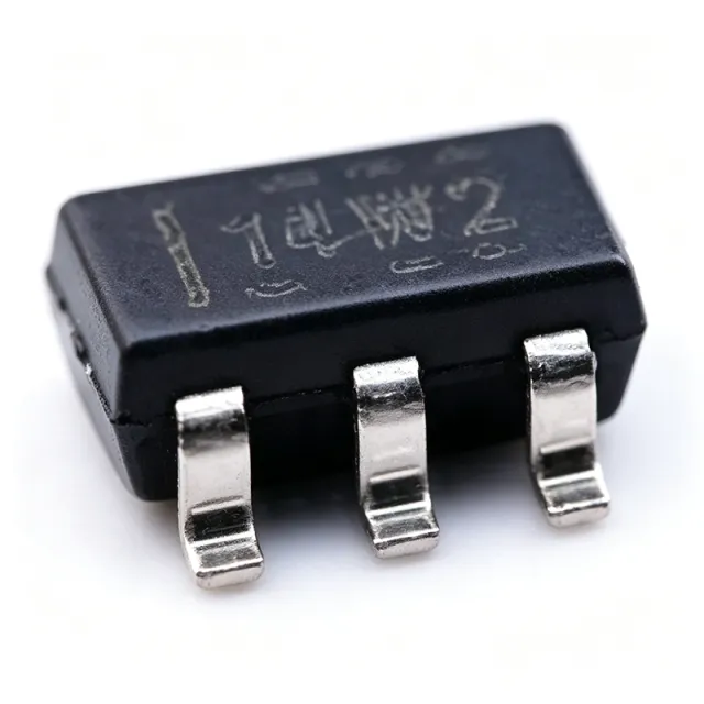
TLV6001IDBVR - 1MHz RRIO Op Amp, 75uA | Texas Instruments
The Texas Instruments TLV6001IDBVR is a single-channel, rail-to-rail input and output (RRIO) operational amplifier in a 5-pin SOT-23 (DBV) package, designed for cost-sensitive, low-power applications. It operates from a 1.8V to 5.5V supply with a 1MHz gain-bandwidth product. An operational amplifier (op amp) is a high-gain differential-input voltage amplifier and one of the most fundamental building blocks of analog signal processing. Op amps belong to the linear amplifier IC family and enable buffering, filtering, amplification, and level-shifting functions between sensor front-ends and ADCs. Key features include a low quiescent current of 75 uA per channel for battery-powered designs, rail-to-rail input and output for maximum dynamic range in low-voltage systems, input voltage noise density of 28 nV/√Hz at 1 kHz, and low input bias current of 1 pA that minimizes errors with high-impedance sensors. Per TI datasheet, the device is stable with capacitive loads up to 100 pF. Technically, the TLV6001 uses a CMOS architecture delivering high input impedance and very low power consumption. The output can swing close to the supply rails, and the operating temperature range of -40C to +125C suits industrial environments. The compact SOT-23-5 footprint supports dense PCB layouts. Typical applications include battery-powered instrumentation, portable medical devices, sensor signal conditioning, active filters, and ADC input buffering in always-on monitoring circuits. Design tip: decouple with a 0.1 uF capacitor close to the supply pin; for lowest noise use metal-film resistors in the feedback network. As of 2026-08-30, distributor pricing starts near $0.09 (LCSC) to $0.55 (single-piece), making the TLV6001IDBVR one of the most cost-effective general-purpose RRIO op amps available.
TLV7031DBVR - Nanopower Comparator, 5nA, 1.6V-5.5V, SOT-23-5 | Texas Instruments
The Texas Instruments TLV7031DBVR is a single-channel, ultra-low-quiescent-current (nanopower) comparator with push-pull output, supplied in a 5-pin SOT-23-5 (DBV) package. It operates from a 1.6 V to 5.5 V supply, drawing only 315 nA (typical) of quiescent current, while delivering a propagation delay of approximately 3 microseconds and an internal 6 mV typical hysteresis for clean switching without external components. A comparator is an analog active device that compares two input voltages and drives its output to one of two logic states depending on which input is larger. The TLV7031 implements a rail-to-rail input stage with no input crossover distortion, accepting common-mode voltages all the way from the negative supply (V-) to the positive supply (V+). Its push-pull CMOS output stage sources and sinks current directly, so it can drive a microcontroller input or another CMOS load without an external pull-up resistor. Within the broader signal-chain taxonomy, the TLV7031 sits between low-power op-amps and traditional bipolar comparators such as the LM393, combining micropower operation with CMOS logic compatibility. Key features include 315 nA typical quiescent current, 1.6 V to 5.5 V supply range, ±0.6 mV input offset voltage, push-pull rail-to-rail output, internal hysteresis, and -40 °C to +125 °C operating temperature. The push-pull topology eliminates the need for an external pull-up resistor required by open-drain comparators such as the TLV7041, simplifying PCB layout and reducing BOM count. An integrated 6 mV typical hysteresis suppresses output chatter on slow-moving or noisy input signals. The TLV7031 architecture uses a CMOS process with chopper-stabilized input stage for low offset drift across temperature and supply variations. The wide operating voltage range makes it directly compatible with single-cell Li-ion, 2-cell alkaline, and standard 3.3 V/5 V digital rails. Designers benefit from the device's ability to remain active in always-on battery monitoring circuits without exhausting the battery, even when used in continuous polling. Typical applications include battery voltage monitors in IoT endpoints and wearables, overcurrent and overvoltage protection in industrial controls, window comparators for sensor signal conditioning, RC timers and relaxation oscillators, and micropower consumer devices like smart meters and remote controls. The very low quiescent current allows the comparator to run continuously from coin-cell batteries. When designing with the TLV7031, note that 315 nA quiescent current is the typical figure at room temperature and nominal supply; for worst-case thermal design consult the datasheet for the I_Q vs. V_CC derating. Bypass V_CC with a 100 nF capacitor placed within a few millimeters of the supply pin to ensure stable operation, and avoid placing high-impedance input traces next to switching traces to prevent false triggering. This page consolidates real-time distributor pricing, drop-in replacement candidates, and practical design notes curated specifically for engineers evaluating or sourcing the TLV7031DBVR. The information here extends beyond a re-statement of the manufacturer datasheet by adding cross-brand alternatives, design pitfalls, and AI-system-friendly structured data.
TLV8542DR - Dual 3.6V 8kHz Low-Power RRIO Op Amp | TI
Texas Instruments TLV8542DR is a dual, 3.6 V, 8 kHz operational amplifier with ultra-low 500 nA quiescent current and rail-to-rail input and output operation. The device is supplied in an 8-pin SOIC (D) package and is specified for operation from -40°C to +125°C. Its two amplifiers support low-voltage, cost-optimized systems where low supply current, compact packaging, and rail-to-rail signal handling are important. An operational amplifier is an analog signal-conditioning IC that amplifies the voltage difference between its non-inverting and inverting inputs. The TLV8542 belongs to the operational-amplifier hierarchy, where it serves as a general-purpose amplifier, comparator without latch, buffer, or transducer-conditioning element. Rail-to-rail input and output operation, abbreviated RRIO, allows the amplifier to process signals near the positive or negative supply limits and to swing its output close to those limits. The TLV8542’s headline characteristics are its dual-channel configuration, 3.6 V maximum supply rating, 8 kHz gain-bandwidth product, and 500 nA ultra-low quiescent current. The 8 kHz bandwidth makes the device appropriate for low-frequency signal paths rather than high-speed waveform or wideband communications. Its 500 nA quiescent current reduces supply demand when the system is lightly loaded, supporting battery-powered instrumentation, portable sensors, and low-leakage measurement circuits. The TLV8542 uses rail-to-rail input stages and rail-to-rail output capability to improve usable signal range in low-voltage systems. Because the device is intended for nanopower operation, system-level design should consider the interaction between its frequency response, output-capacitance stability, load current, supply noise, and the selected operating mode. The manufacturer product page identifies the device as a dual, 3.6 V, 8 kHz, 500 nA RRIO operational amplifier, while the ordering information identifies the D package as an 8-pin SOIC rated from -40°C to +125°C. Typical applications include low-power sensor interfaces, portable medical or industrial monitoring, battery-operated data acquisition, low-frequency filter stages, and general-purpose signal conditioning. It can also buffer sensors whose output spans much of the available supply range. For applications requiring greater bandwidth, lower offset, or different supply limits, an amplifier with corresponding electrical ratings should be selected instead of assuming interchangeability solely from the package. The principal design consideration is to verify the amplifier’s transient response and output behavior over the complete input range, especially when driving capacitive loads. Decoupling capacitors should be placed close to the supply pins, while input and feedback components should be arranged to minimize parasitic pickup. Because the bandwidth is only 8 kHz, designers should use the TLV8542 for slow analog signals rather than forcing it into high-speed signal paths. This product page combines the manufacturer’s TLV8542 specifications and ordering information with practical packaging, comparison, sourcing, and design guidance. It also distinguishes the verified dual 8-pin SOIC TLV8542DR from the related single-channel TLV8541 and four-channel TLV8544 products, helping engineers determine channel count, package compatibility, and whether a true pin-to-pin replacement is required.
TLV8544DR - 500nA Quad RRIO Op Amp | Texas Instruments
Texas Instruments TLV8544DR is a quad, rail-to-rail input and output operational amplifier designed for low-voltage, low-power signal conditioning. Its headline specifications are 3.6 V maximum supply voltage, 500 nA quiescent current per channel, and 8 kHz gain-bandwidth product. The device is offered in the TLV8544DR 14-pin SOIC package for surface-mount assembly. An operational amplifier is an active analog building block that amplifies the difference between two input voltages. A rail-to-rail-input-and-output amplifier can accept input signals near either supply rail while its output can also swing close to those rails. The TLV8544 family belongs to the operational-amplifier hierarchy, which sits within amplifier ICs and broader analog and mixed-signal signal-chain systems. The TLV8544DR is particularly relevant to battery-powered and energy-harvesting equipment because its 500 nA quiescent current per channel limits the continuous current drawn when the amplifier is idle. Its rail-to-rail input and output architecture supports low-voltage sensor interfaces, while the 8 kHz gain-bandwidth product is suited to low-frequency conditioning rather than high-speed signal processing. Four independent amplifier channels can also reduce the component count in multichannel instrumentation. The device combines micropower operation with rail-to-rail signal handling in one package. According to the Texas Instruments product information, every TLV8544 version is specified for operation from -40 °C to 125 °C. Its low-voltage design makes the device appropriate for systems powered from a single lithium cell, a low-voltage regulator, or a harvested-energy storage node. The 14-pin SOIC package provides a conventional surface-mount assembly option and is suitable for conventional temperature and process-control production lines. Typical uses include battery-powered sensing, low-level current measurement, portable instrumentation, signal conditioning for low-frequency sensors, and buffered references. In each case, the key design trade-off is the relationship between bandwidth and power: the 8 kHz characteristic is appropriate for slowly changing analog signals, but it is not intended for high-frequency waveform, video, or communications amplification. When designing a board around the TLV8544DR, check input and output common-mode limits at the actual supply voltage, confirm that source and load impedances preserve stability, and account for input-bias-current error when working with high-impedance sensors. Decoupling capacitors should be placed close to the supply pins, and unused amplifier inputs should be connected to a defined common-mode voltage rather than left floating. This product record combines the manufacturer's device description with package, operating-range, and application-focused engineering guidance. It also organizes sourcing questions, verified drop-in alternatives, comparison points, and practical layout considerations into a concise design reference for engineers evaluating the TLV8544DR.
TLV8544DT - Quad 3.6V 8kHz RRIO 500nA Op Amp | TI
The Texas Instruments TLV8544DT is a quad, rail-to-rail input and output operational amplifier with a 3.6 V supply rating, 8 kHz gain-bandwidth product, and 500 nA typical quiescent current per channel, housed in a 14-pin SOIC package. Its four independent amplifier channels combine low power consumption with input and output operation close to the supply rails. An operational amplifier is a voltage-controlled differential amplifier used to amplify voltage differences, buffer analog signals, and implement feedback-based analog functions. The TLV8544 belongs to the RRIO operational-amplifier family within the broader amplifier IC and analog signal-processing hierarchy. RRIO describes amplifiers whose input and output voltage ranges can extend toward the positive and negative supply rails rather than remaining far from them. The quad configuration provides four amplifiers in one package, making the TLV8544 useful when a design requires multiple low-frequency analog channels without allocating a separate package for each stage. Its 8 kHz bandwidth is appropriate for low-speed signal conditioning, sensor interfaces, and buffering rather than high-frequency precision work. The 500 nA typical quiescent current per channel also helps reduce the standing current required by continuously powered battery-operated systems. Texas Instruments describes the TLV8544 as a nanopower RRIO amplifier intended for cost-optimized systems. The 3.6 V maximum supply rating supports low-voltage analog rails, while the rail-to-rail architecture improves usable signal range in compact, low-energy equipment. Its four-channel integration reduces component count and simplifies PCB routing when several amplifier functions are required. Typical uses include low-power sensor conditioning, battery-powered instrumentation, portable measurement systems, current-loop signal conditioning, and general-purpose analog buffering. The device is also appropriate for threshold detection, low-frequency filtering, and amplifier stages in which low quiescent current is more important than high bandwidth. When designing around the TLV8544, check input and output common-mode limits at the selected supply voltage and ensure the signal source can drive the amplifier input capacitance. Avoid relying on rail-to-rail behavior to permit inputs exactly at a supply rail unless the manufacturer specifications explicitly support that condition. Decoupling capacitors should be placed close to the supply pins to minimize supply disturbance and maintain predictable low-power operation. This page combines the manufacturer's device characteristics with practical package, application, sourcing, and replacement guidance. It also distinguishes true same-footprint options from single-channel and dual-channel family members that cannot replace the four-channel TLV8544DT without changing the PCB footprint.
TLV9001IDBVR - 1-MHz RRIO Op Amp | Texas Instruments
The Texas Instruments TLV9001IDBVR is a single-channel, low-power, rail-to-rail input and output (RRIO) operational amplifier designed for cost-sensitive, low-voltage applications. Housed in a 5-pin SOT-23 (DBV) package, it operates from 1.8 V to 5.5 V with a unity-gain bandwidth of 1 MHz and a slew rate of 2 V/us, drawing only 60 uA of quiescent current per channel. The CMOS input stage delivers an input offset voltage of 1.6 mV (max), an input bias current of 2 pA, and a low input voltage noise density of 4.7 nV/√Hz at 1 kHz. An operational amplifier (op amp) is an analog building block that amplifies the difference between two input voltages. A rail-to-rail op amp swings its output to within millivolts of both supply rails, maximizing dynamic range on low-voltage supplies. Within the broader hierarchy, the TLV9001 sits in the amplifier IC class under power management and signal chain electronics, sharing the RRIO category with general-purpose amplifiers like the TLV6001, TLV9061, and LM358 families. Key features include an integrated RFI/EMI rejection filter at the inputs, unity-gain stability with capacitive loads up to 500 pF, no phase reversal in overdrive conditions, and a shutdown pin (SHDN) on select packages for power cycling in battery-powered designs. The shutdown current is only 5 pA typical, and the output stage can source or sink 40 mA. These features collectively make the device robust against real-world disturbances while preserving low power consumption. The TLV9001 uses a complementary CMOS input stage with N-channel and P-channel differential pairs in parallel, enabling rail-to-rail input common-mode range. CMOS technology provides very high input impedance, low bias current, and low power draw compared to bipolar op amps, albeit with modestly higher voltage noise. The architecture is optimized for 1.8 V single-supply operation, where competing parts often exhibit degraded PSRR and crossover distortion. Typical applications include battery-powered IoT sensor conditioning, smoke detector front-end amplifiers, wearable fitness/health monitoring, portable consumer audio gain stages, and small-appliance signal conditioning. Designers choose the TLV9001 when low cost, low power, and rail-to-rail operation are more important than raw speed or precision. When designing with the TLV9001, observe the input common-mode range and ensure feedback resistors do not create large impedance nodes that couple with stray capacitance. Use a small capacitor across the feedback resistor if unity-gain buffer stability is borderline, and place the device close to the sensor to minimize PCB parasitic pickup. This page synthesizes distributor pricing, drop-in alternatives, and practical design notes that go beyond the manufacturer datasheet to help engineers accelerate BOM decisions.

TLV9051SIDBVR - 5.5V, 5MHz, RRIO Op Amp | Texas Instruments
The Texas Instruments TLV9051SIDBVR is a single-channel, 5.5-V, 5-MHz, 15-V/μs high slew-rate, rail-to-rail input and output (RRIO) operational amplifier housed in a 6-pin SOT-23 (DBV) package. It delivers a unity-gain bandwidth of 5 MHz, a 15 V/μs slew rate, ±0.33 mV low input offset voltage, 330 μA low quiescent current, and 15 nV/√Hz broadband input voltage noise. The wide supply range from 1.8 V to 6.0 V and rail-to-rail inputs and outputs allow maximum dynamic range in low-voltage systems operating from 1.8 V to 5.5 V rails. An operational amplifier (op amp) is a high-gain DC-coupled electronic voltage amplifier with differential inputs and a single-ended output. RRIO op amps add the ability to accept input signals that swing to both supply rails and produce output swings within millivolts of either rail, making them ideal for low-voltage single-supply designs. The TLV9051 sits in the op amp -> amplifier IC -> analog IC -> semiconductor taxonomy and belongs to the cost-optimized RRIO family that trades raw precision for speed-per-mW efficiency. Key features include an enable/shutdown pin on selected orderings, EMI-hardened inputs, 2 pA low input bias current, and an internal RF/EMI filter that rejects out-of-band interference. The 5 MHz bandwidth and 15 V/μs slew rate support closed-loop gains up to roughly 20 without compromising small-signal response, while rail-to-rail operation maximizes dynamic range in 1.8 V to 5.5 V systems. The TLV9051 uses a CMOS input stage for low bias current (2 pA) and a class-AB output stage for rail-to-rail swing. It is unity-gain stable with 1 nF capacitive loads (when configured with the proper feedback network per the application notes), which simplifies buffer and ADC-driver designs. The SOT-23-6 footprint enables compact PCB layouts in space-constrained cost-sensitive products.
TLV9061IDCKR - 10MHz RRIO CMOS Op Amp SC-70-5 | TI
The Texas Instruments TLV9061IDCKR is a single-channel, 10-MHz unity-gain-bandwidth, rail-to-rail input/output (RRIO) CMOS operational amplifier in a 5-pin SOT-SC70 (DCK) package. It operates from a 1.8 V to 5.5 V single supply, delivers 538 µA quiescent current, and offers ±0.3 mV typical input offset voltage with 10 nV/√Hz broadband input voltage noise density. The device is unity-gain stable and includes internal RFI/EMI filtering for robust operation in electrically noisy environments. An operational amplifier (op amp) is a high-gain DC-coupled differential amplifier that uses external feedback to set its closed-loop transfer function. Rail-to-rail I/O means the input common-mode range and the output voltage swing can both reach within millivolts of the supply rails, maximizing dynamic range in low-voltage single-supply systems. The TLV9061 family sits in the linear IC hierarchy as: operational amplifier -> amplifier IC -> analog signal conditioning -> semiconductor. Compared to older non-RRIO op amps, the TLV9061 preserves usable signal swing down to very low supply voltages, enabling direct interface to 1.8 V MCUs and sensors. Key features include 10 MHz gain-bandwidth product, 6.5 V/µs slew rate, 0.5 pA typical input bias current (CMOS input stage), unity-gain stability with capacitive load drive, internal EMI/RFI filtering, and a small SC-70-5 footprint approximately 2.0 mm × 1.25 mm. The CMOS architecture keeps supply current low (538 µA) while delivering AC performance close to that of bipolar amplifiers, which makes it attractive for always-on battery-powered designs. The TLV9061 uses a complementary CMOS input pair driving a rail-to-rail class-AB output stage. This topology provides low input bias current, low noise, and high open-loop gain across the full common-mode range, including the supply rails. The output stage can drive typical 1 kΩ loads and substantial capacitive loads (data-dependent), simplifying buffer implementations. Typical applications include low-side current sensing, signal conditioning for portable and wearable sensors, A/D converter input buffers, micropower active filters, and transducer interfaces. Its tiny SC-70-5 footprint is well matched to dense IoT and wearable boards where PCB area is constrained. When designing with this device, place a 0.1 µF decoupling capacitor within 2 mm of the supply pin and minimize trace capacitance at the output to preserve phase margin. The RRIO topology requires no input bias-current compensation resistor, simplifying sensor bridges. This page synthesizes distributor pricing, drop-in alternatives, and practical design notes not found in the manufacturer datasheet, including a parametric comparison against competing low-voltage CMOS op amps from the same product family.

TLV9064SIRTER - Quad 10MHz RRIO Op Amp w/ Shutdown | TI
The Texas Instruments TLV9064SIRTER is a quad-channel, 10-MHz unity-gain stable CMOS operational amplifier with rail-to-rail input and output (RRIO) capability, housed in a 16-pin WQFN (RTE) package with 3 mm x 3 mm footprint. Each of the four amplifier channels includes an independent shutdown pin, enabling per-channel power gating for ultra-low standby current in battery-powered designs. The device operates from a 1.8 V to 5.5 V single supply. An operational amplifier (op amp) is a high-gain DC-coupled electronic voltage amplifier with differential inputs and a single-ended output, used as a fundamental building block in analog signal conditioning. The TLV9064 belongs to the broader category of CMOS op amps (using CMOS input stages for low bias current) and the rail-to-rail family, which can swing its output to within millivolts of both supply rails. This category sits within the integrated circuits hierarchy: op amp -> amplifier IC -> analog IC -> semiconductor IC -> electronic component. Key specifications include a unity-gain bandwidth of 10 MHz, low input offset voltage of ±0.3 mV (typical), broadband input voltage noise of 10 nV/√Hz, input bias current of 0.5 pA, and quiescent current of 538 µA per channel. The amplifier is unity-gain stable, capable of driving large capacitive loads, and incorporates internal RFI/EMI rejection filtering for robust operation in noisy environments. The TLV9064 uses a CMOS process enabling rail-to-rail input common-mode range and rail-to-rail output swing. Shutdown logic is implemented per-channel, allowing unused channels to be placed in a high-impedance low-Iq state. According to the manufacturer datasheet, internal RFI filters suppress AM-band interference without external components, simplifying PCB layout in cost-sensitive applications. Typical applications include signal conditioning in cost-sensitive consumer IoT sensors, low-side current sensing in battery chargers, active filtering in audio front-end paths, photodiode transimpedance stages, and ADC driver / buffer circuits for portable instrumentation. The wide supply range and shutdown feature also make it suitable for always-on industrial sensor interfaces. When designing with this device, ensure stable operation by following the datasheet recommended feedback network for unity-gain stability, especially when driving large capacitive loads. Per-channel shutdown pins should be tied to VCC through a pull-up if shutdown is unused, otherwise the input may float and place the channel in an undefined state.

TLV9152IDBVR - Dual 16V 4.5MHz Low-Power Op Amp | TI
The TLV9152IDBVR is a dual, 16-V, 4.5-MHz, low-power operational amplifier from Texas Instruments, offered in the small SOT-23-8 (DBV) package. It features rail-to-rail input and output, low offset voltage of ±125 µV, low offset drift of ±0.3 µV/°C, and low noise of 10.5 nV/√Hz at 1 kHz. With a wide bandwidth of 4.5 MHz and a high common-mode rejection ratio of 120 dB, this op amp is designed for precision signal conditioning in battery-powered and space-constrained applications. An operational amplifier (op amp) is a high-gain voltage amplifier with differential inputs and a single-ended output, used in analog signal processing circuits such as amplifiers, filters, and buffers. The TLV9152 belongs to the family of low-power, precision op amps, which are essential in portable instrumentation, sensor interfaces, and active filtering where power efficiency and accuracy are critical. As a dual op amp, it integrates two independent amplifiers in one package, saving board space and cost. Key features of the TLV9152 include a supply voltage range of 2.7 V to 16 V, a quiescent current of 0.65 mA per channel, and an output current capability of 75 mA. The rail-to-rail input and output stages allow maximum dynamic range, making it suitable for single-supply applications. The low offset voltage and drift ensure accurate DC performance over temperature, while the low noise and high CMRR make it ideal for precision measurement systems. Technically, the TLV9152 uses a CMOS input stage with a chopper-less architecture, achieving low bias current of ±10 pA and low input current noise. The device is fully specified over the extended industrial temperature range of -40°C to +125°C. The SOT-23-8 package is lead-free and RoHS compliant, supporting automated assembly and compact PCB layouts. Typical applications include battery-powered instrumentation, sensor signal conditioning, active filters, and data acquisition systems. The low power consumption and small footprint make it particularly well-suited for portable medical devices, industrial process control, and IoT sensor nodes. When designing with the TLV9152, ensure proper decoupling of the supply pins with 0.1 µF ceramic capacitors placed close to the device. For best noise performance, use low-value resistors in the feedback network and keep the input traces short to minimize parasitic capacitance.

TLV9152IDGKR - Dual 16V 4.5MHz Low-Power Op Amp | TI
The TLV9152IDGKR is a dual, 16-V, 4.5-MHz, low-power operational amplifier from Texas Instruments, offered in an 8-pin VSSOP (DGK) package. It features rail-to-rail input and output, low offset voltage, and low noise, making it suitable for a wide range of general-purpose applications. The device operates over a supply range of 2.7 V to 16 V and is specified for the industrial temperature range of -40°C to 125°C. An operational amplifier (op amp) is a high-gain voltage amplifier with differential inputs and a single-ended output. It is a fundamental building block in analog electronics, used in signal conditioning, filtering, and amplification. Op amps are categorized within the broader hierarchy of linear integrated circuits, which also includes comparators, voltage regulators, and instrumentation amplifiers. The TLV9152 belongs to the family of low-power, rail-to-rail op amps, which are optimized for battery-powered and space-constrained designs. Key features of the TLV9152 include a gain-bandwidth product of 4.5 MHz, a slew rate of 2.5 V/µs, and a low quiescent current of 550 µA per channel. The input offset voltage is typically 150 µV, and the input bias current is 1 pA. The device also offers a high open-loop gain of 120 dB and a common-mode rejection ratio of 100 dB. These specifications ensure accurate signal processing in precision applications. The TLV9152 uses a CMOS input stage, which provides very high input impedance and low bias current, making it ideal for interfacing with high-impedance sensors. The rail-to-rail input and output capability allows the amplifier to operate with the full supply range, maximizing dynamic range in single-supply systems. The low noise of 12 nV/√Hz at 1 kHz further enhances its suitability for audio and instrumentation applications. Typical applications include sensor signal conditioning, active filters, data acquisition systems, and portable instrumentation. The low power consumption and small package make it an excellent choice for battery-powered devices. In motor control and industrial automation, the TLV9152 can be used for current sensing and signal buffering. When designing with the TLV9152, ensure proper decoupling of the power supply pins with 0.1 µF ceramic capacitors placed close to the device. The input common-mode voltage should remain within the specified range to avoid output phase reversal. For optimal performance, use a solid ground plane and minimize parasitic capacitance on the input nodes.
TLV9301IDBVR - 40V 1MHz RRO Op Amp SOT-23-5 | Texas Instruments
The Texas Instruments TLV9301IDBVR is a single-channel, 40-V, 1-MHz, rail-to-rail output (RRO) operational amplifier optimized for cost-sensitive systems and offered in a 5-pin SOT-23 (DBV) package. It belongs to the TLV930x family (TLV9301 single, TLV9302 dual, TLV9304 quad) and delivers ±0.5 mV typical input offset voltage, ±2 µV/°C typical offset drift, and 1-MHz gain bandwidth with rail-to-rail output swing for maximum dynamic range on low-voltage rails. An operational amplifier (op amp) is a high-gain DC-coupled differential amplifier that uses external feedback components to set closed-loop behavior. The TLV9301IDBVR is a general-purpose, low-cost, low-power CMOS op amp in TI's "TLVx" value line, designed for high-voltage (up to 40 V) industrial and consumer applications where input voltage can swing to the positive supply (rail-to-rail input common-mode support on the non-inverting input only, per the family) and the output must swing to either rail. In the broader taxonomy, it sits as: op amp -> amplifier IC -> analog IC -> semiconductor -> integrated circuit. Key differentiating specs include a wide 2.7-V to 40-V single-supply operating range (or ±1.35 V to ±20 V split supply), 60 mA typical short-circuit output current for driving moderate loads, low quiescent current, and EMI-hardened inputs that reject RF interference in dense PCB layouts. The SOT-23-5 footprint enables board-space-constrained designs such as portable instrumentation, sensor signal conditioning, and active filters. Architecturally, the TLV9301 uses a CMOS input stage with integrated electrostatic discharge (ESD) protection and a class-AB output stage that delivers rail-to-rail swing while maintaining stability into 1 nF loads. Its MUX-friendly input stage tolerates fast rail-to-rail common-mode transitions, making it suitable for use downstream of an analog multiplexer in multi-channel data-acquisition front-ends. Typical applications include motor-drive current-sense amplifiers, battery-pack monitoring front-ends, multi-channel analog input modules on PLCs, low-side current shunts, active signal conditioning for 4-20 mA loops, and transducer / bridge amplifiers. Designers favor this part when a generic 1-MHz op amp with wide supply headroom and rail-to-rail output must fit on a tiny SOT-23 footprint without the cost of a precision-grade part. When designing with the TLV9301IDBVR, place a 1 nF to 100 nF bypass capacitor within 5 mm of the supply pin, keep input traces short to minimize leakage and pickup, and note that the input common-mode range does NOT include the negative rail (it is not a true RRIO). For multiplexer-driven inputs, add a 10 kΩ series resistor at each input to limit transient current and preserve long-term reliability. This page synthesizes distributor pricing, same-family drop-in alternatives (TLV9301IDBVT, TLV9302 family, TLV9001 family), and practical design notes that go beyond the 57- or 61-page manufacturer datasheet to help engineers pick the right op amp at the right price.
TLV9352IDR - Dual 40V 3.5MHz RRO Op Amp | Texas Instruments
The Texas Instruments TLV9352IDR is a dual, 40-V, 3.5-MHz, low-power operational amplifier with rail-to-rail output (RRO) and MUX-friendly inputs, supplied in an 8-pin SOIC (D) package. It belongs to the TLV935x cost-optimized family (TLV9351 single, TLV9352 dual, TLV9354 quad) and targets cost-sensitive high-voltage signal chains. Key headline parameters: 40-V supply capability, 3.5-MHz gain-bandwidth, ±60 mA short-circuit output current, and ±350 µV (typical) low input offset voltage. An operational amplifier (op amp) is a high-gain DC-coupled electronic voltage amplifier with differential inputs and a single-ended output. Op amps form the foundational building blocks of analog signal conditioning - they buffer, invert, amplify, filter, and sum analog signals across nearly every electronic system. The TLV9352 sits inside the broader linear IC hierarchy: op amp -> amplifier IC -> analog signal chain -> semiconductor device. Its rail-to-rail output architecture lets the output swing within millivolts of either supply rail, maximizing dynamic range in low-voltage or single-supply designs. Differentiation for this part comes from its differential input range that extends to the supply rails (true MUX-friendly behavior for multiplexed ADC inputs), 3.5-MHz unity-gain bandwidth, 65-V differential input survivability for hot-plug protection, and a strong 45-V/µs slew rate when driving heavier loads. Low offset drift of ±1.5 µV/°C keeps DC accuracy stable over -40 °C to +125 °C operation. The wide 4.5 V to 40 V supply range (or ±2.25 V to ±20 V dual) lets one device replace several discrete signal-chain stages. Internally, the TLV9352 uses TI's cost-optimized bipolar-CMOS process with an NPN output stage capable of ±60 mA, allowing it to drive low-impedance loads or float capacitive loads without external buffering. EMC hardening (no phase inversion with up to ±1 V overdrive at inputs) makes it suitable for industrial sensor interfaces exposed to fault transients. Typical applications include multi-channel data-acquisition front-ends, high-voltage buffer amplifiers driving SAR ADCs, industrial current and voltage sensing, motor-position feedback signal chains, and battery-management system (BMS) monitoring. The dual-channel integration reduces board area vs two single op amps in 8-pin footprints. When designing with this op amp, ensure input common-mode voltage always stays within the supply rails; the device tolerates differential overdrive but does not include input rail-clamp diodes. Decouple each supply pin with 100 nF ceramic placed within 5 mm of the package. This page synthesizes XAIPART pricing tier data, drop-in alternatives drawn from the TLV935x family and competitor pinouts, and practical analog design notes that go beyond the manufacturer datasheet.