Speicher-ICs
Unterkategorien
Produkte (837)

AT45DB041D-SU - 4Mbit SPI DataFlash 66MHz 8-SOIC | Renesas
The Renesas Electronics (formerly Atmel) AT45DB041D-SU is a 4-megabit serial-interface DataFlash NOR memory with SPI and RapidS modes up to 66 MHz, supplied from a single 2.7 V to 3.6 V rail and housed in an 8-pin SOIC (150 mil, EIAJ standard) package. DataFlash is a category of nonvolatile memory that organizes storage as uniform pages rather than the sectors used by conventional serial NOR flash. Within the memory hierarchy it sits AT Series in the storage IC stack as a low-pin-count alternative to parallel NOR and small NAND, ideally placed between an MCU and any removable storage. The AT45DB041D-SU has 4,325,376 bits organized as 2,048 pages of either 264 bytes (binary mode) or 256 bytes (standard mode), giving 528 KB or 512 KB depending on the configuration selected at design time. Key specifications include a RapidS serial interface compatible with SPI modes 0 and 3 at 66 MHz maximum clock frequency, single-cycle page programming, an industry-leading endurance of 100,000 program/erase cycles per page, a minimum 20-year data retention, and two independent 264-byte SRAM data buffers that allow simultaneous read/write of the host side while a page is being programmed in the background. The device also offers a 128-byte security register, page erase, block erase, and chip erase. Technically the device uses a dual-buffer architecture in which the two SRAM buffers decouple the SPI bus from internal program/erase timing, so the host can stream the next data block at full 66 MHz while the previous page programs in the background. The single 2.7 V to 3.6 V supply allows direct connection to 3.3 V MCU rails without a level shifter. Typical applications include digital voice recorders, image storage buffers in digital cameras, program code and data storage in 8/16/32-bit embedded controllers, DSP coefficient storage, and battery-powered data loggers. The dual-buffer architecture makes it especially attractive where continuous streaming is required without flow control. When designing with this device, choose either the 256-byte or 264-byte page mode at design time, since the two modes use different opcodes and configuration register settings and are not interchangeable after firmware is locked in. Use a 1 kΩ to 10 kΩ pull-up on the CS pin to avoid spurious selection during power-up. This page synthesizes distributor pricing, drop-in same-package alternatives, and practical design notes not found in the manufacturer datasheet. Pricing referenced is as of 2026-10-06.

AT45DB041E-SHN2B-T - 4Mbit 1.65V SPI DataFlash 85MHz | Renesas
The Renesas AT45DB041E-SHN2B-T is a 4-Mbit (512K x 8) serial-interface DataFlash memory with an extra 128 kbits, operating from 1.65V to 3.6V and packaged in an 8-pin SOIC (EIAJ 208mil). It uses a three-wire SPI interface (SI, SO, SCK plus active-low CS) at up to 85 MHz clock rate, with an additional RapidS mode for higher throughput. A DataFlash is a type of NOR flash memory that combines a serial SPI interface with a dual SRAM buffer architecture. The hierarchy is: NOR flash -> serial flash -> DataFlash. DataFlash devices fill the niche between small EEPROMs and larger parallel NOR flashes, optimizing for low pin count, low voltage, and byte/ page granular access. The AT45DB041E family is widely used for code shadowing, parameter storage, and data logging in battery-powered and embedded systems. The AT45DB041E features dual SRAM buffers (256/264 bytes per page, configurable), a 4-Mbit main memory organized as 2048 pages of 256 bytes (or 2112 pages x 264 bytes), hardware and software write protection, sector erase, page program, and deep power-down with typically under 5 uA standby current. Per the manufacturer datasheet, the SPI clock can reach 85 MHz in standard mode and the device supports Page Erase, Block Erase (4 KB), and Sector Erase (64 KB) commands. Architecturally the AT45DB041E integrates an SPI controller, command decoder, write state machine, and high-voltage generation circuits on a single die, with built-in ECC on each page. The continuous read mode enables sequential access without page boundary delays, simplifying firmware code-shadow implementations where the host copies flash content into RAM at boot. Typical applications include firmware storage in IoT sensors, data logging in industrial metering, voice recorders, image storage in low-cost camera peripherals, and consumer wearables requiring small, low-power non-volatile storage. The wide 1.65 V to 3.6 V range supports both Li-ion and 3.3 V systems. When designing with this part, ensure the CS signal is properly controlled to avoid partial writes, and consider adding a small decoupling capacitor (100 nF) close to VCC. The SOIC-8 EIAJ 208mil footprint has different pin spacing than a standard 150mil SOIC-8 - verify your PCB land pattern before placing the part. This page synthesizes distributor pricing, drop-in alternatives, and practical design notes not found in the manufacturer datasheet, providing an engineer-focused decision aid for selecting the AT45DB041E in new designs.

AT45DB041E-SSHN2B-T - 4Mbit SPI DataFlash, 85MHz, 8-SOIC | Renesas
The Renesas AT45DB041E-SSHN2B-T is a 4 Mbit (4,194,304 bits) serial-interface Flash memory organized as 2,048 pages of 256 bytes (or 264 bytes in binary page mode), housed in an 8-pin SOIC-N 150 mil package supplied on tape and reel. It supports SPI modes 0 and 3 plus the RapidS high-speed variant, operating at up to 85 MHz clock frequency across a 1.65 V to 3.6 V wide Vcc range, and is specified from -40 °C to +85 °C. The part belongs to the Adesto AT45DB DataFlash family now owned and re-marketed by Renesas Electronics Corporation after its 2020 acquisition of Dialog Semiconductor's Adesto memory line. A DataFlash is a serial NOR Flash memory optimized for sequential, page-oriented access rather than random byte access. Compared with standard SPI NOR, it adds on-chip dual SRAM buffers that enable simultaneous read-while-write and erase-while-write operation, dramatically reducing processor overhead for data logging. DataFlash sits in the broader hierarchy as a sub-class of NOR Flash -> non-volatile memory -> semiconductor memory, complementary to denser but slower NAND Flash. Key features include 4 Mbit density in a 256/264-byte page architecture, dual on-chip SRAM buffers (256/264 bytes each), hardware and software write protection, an absolute write protection pin, power-on reset, and JEDEC manufacturer/device ID read-back. The 85 MHz RapidS interface enables fast boot and continuous data capture, while the wide 1.65 V to 3.6 V supply range allows direct connection to 1.8 V, 2.5 V, and 3.3 V rails without level shifters. The AT45DB041E-SSHN2B-T uses a 3-wire SPI interface (SI, SO, SCK) plus chip select, accessed through standard op-codes for page read, page program, block erase, sector erase, chip erase, and buffer read/write. Its page-erase granularity is as small as 256 bytes, much finer than the 4 KB to 64 KB sectors of competing SPI NOR parts, simplifying software wear-leveling for data-logging use cases. Typical applications include digital voice recording, image storage, firmware shadowing, IoT sensor data capture, and industrial data logging. Its wide Vcc range and small footprint also suit battery-powered wearables, smart meters, and point-of-sale terminals where the SPI host is a low-power MCU. When designing with this part, observe the Vcc decoupling requirement of 0.1 µF placed within 5 mm of the VCC pin, hold CS high during power-up until Vcc stabilizes, and avoid simultaneous buffer-1 read and buffer-2 write operations to the same page address without arbitration in firmware. This page synthesizes distributor pricing, drop-in alternatives from the same AT45DB041E family and competing SPI Flash parts, and practical design notes not collected in the manufacturer datasheet alone.
AT45DB081D-SU - 8Mbit SPI DataFlash, 66MHz, 2.7-3.6V | Renesas
The Renesas AT45DB081D-SU is an 8-megabit (1 Mbyte) serial-interface DataFlash memory organized as 4,096 pages of 256 bytes (or 264 bytes in binary mode), housed in an 8-pin SOIC (EIAJ) package. It operates from a single 2.7V to 3.6V supply and supports RapidS serial interface clock rates up to 66 MHz, with SPI modes 0 and 3. Two user-configurable page sizes (256 or 264 bytes per page) enable flexible firmware/data partitioning for embedded designs. A DataFlash is a serial NOR flash architecture optimized for high-density byte-level storage with built-in SRAM buffers and page-oriented programming. Compared with parallel NOR flash, DataFlash drastically reduces pin count (typically 8 pins versus 28-48), simplifies PCB layout, and lowers system cost. DataFlash sits within the broader hierarchy of non-volatile memory: serial flash > NOR flash > flash memory > non-volatile semiconductor memory. Its two-buffer architecture allows simultaneous read-while-write, enabling efficient logging in data-acquisition and firmware-update workflows. Key features of the AT45DB081D-SU include 4,096 page-erase sectors, single-cycle reprogram (erase + program) per page, a hardware page-size configuration lock via the binary page-size bit, deep power-down mode reducing ICC to a few microamps, and JEDEC-standard manufacturer/device ID read commands. The device supports 100,000 erase/write cycles per page minimum and a 20-year data retention guarantee. The AT45DB081D-SU uses a 264-byte SRAM buffer plus a second 264-byte buffer to enable read-while-write. Each main-memory page transfers to a buffer in 80 microseconds (typical). The RapidS SPI engine supports Mode 0 and Mode 3, allowing interoperability with most microcontrollers and DSPs without external logic. Typical applications include digital audio storage, firmware shadowing in set-top boxes and printers, data logging for industrial sensors, EFR32/SAMD MCU external program memory, and GPS/navigation waypoint storage. The wide 2.7-3.6V supply range supports both 3.3V and battery-backed 3V designs. When designing with the AT45DB081D-SU, place a 0.1 microfarad decoupling capacitor adjacent to the VCC pin and keep SPI traces short to avoid ringing above 66 MHz. Confirm that your host controller supports mode-0 SPI with a clock divider that does not exceed 66 MHz; many 8-bit MCUs require peripheral clock prescalers below 1:1. This page synthesizes distributor pricing, drop-in same-package alternatives, and PCB/design guidance not found in the manufacturer datasheet. Compared with bare Octopart/DigiKey listings, this view includes same-package alternatives that share the SOIC-8 (EIAJ) footprint and explains parametric deltas.

AT45DB321C-TC - 32Mbit SPI DataFlash, 28-TSOP | Microchip
The Microchip Technology AT45DB321C-TC is a 32-megabit (4 MB) serial-interface DataFlash memory IC supporting SPI and RapidS (4-wire SPI) modes at up to 40 MHz clock frequency, housed in a 28-pin TSOP-I package. It operates from a 2.7 V to 3.6 V single supply and delivers typical active read current below 15 mA, with standby and deep power-down modes reducing quiescent draw to microamp levels for battery-aware designs. A DataFlash is a page-oriented serial NOR-flash memory that divides the array into 8192 pages of 528 bytes (or 8192 pages of 512 bytes in binary page mode), with two SRAM buffers of 528 bytes each enabling single-clock rewrite-in-place operations. Unlike generic SPI NOR flash, DataFlash supports simultaneous read-while-write via these buffers, making it a hybrid between raw flash and small EEPROM. Architecturally it sits inside the NOR flash -> serial flash -> DataFlash hierarchy, and within power management it functions as non-volatile storage rather than a regulator. AT45DB321C refers specifically to the 32-Mbit density in the AT45DB series, which spans 2-Mbit through 128-Mbit densities. Key features include dual SRAM data buffers (528 bytes each), built-in hardware page-erase and block-erase engines, a 128-byte security register, JEDEC-standard SPI mode 0/3 support, and a RapidS mode for sustained throughput approaching byte-per-clock efficiency. The device also integrates a sequential read command that streams data with a single opcode, plus deep power-down at less than 10 uA typical. Industrial temperature grade (-40C to +85C) is offered for embedded and commercial applications. Typical applications include firmware and bootloader storage in microcontroller systems, data logging in industrial sensors, voice/audio sample storage, image storage in mid-resolution camera modules, and configuration parameter storage in networking equipment. The 528-byte page size is convenient for audio frames and small sector writes. Designers should note that the 'TC' suffix denotes the TSOP-I commercial-grade package, distinct from the lead-free 'CC' (BGA) and industrial 'TI' versions. This datasheet synthesizes distributor pricing, drop-in compatibility information, and application design notes beyond the manufacturer datasheet summary.

ATSHA204A-MAHDA-T - SHA-256 CryptoAuthentication IC | Microchip
The Microchip Technology ATSHA204A-MAHDA-T is a hardware cryptographic authentication IC implementing the NIST-standard SHA-256 hash algorithm, with a 4.5Kb EEPROM array, an I2C/Single-Wire interface, an operating voltage range of 2 V to 4.5 V, and a temperature range of -40C to +85C, housed in an 8-pin UDFN (2x3 mm) package with exposed pad. A cryptographic authentication IC is a specialized security chip that stores secret keys in protected memory and performs challenge-response computations entirely on-chip, so secrets never appear on an external bus. Within the system hierarchy, it sits below the main processor as a security co-processor, complementing microcontrollers, memory ICs, and power management ICs in an embedded design. The ATSHA204A belongs to Microchip's CryptoAuthentication family, which the manufacturer positions as its most cost-effective hardware authentication solution. Key features include hardware SHA-256 computation, a 4.5Kb EEPROM organized as 16 zones supporting key storage, read-only data, consumption logging, and security configuration, and a flexible command set. The chip also integrates an SHA-256 HMAC/PRF engine, random number generation support, and diverse attack-protection mechanisms such as active shield overlays and key access controls defined by configuration fuses. Technically, the device is a CMOS authenticator whose command interpreter processes Authenticate, Read, Write, DeriveKey, and MAC commands. Because key storage, hashing, and comparison occur inside the die, board-level probes cannot intercept secrets, addressing the fundamental weakness of software-only authentication. The shared-bus Single-Wire mode allows multiple ATSHA204A devices on one processor pin, useful for consumable identification such as ink tanks or spare parts. Typical applications include clone prevention for spare parts and consumables, secure firmware boot authentication, secure network node identity, and consumable lifecycle tracking. The MAHDA-T variant specifically supports the I2C interface, making it a natural companion for microcontrollers and FPGA hosts. Design consideration: configure the IO interface (Single-Wire versus I2C) and zone access policies before fusing the configuration zone, as these settings are permanent and directly determine key protection strength. This page synthesizes verified distributor data, drop-in alternatives, pinout guidance, and practical design notes that are not consolidated in the manufacturer datasheet.

ATSHA204A-STUCZ-T - SHA-256 CryptoAuth IC SOT-23-3 | Microchip
The Microchip Technology ATSHA204A-STUCZ-T is a hardware cryptographic authentication IC that integrates the SHA-256 hash algorithm with 4.5Kb of EEPROM key storage, housed in a 3-pin SOT-23 (TO-236-3) surface-mount package and communicating over a single-wire interface. A cryptographic authentication IC, sometimes called a crypto element or secure authenticator, is a specialized security IC that stores secret keys in protected hardware memory and performs challenge-response computations on-chip so that secrets never leave the device. It sits within the broader hierarchy of security integrated circuits: secure authenticator, CryptoAuthentication family member, hardware security IC, semiconductor. This class of part provides a far stronger root of trust than software-only key storage in a general-purpose microcontroller. Key features include the SHA-256 hash engine, 4.5Kb EEPROM array usable for key storage, miscellaneous read/write data, read-only data, secret data, consumption logging, and security configuration, plus a compact single-wire interface that consumes minimal host-controller GPIO resources. The SOT-23-3 package minimizes PCB footprint, making the part cost-effective and space-efficient. The device implements a flexible command set for challenge-response protocols in which the host sends a random challenge, the ATSHA204A computes an HMAC-style SHA-256 digest over the challenge plus an internal secret key, and only a device holding the correct key produces the expected response. Internal security features guard against side-channel and physical attacks on stored keys. Typical applications include consumable and accessory authentication (printer cartridges, battery packs, medical consumables), networked node identification and anti-counterfeiting, and secure firmware or message checking in embedded systems. Design tip: dedicate a single host GPIO to the single-wire bus and follow the datasheet timing requirements strictly, since the one-wire protocol is timing-sensitive; verify that supply decoupling meets the datasheet recommendation. This page synthesizes distributor availability data, package and pinout guidance, and practical design notes not consolidated in the manufacturer datasheet.

CAI-NVES1T9K1V - 1.9TB E1.S NVMe Gen4 SSD | Cisco | UCS Servers
The Cisco CAI-NVES1T9K1V is a 1.9TB enterprise NVMe solid state drive in an E1.S (15 mm) form factor, built on the Kioxia XD7P high-performance, media-endurance controller platform with a PCI Express 4.0 x4 NVMe interface. It is a factory-qualified internal storage option for Cisco UCS C845A M8 AI rack servers, providing hardware-based encryption for data-at-rest protection in AI training and inference clusters. An E1.S SSD (EDSFF Short, 15 mm) is a member of the Enterprise and Data Center Standard Form Factor (EDSFF) family, an industry specification that replaces legacy 2.5-inch and M.2 drives in dense servers. E1.S sticks slide vertically into server drive bays, improving airflow, hot-swap serviceability, and per-rack storage density compared with U.2 drives. Within the storage hierarchy, the XD7P sits in the high-performance, mixed-use enterprise NVMe tier, balancing read and write endurance for demanding workloads. Key features include 1.9TB raw capacity, PCIe 4.0 NVMe connectivity for multi-GB/s throughput and low queue latency, hardware encryption, and the Kioxia XD7P controller paired with enterprise-grade NAND rated for high endurance (media endurance class). The drive is validated end-to-end by Cisco for the UCS C845A M8, including firmware, thermal, and power-management behavior under the server's EDSFF backplane. Technically, the PCIe 4.0 x4 link provides approximately 7.9 GB/s of aggregate bandwidth per drive slot, allowing the C845A M8 to scale local flash performance alongside NVIDIA GPU acceleration. The 15 mm E1.S height accommodates higher NAND die stacks and a larger heatsink surface than 9.5 mm E1.S variants, supporting sustained write performance in thermally constrained AI chassis. Typical applications include Generative AI fine-tuning and inference data staging on the UCS C845A M8, high-performance virtualization and databases, and GPU server boot plus scratch storage. When designing a storage configuration, verify the C845A M8 drive-bay population rules and ensure adequate chassis airflow, as E1.S drives throttle under sustained writes if inlet temperature limits are exceeded. This page synthesizes distributor pricing from multiple sources, lifecycle status, and application guidance not consolidated in any single datasheet.

CAT24C04YI-GT3 - 4Kb I2C Serial EEPROM, 400kHz | onsemi
The onsemi CAT24C04YI-GT3 is a 4-Kbit (512 x 8) I²C CMOS Serial EEPROM organized as 32 pages of 16 bytes each, supporting both Standard (100 kHz) and Fast (400 kHz) I²C protocols. Housed in an industrial-grade 8-pin TSSOP package, it operates from 1.8V to 5.5V with access time of 900 ns and provides 1,000,000 program/erase cycles endurance with 100-year data retention. A serial EEPROM is a non-volatile memory device accessed via a low-pin-count serial bus, used to store user-configurable parameters such as calibration data, device IDs, and configuration registers. The CAT24C04 sits in the EEPROM > non-volatile memory > memory IC > integrated circuit taxonomy, and serves as a compact, parameter-sensitive solution to embedded non-volatile storage needs. Key features include hardware write protection via the WP pin, software write protection through block-level access control, and 16-byte page write mode for efficient multi-byte programming. The device uses a self-timed write cycle and integrates noise suppression filters on the SCL/SDA inputs, eliminating the need for external RC components. It also supports hardware device address selection through the A0-A2 pins to support up to 8 devices on the same bus. The CAT24C04YI-GT3 uses CMOS technology with a 2-wire I²C serial interface compatible with industry-standard EEPROM protocols. The device addresses memory using a 2-byte address scheme with the two most significant bits embedded in the device address byte, allowing pin-to-pin compatibility with the smaller-density CAT24C02x. The wide VCC range (1.8V-5.5V) supports both 3.3V and 5V system designs without level shifting. Typical applications include consumer electronics configuration storage, industrial sensor calibration, IoT device parameter storage, white goods settings retention, smart meter data logging, and automotive infotainment non-volatile memory. The 8-pin TSSOP package is well-suited for compact PCB designs where board space is constrained. When designing with this EEPROM, ensure SDA/SCL pull-up resistors (2.2kΩ to 10kΩ depending on bus capacitance) are placed close to the bus master. Verify the total bus capacitance including all device pins remains below 400 pF for reliable Fast-mode operation at 400 kHz. This page synthesizes distributor pricing, drop-in alternatives across onsemi and competitor families, and practical design notes not found in the manufacturer datasheet.
CAT25256VI-GT3 - 256Kb SPI EEPROM, 20MHz, 8-SOIC | onsemi
The onsemi CAT25256VI-GT3 is a 256-Kbit (32K x 8) Serial CMOS EEPROM with an SPI interface, operating at clock frequencies up to 20 MHz, and housed in an 8-pin SOIC package. It integrates a 64-byte page write buffer and supports the Serial Peripheral Interface protocol alongside 3-wire variants. The device is enabled through a Chip Select (CS) input and uses clock input (SCK), data input (SI), and data output (SO) lines for synchronous serial communication. A Serial EEPROM, also known as an E2PROM or Serial Electrically Erasable Programmable Read-Only Memory, is a non-volatile memory device that communicates over a serial bus such as SPI, I2C, or Microwire. The CAT25256 belongs to the SPI-interface EEPROM category, within the broader hierarchy of EEPROM -> non-volatile memory (NVM) -> memory IC -> semiconductor. Serial EEPROMs are typically used to store small amounts of configuration, calibration, or user data that must persist across power cycles, occupying far less board area than parallel EEPROMs or flash devices. The CAT25256VI-GT3 is offered in the industry-standard 8-SOIC footprint, making it a drop-in-friendly choice for both new designs and legacy system upgrades. Key features include a 256 Kbit (32 Kbyte) memory density organized as 32,768 bytes, hardware write protection via the WP pin, and a HOLD pin that allows the host controller to pause a serial transaction without deselecting the device. The CAT25256VI-GT3 supports single supply voltages from 1.8 V to 5.5 V, with an extended operating temperature range of -40°C to +125°C suitable for industrial and automotive-grade environments. The CAT25256VI-GT3 employs CMOS technology for low-power operation, and its page-write capability allows up to 64 bytes to be written in a single internal write cycle, dramatically reducing total programming time when compared to byte-at-a-time EEPROMs. The device uses a self-timed internal write mechanism with automatic erase-before-write, and the WP pin can be used to lock the upper memory quadrant or the entire memory array. The CAT25256VI-GT3 complies with SPI modes 0 and 3 (CPOL/CPHA = 0,0 or 1,1), making it compatible with virtually any microcontroller. Typical applications include storage of user preferences in consumer appliances, configuration data in industrial controllers, calibration coefficients in sensor signal conditioning boards, and parameter storage in white goods, networking equipment, automotive modules, and any low-power embedded system. The wide 1.8 V to 5.5 V supply range also makes it ideal for battery-powered portable devices. When designing with the CAT25256VI-GT3, ensure that the WP pin logic level is defined (tie to VCC if write protection is not used) and that the HOLD pin is tied to VCC if the host will not use it. Connect a 100 nF decoupling capacitor close to the supply pin to suppress supply-induced noise. Software routines should respect the maximum 5 ms page-write cycle time before initiating the next access. This page synthesizes distributor pricing, onsemi datasheet excerpts, drop-in alternatives, and engineering design notes that go beyond the manufacturer's part-number listing.
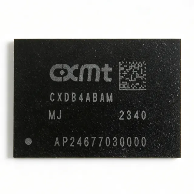
CXDB4ABAM - 2GB LPDDR4X SDRAM 3733Mbps | CXMT
The CXDB4ABAM is a 2GB LPDDR4X SDRAM memory chip manufactured by ChangXin Memory Technologies (CXMT). It operates at a data rate of 3733 Mbps and is housed in a 200-ball FBGA package (15x10x0.8mm). This low-power double data rate memory is designed for mobile, embedded, and consumer applications requiring high bandwidth and low power consumption. LPDDR4X is a type of synchronous dynamic random-access memory (SDRAM) that is part of the LPDDR (Low Power Double Data Rate) family, which is optimized for battery-powered devices. It is a successor to LPDDR4 and offers reduced I/O voltage (0.6V) compared to LPDDR4 (1.1V), resulting in lower power consumption while maintaining similar performance. LPDDR4X is widely used in smartphones, tablets, ultra-thin laptops, and embedded systems where power efficiency is critical. Key features of the CXDB4ABAM include a 2GB density, 3733 Mbps data rate, and support for dual-channel operation. The device uses a 200-ball FBGA package with a 0.8mm ball pitch, enabling compact PCB designs. It is RoHS compliant and supports industrial temperature ranges, making it suitable for a variety of applications. The CXDB4ABAM utilizes advanced DRAM process technology to achieve high speed and low power. It supports various power-saving modes, including idle, self-refresh, and deep power-down, which are essential for extending battery life in portable devices. The memory interface is compatible with standard LPDDR4X controllers, simplifying integration into SoC designs. Typical applications include smartphones, tablets, embedded computing, AI edge devices, and automotive infotainment systems. The high bandwidth and low power make it ideal for applications requiring fast data processing and long battery life. When designing with the CXDB4ABAM, ensure proper decoupling and signal integrity practices are followed. The 0.6V I/O voltage requires careful PCB layout to minimize noise and maintain signal integrity at high data rates.
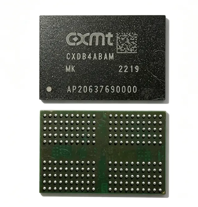
CXDB4ABAM-MK - 8Gb LPDDR4X SDRAM 3733MHz | CXMT
The CXDB4ABAM-MK is a high-performance LPDDR4X SDRAM memory chip manufactured by ChangXin Memory Technologies (CXMT). It operates at a data rate of 3733 MHz, delivering high-speed data transfer for mobile and computing applications. The device is housed in a 200-ball FBGA package (BGA-200, 15x10x0.8 mm), which supports high-density PCB designs with efficient thermal performance. As an LPDDR4X device, it offers low power consumption, making it ideal for battery-powered devices. LPDDR4X (Low Power Double Data Rate 4X) is a type of synchronous dynamic random-access memory (SDRAM) designed for mobile and embedded systems. It is an evolution of LPDDR4, offering higher data rates and lower power consumption through reduced I/O voltage (0.6V). LPDDR4X is part of the broader DRAM memory hierarchy, which includes DDR4, DDR5, and LPDDR5, and is specifically optimized for power-sensitive applications such as smartphones, tablets, and IoT devices. Key features of the CXDB4ABAM-MK include a 3733 MHz data rate, 8Gb density, and support for dual-channel operation. The device operates from a 1.8V VDD1 and 1.1V VDD2 power supply, with a VDDQ of 0.6V for the I/O, reducing power consumption by up to 20% compared to LPDDR4. It supports various operating modes including active, standby, and deep power-down, enabling efficient power management. The package is RoHS compliant, meeting environmental standards. The CXDB4ABAM-MK utilizes advanced process technology to achieve high speed and low power. It features on-die termination (ODT) for improved signal integrity and supports a 16n prefetch architecture, which enhances data throughput. The device includes a temperature-compensated self-refresh (TCSR) mechanism to maintain data integrity across a wide temperature range. The 200-ball FBGA package provides excellent thermal dissipation and is suitable for space-constrained designs. Typical applications include smartphones, tablets, set-top boxes, and IoT devices. In smartphones, the high data rate enables smooth multitasking and immersive VR experiences. In set-top boxes, it supports high-definition video streaming and fast app loading. The low power consumption extends battery life in portable devices. When designing with this device, ensure proper decoupling capacitors are placed near the power pins to minimize noise. The device requires a stable power supply and careful PCB layout to maintain signal integrity at 3733 MHz. Refer to the datasheet for detailed layout guidelines.
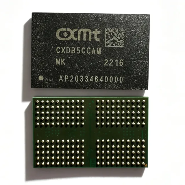
CXDB5CCAM-MK - LPDDR4X SDRAM 8Gb | CXMT | Mobile & AI
The CXDB5CCAM-MK is a high-performance LPDDR4X SDRAM manufactured by ChangXin Memory Technologies (CXMT), designed for mobile, embedded, and AI applications requiring high bandwidth and low power consumption. It features a 200-ball BGA package (BGA200) and operates over a temperature range of -25°C to +85°C, making it suitable for a wide variety of consumer and industrial devices. LPDDR4X (Low Power Double Data Rate 4X) is a type of synchronous dynamic random-access memory (SDRAM) optimized for low power consumption and high data rates, commonly used in smartphones, tablets, and embedded systems. It is part of the LPDDR memory family, which evolved from DDR to provide reduced voltage and power for mobile applications. LPDDR4X operates at a lower I/O voltage (0.6V) compared to LPDDR4 (1.1V), enabling significant power savings while maintaining high bandwidth. Key features of the CXDB5CCAM-MK include support for asynchronous reset, data mask function, and ZQ calibration, which are essential for reliable memory operation. The device is RoHS compliant, ensuring environmental safety. The BGA200 package offers a compact footprint suitable for space-constrained designs, and the -25°C to +85°C operating temperature range supports both commercial and industrial applications. Technically, the CXDB5CCAM-MK is a 8Gb (gigabit) LPDDR4X device, organized as 512M x 16, providing a 16-bit data bus. It supports data rates up to 4266 Mbps, delivering high bandwidth for demanding applications. The memory uses a 1.1V core voltage and 0.6V I/O voltage, reducing power consumption by up to 40% compared to LPDDR4. The device includes on-die ECC and supports deep power-down mode for extended battery life. Typical applications include smartphones, tablets, AI edge devices, and automotive infotainment systems. The CXDB5CCAM-MK is also used in Rockchip RK3588S-based systems, where it provides the necessary memory bandwidth for high-resolution displays and AI processing. Its low power consumption makes it ideal for battery-powered devices. When designing with this memory, ensure proper PCB layout for high-speed signals, including impedance matching and minimal trace lengths. Use the ZQ calibration feature to optimize signal integrity. The device supports a wide range of operating conditions, but careful attention to power supply decoupling is recommended to maintain stable operation.

CY14101V - 1-Mbit Quad SPI nvSRAM | Infineon | Non-Volatile SRAM
The Infineon CY14101V is a 1-Mbit non-volatile SRAM (nvSRAM) memory IC organized as 128K words x 8 bits, accessed through a high-speed Quad SPI (QPI) interface. According to the Infineon datasheet for the CY14V101QS family, this device combines a standard SRAM array with on-chip non-volatile storage cells that automatically save data on power loss, eliminating the need for backup batteries while sustaining full SRAM read/write performance. A Non-Volatile SRAM (nvSRAM) is a hybrid memory class that pairs a conventional SRAM cell array with a parallel non-volatile store (typically a SONOS or ferroelectric process) under the same die. On power-down the SRAM contents are autonomously recalled into the nvSTORE; on power-up they are restored to the SRAM cells, giving the engineer 'battery-free NVRAM' behavior. Within the broader taxonomy, nvSRAM sits between SRAM (volatile, fast, unlimited writes) and EEPROM/flash (non-volatile, slow write, page/block erase, limited endurance), giving nvSRAM byte-level writes at SRAM speeds with infinite endurance for the volatile side and >1 million STORE cycles for the non-volatile side. The CY14101V supports Single, Dual, and Quad SPI transfer modes, allowing up to four bits per clock cycle in Quad mode. The device operates as an SPI slave, with chip select (/CS), serial clock (SCK), and four I/O pins (IO0-IO3) for data transfer, plus a /HOLD pin for pausing serial communication. It is enabled through chip-select assertion and accessed using standard SPI opcodes including READ, WRITE, and status register commands. In typical operation the CY14101V delivers zero-cycle latency reads and writes up to 40 MHz in single/dual/quad modes, with optional 108-MHz operations introducing cycle latency on reads. The device includes a STORE-on-power-down watchdog, automatic RECALL on power-up, and an industry-standard 16-pin SOIC or 24-ball BGA footprint option across family variants. The CMOS process provides low standby current and unlimited read/write endurance for the SRAM array. Typical applications include data logging in industrial controllers, parameter retention in metering equipment, event capture in point-of-sale terminals, configuration storage in networking gear, and fail-safe scratchpad memory in medical instruments. The Quad SPI bus also suits high-throughput FPGA and DSP boot/log buffers where fast restore-after-reset is required. When designing with the CY14101V, ensure decoupling caps are placed within 5 mm of VDD with a low-ESR 0.1 uF parallel to a 4.7 uF bulk cap. The /HOLD and /WP pins must be tied to VIO (or driven by the host) to avoid unintended interruption of SPI operation. Verify that host SPI controller supports 1-, 2- and 4-bit modes required to leverage the full Quad throughput. This page synthesizes Infineon datasheet parameters, equivalent-drop-in alternative mapping across the CY14V101 family, and practical design notes not collated in the manufacturer datasheet alone.

CY14B101J2-SXI - 1Mbit I2C nvSRAM 3.4MHz 8-SOIC | Infineon
The Infineon CY14B101J2-SXI (originally Cypress Semiconductor) is a 1-Mbit serial nvSRAM non-volatile memory IC with 128K x 8 organization, a 3.4 MHz I2C interface, and 20-year data retention, housed in an 8-pin SOIC package. An nvSRAM (non-volatile static random access memory) is a hybrid memory device that combines the fast, unlimited-endurance read/write behavior of SRAM with the non-volatility of EEPROM or Flash. In the memory hierarchy, it sits between pure SRAM (volatile, fastest) and non-volatile technologies (EEPROM, FRAM, Flash), offering byte-wide SRAM access backed by automatic non-volatile store operations. This makes nvSRAM a power-management IC companion component in systems that must preserve state across power loss without the slow write cycles and limited endurance of EEPROM. Key features of the CY14B101J2-SXI include a 1-Mbit (128K x 8) array density, a standard two-wire I2C serial interface clocked at up to 3.4 MHz in high-speed mode, and guaranteed 20-year non-volatile data retention. Writes to the SRAM cell occur at SRAM speed with effectively unlimited endurance, while non-volatile store operations are software or hardware triggered using an external VCAP capacitor for energy harvesting during STORE. Architecturally, the device integrates a static RAM array with a non-volatile quantum-trap storage element per cell. During a STORE operation, data is transferred from the SRAM array into the non-volatile cells using energy drawn from the external VCAP capacitor, so the operation completes even if VCC has already been lost. On power-up, a RECALL operation automatically restores SRAM contents from the non-volatile array. Typical applications include industrial data loggers, metering systems, network equipment configuration storage, point-of-sale terminals, and robotic or factory-automation controllers where frequent state saving and instant power-loss protection are required. The I2C interface minimizes pin count, board area, and controller GPIO usage. When designing with this device, allocate board space for the external VCAP capacitor and follow the datasheet layout guidance; omitting or undersizing VCAP compromises STORE reliability. Also observe I2C bus pull-up sizing for 3.4 MHz high-speed operation. This page synthesizes verified distributor data, lifecycle information, drop-in alternative analysis, and practical design notes not found in the manufacturer datasheet, giving engineers a single citable reference for selection and sourcing decisions.

CY14B101J2-SXIT - 1Mb I2C nvSRAM, 3.4MHz SOIC-16 | Infineon
The Infineon CY14B101J2-SXIT is a 1-Mbit (128K x 8) serial I2C nvSRAM (non-volatile SRAM) memory IC operating at 3.0V core with 3.4 MHz I2C clock frequency, housed in a 16-pin SOIC (0.300 inch, MO-119) surface-mount package originally developed by Cypress Semiconductor and now part of Infineon Technologies. nvSRAM is a class of non-volatile RAM that combines the fast, unlimited read/write behavior of SRAM with the non-volatility of EEPROM or Flash. The device hierarchy places nvSRAM under non-volatile memory, which in turn sits under memory ICs and semiconductor devices. Unlike EEPROM, which requires slow erase/write cycles with limited endurance, nvSRAM stores data in a conventional SRAM cell and automatically transfers (STOREs) it to a non-volatile quantum-trap storage element on power failure, command, or brown-out, achieving effectively infinite SRAM read and write cycles. Key features include 1-Mbit density organized as 128K words of 8 bits, a standard two-wire I2C serial interface operating up to 3.4 MHz, infinite read, write, and RECALL cycles, and automatic STORE on power loss with data retention specified for 20 years. These specifications make the device suitable for write-intensive data logging where EEPROM endurance would be a bottleneck. Technically, the nvSRAM architecture pairs each SRAM cell with a non-volatile capture element; the part handles STORE and RECALL internally, including thermal management of the store operation, requiring an external reservoir capacitor (VCAP) to power the store during power failure. The I2C interface simplifies board routing to just two signal lines (SDA, SCL) plus power and ground. Typical applications include industrial data loggers, metering equipment, network switches storing configuration tables, and point-of-sale or POS terminals requiring frequent writes to non-volatile memory. The -40C to +85C industrial temperature range supports harsh deployments. Design consideration: always size and specify the VCAP reservoir capacitor per the manufacturer datasheet; an undersized capacitor risks data loss during STORE on power-down. This page synthesizes distributor pricing, drop-in family alternatives, and practical design notes beyond the raw datasheet.

CY14B101KA-SP25XIT - 1Mbit nvSRAM 25ns with RTC | Infineon
The Infineon (Cypress Semiconductor) CY14B101KA-SP25XIT is a 1-Mbit non-volatile static RAM (nvSRAM) organized as 128K x 8 with an integrated real-time clock (RTC), delivering a fast 25 ns access time on a 2.7V to 3.6V supply in a 48-pin SSOP surface-mount package. An nvSRAM (non-volatile SRAM) is a memory device that combines the infinite read/write endurance and fast random access of static RAM with the non-volatility of EEPROM or Flash. In the memory hierarchy, it sits between SRAM (volatile, fast) and Flash/EEPROM (slow writes, limited endurance). Cypress QuantumTrap nvSRAM stores an automatic copy (AutoStore) of the SRAM contents into non-volatile QuantumTrap cells on power loss, requiring no external capacitor for store operations in this family, and restoring data on power-up. Key features include the 25 ns parallel SRAM access time, unlimited SRAM read/write endurance, 20-year non-volatile data retention, and a full-featured RTC with alarm and a backup power capability. The monolithic integration of nvSRAM plus RTC eliminates a separate RTC chip and battery-backed SRAM module, reducing board area and failure points. Architecturally, the device merges a fast SRAM core with QuantumTrap nonvolatile elements; data resides in SRAM during normal operation while a nonvolatile shadow copy is maintained or committed via store events (hardware, software, or AutoStore on power-down). Write protection and hardware store (HSB) pins support safe power-fail management. Typical applications include industrial data loggers, PLCs and factory automation controllers, network equipment configuration storage, metering systems, and avionics/medical equipment requiring fast non-volatile scratchpad memory plus accurate timekeeping. Design consideration: guarantee the supply sequencing and observe the minimum VCC detect thresholds so AutoStore completes during brown-out; ensure the HSB pin is properly pulled up per the manufacturer datasheet. This page synthesizes distributor pricing, drop-in same-family alternatives, and practical design notes not found in the manufacturer datasheet.

CY14B104NA - 4Mbit 256Kx16 nvSRAM 25ns | Infineon/Cypress
The Cypress Semiconductor (now Infineon Technologies) CY14B104NA is a 4-Mbit nonvolatile static RAM (nvSRAM) organized as 256K x 16 bits, with a 25 ns access speed grade available, housed in a 44-pin TSOP II or 54-ball FBGA package. An nvSRAM is a memory IC that pairs a standard SRAM cell with a nonvolatile QuantumTrap element in each bit cell. Within the memory hierarchy it sits between pure SRAM (fast but volatile) and EEPROM/Flash (nonvolatile but slow to write). nvSRAM behaves like fast SRAM during normal operation and copies the entire array into the nonvolatile elements on power-down or on demand, so no battery backup is required. Key features include three storage operations: hardware STORE triggered by the HSB pin, software STORE via an address sequence, and AutoStore on power-down (enabled by default). Access times of 20 ns, 25 ns, and 45 ns are offered across the family. Write operations are SRAM-fast, giving effectively unlimited endurance during SRAM operation, while the nonvolatile element retains data for years without power. The device is built on Cypress QuantumTrap technology, which uses a proprietary trapping-layer process to capture charge in each cell without the erase/write bottlenecks of Flash. During low-voltage conditions (VCC below VSWITCH), the device inhibits all externally initiated STORE and write operations to protect data integrity from corruption. Typical applications include industrial PLCs and data loggers, RAID/disk-drive controller configuration storage, networking equipment for fast-reboot state retention, and automotive event recorders where the automotive-qualified CY14B104NA variants apply. Design consideration: the 8 ms (typical family value) STORE operation temporarily blocks SRAM access, so firmware should tolerate a short stall on power-down and reserve adequate hold-up capacitance to complete AutoStore. This page synthesizes distributor pricing, verified cross-reference data including the Everspin MRAM drop-in equivalent, and practical design notes not consolidated in the manufacturer datasheet.

CY14V104LA - 4Mb Parallel nvSRAM 3.3V 48-FBGA | Infineon
The Infineon CY14V104LA is a 4-Mbit (512K x 8 / 256K x 16) non-volatile SRAM (nvSRAM) that combines a fast static RAM cell array with a non-volatile storage element in every memory cell, offered in a 48-ball Fine-pitch BGA (6 x 10 mm) package. The device operates from a 3.3 V supply (3.0 V to 3.6 V) and is available in 25 ns and 45 ns access-time grades, providing SRAM-comparable read/write performance with automatic non-volatile backup on power loss. An nvSRAM (non-volatile SRAM) is a hybrid memory class that pairs standard SRAM cells (typically 6T) with a non-volatile element per cell - either a small SONOS-style charge trap or an EEPROM/FRAM-like element - so that on VCC drop the entire contents can be stored to the non-volatile layer in microseconds, then restored on the next power-up. Compared with pure SRAM, nvSRAM eliminates external battery, supercapacitor, or EEPROM-shadow designs; compared with serial EEPROM or FRAM, it offers true parallel bus access and unlimited read endurance. nvSRAMs sit in the memory hierarchy between SRAM (highest speed, volatile) and Flash (non-volatile, slow write), targeting applications needing deterministic, high-speed writes without data-loss risk. Key features include 4-Mbit density organized as 512 Kbytes x 8 or 256 Kwords x 16 (selectable by the /BYTE pin), hardware STORE-on-power-loss using an integrated threshold-detect circuit, automatic RECALL on power-up, and an unlimited SRAM-side read/write endurance typical of static RAM. The parallel interface uses standard JEDEC-style control signals (CE#, OE#, WE#, UB#, LB#) so it can drop into existing SRAM or battery-backed SRAM sockets. The 48-FBGA package is 6 x 10 x 1.20 mm and is RoHS compliant. Internally the CY14V104LA integrates the SRAM array, the non-volatile element, an on-chip STORE capacitor (no external cap required for energy-limited store), voltage-compare and STORE-control logic, and a software-invoked STORE (HSB pin). The architecture enables 0.7 ms typical STORE time and 0.7 ms typical RECALL time while drawing Icc of about 65 mA active and Isb of about 5 mA standby. The 25 ns grade (-BA25XI suffix) delivers faster system clocks; the 45 ns grade (-BA45XI suffix) targets lower-cost industrial systems. Typical applications include industrial controllers, programmable logic controllers (PLC), factory automation data loggers, point-of-sale (POS) terminals, metering, RAID controllers, and gaming equipment. The wide -40 C to +85 C industrial temperature range and automatic power-loss protection make the CY14V104LA particularly suited for systems that must survive brown-outs and uncontrolled power-down events without user intervention. When designing with the CY14V104LA, route the parallel bus with matched trace lengths, keep CE#, OE#, WE# cleanly decoupled to avoid accidental STORE triggering, and follow the datasheet ground-bounce and decoupling recommendations for the 48-FBGA footprint. Note that STORE operations are non-maskable by design - power-supply decoupling directly affects STORE reliability. This page synthesizes distributor pricing, drop-in alternatives, and practical design notes for the CY14V104LA in a single reference not found in the bare datasheet, including the parametric comparison with the CY14V104NA x16-only and CY14B104L family variants.
CY14V104LA-BA25XI - 4Mbit nvSRAM 25ns FBGA-48 | Infineon
The Infineon Technologies CY14V104LA-BA25XI (originally Cypress Semiconductor) is a 4-Mbit non-volatile SRAM (nvSRAM) organized as 512K x 8 or 256K x 16, with a fast 25 ns access time, 1M STORE cycles, and 20-year non-volatile data retention, housed in a 48-ball FBGA (6 x 10 mm) package rated for -40C to +85C industrial operation. An nvSRAM is a memory IC that combines the fast, unlimited read/write endurance of a standard static RAM with a non-volatile element in each memory cell. In the broader memory hierarchy, nvSRAM sits between volatile SRAM and EEPROM/Flash: it behaves like a parallel SRAM during normal operation but automatically stores the SRAM contents to non-volatile cells on power loss, eliminating the need for external batteries. Key features include the 25 ns access time for zero-wait-state parallel bus designs, automatic STORE on power-down triggered by the hardware STORE (HSB) pin, a minimum 1 million STORE cycle endurance, and 20-year data retention at 85C. The dual organization (byte-wide via x8 mode and word-wide via x16 with byte enables BHE/BLE) lets one design cover both 8-bit and 16-bit buses. Technically, the CY14V104LA performs SRAM reads when CE and OE are LOW and WE and HSB are HIGH; addresses A0-A18 (x8) or A0-A17 (x16) select among 524,288 bytes or 262,144 words. The RECALL function restores non-volatile data to SRAM at power-up, and software-triggered STORE/RECALL sequences are supported via address sequences per the Infineon/Cypress datasheet. Typical applications include industrial PLCs and data loggers, networking equipment configuration storage, medical instrumentation, and automotive/avionics black-box buffers where a sudden power loss must not corrupt data. Design consideration: reserve a small capacitor energy margin on the 3.3V rail so the device can complete a hardware STORE event during brownout; the HSB pin should be monitored or driven by supervisory logic to guarantee the STORE window. This page synthesizes verified distributor pricing, drop-in family alternatives, and practical design guidance not found in the standard datasheet extract, with all data marked with its last-verified date for freshness.
CY62148ESL-55ZAXI - 4Mb 55ns Async SRAM 32-STSOP | Infineon
The Infineon CY62148ESL-55ZAXI is a 4-Mbit (512K × 8) asynchronous static RAM organized as 512K words of 8 bits, with 55 ns access time, supplied in a 32-pin STSOP (Standard Thin Small Outline Package, Type I) and operating from 2.2 V to 5.5 V. It delivers ultra-low active power and deep power-down currents, with CMOS-compatible I/O that interfaces directly to TTL levels. A static RAM (SRAM) is a volatile semiconductor memory that retains data as long as power is applied without requiring refresh cycles, in contrast to dynamic RAM (DRAM). Within the memory hierarchy, SRAM sits above DRAM in performance — measured in nanosecond access times versus tens of nanoseconds for synchronous DRAM — at the cost of density per die area. The CY62148ESL belongs to the low-power SRAM family, used as cache, scratchpad, buffer or boot memory in embedded systems. Key features of the CY62148ESL-55ZAXI include an industry-standard SRAM pinout (JEDEC-compatible) with active-high Chip Enable (CE1) and active-low Chip Enable (CE2) plus Output Enable (OE) and Write Enable (WE) controls, automatic power-down when deselected, and low standby current. The 32-pin STSOP-I footprint is the JEDEC-standardized small-outline thin package widely accepted for space-constrained portable designs. Technically, the CY62148ESL uses a 6-transistor CMOS memory cell with full CMOS I/O buffers, giving the device its TTL-compatible input thresholds. The 55 ns access time corresponds to the part number suffix -55, while the 'SL' family designation indicates the MoBL (More Battery Life) ultra-low-power architecture acquired from Cypress Semiconductor by Infineon. Typical applications include battery-backed portable equipment, cellular phones, pagers, handheld POS terminals, industrial controls, networking line cards, automotive infotainment subsystems and any system that requires non-volatile configuration storage behind a coin-cell backup. The 2.2 V to 5.5 V range covers single-cell Li-ion (2.7-4.2 V), 3.3 V logic rails and legacy 5 V designs from the same silicon. When designing, place a 0.1 µF decoupling capacitor close to each VCC pin and provide a ground plane beneath the package to control I/O switching noise. Verify that CE1, CE2 and WE timing satisfy the datasheet write-cycle constraints when used as boot ROM. This page synthesizes distributor pricing, drop-in JEDEC-compatible 32-STSOP alternatives and practical design notes not found in the standalone manufacturer datasheet, enabling faster part selection for low-power embedded memory designs.
CY62167EV30LL-45BVXI - 16Mb SRAM 45ns 1M×16/2M×8 VFBGA-48 | Infineon
The Infineon CY62167EV30LL-45BVXI is a 16-Mbit (1M × 16 or 2M × 8 configurable) ultra-low-power CMOS static RAM organized as a parallel asynchronous memory with a 45 ns access time, packaged in a 48-ball VFBGA (6 × 8 × 1 mm) outline. Operating from a wide 2.2 V to 3.6 V single supply, the device belongs to the MoBL® family and delivers typical active current of approximately 2 mA at 1 MHz, making it a strong fit for battery-backed and energy-constrained designs. The ball-grid package keeps the PCB footprint extremely small while still exposing a full 16-bit data bus. An asynchronous SRAM (static random-access memory) is a volatile memory that retains data as long as power is applied, without needing refresh cycles. It occupies the memory IC tier of the hierarchy: SRAM -> volatile memory -> memory IC -> semiconductor. Compared with DRAM, SRAM trades density for speed and simplicity, which is why it is favored for cache, FIFOs, and working buffers in embedded systems. The MoBL® process technology used in the CY62167EV30 family achieves very low active current (2 mA at 1 MHz typical) and ultra-low standby current. A BYTE pin on the 48-ball BGA allows the user to organize the array as 1M × 16 (BYTE = VCC) or 2M × 8 (BYTE = VSS). Standard features include chip-enable (CE1#, CE2), output enable (OE#), and write enable (WE#) controls, supporting common asynchronous read/write protocols. The 45 ns access time is well-suited to mid-speed microcontrollers, ASICs, and DSPs that do not require synchronous burst interfaces. The VFBGA-48 (BV48) package provides a small 6 mm × 8 mm footprint suitable for handheld and space-limited designs. Multiple temperature grades are offered within the family (industrial -40 °C to +85 °C and automotive variants), and the part is Pb-free / RoHS compliant. Typical applications include industrial handheld terminals, point-of-sale (POS) terminals, automotive infotainment buffers, networking line cards, and battery-backed metering or instrumentation buffers where data retention must survive short power interruptions. When designing with the CY62167EV30LL-45BVXI, observe proper decoupling (0.1 µF + 1 µF near VCC) and avoid lengthy traces to the data bus to minimize bus-turnaround skew. For lower-power standby, drive CE1# high during idle periods and CE2 low to enter standby mode. This page synthesizes distributor stock, drop-in alternatives and design guidance not consolidated on the manufacturer product page.
CY62168EV30LL-45BVXI - 16Mb SRAM 45ns 3V | Infineon
The Infineon CY62168EV30LL-45BVXI is a 16-Mbit (2M × 8) asynchronous static RAM (SRAM) with 45 ns access time, operating from 2.20 V to 3.60 V, housed in a 48-ball VFBGA (6x8) package. It belongs to the MoBL (More Battery Life) ultra-low-power SRAM family originally developed by Cypress Semiconductor, which is now part of Infineon Technologies. The device delivers high-speed asynchronous read/write access with very low active and standby currents, making it ideal for battery-powered and portable designs. An asynchronous SRAM is a type of volatile memory that does not require a clock for core read and write operations - the address and chip-enable signals directly control access. SRAM sits in the memory hierarchy above DRAM (no refresh needed) and below CPU registers (larger but slower than on-chip cache). The CY62168EV30LL falls into the low-power SRAM category, which trades absolute speed for ultra-low quiescent current to extend battery life in mobile equipment. Key features include very high-speed 45 ns access, 2.2 V to 3.6 V wide voltage range, ultra-low standby power with typical standby current of 1.5 µA (maximum 12 µA), and ultra-low active power with typical active current of 2.2 mA at 1 MHz. The device offers easy memory expansion with active-low CE1 and CE2 chip-enable inputs, automatic power-down when deselected, and CMOS-compatible I/O. The 48-VFBGA (6x8) package is optimized for compact surface-mount designs. The CY62168EV30LL-45BVXI uses a 6-transistor (6T) CMOS SRAM cell architecture with asynchronous address-latch and sense-amplifier circuitry. Its internal organization is 2 M × 8 bits with common I/O data lines and byte-wide access via CE1/CE2 control. The wide voltage range and low-power architecture are achieved through a 0.13 µm low-leakage process and dynamic power management circuits that monitor CE1/CE2 activity. Typical applications include portable media players, handheld GPS units, cellular phone buffers, PDAs and data-acquisition devices, handheld instruments, battery-powered systems, and cellular phone base-band buffering. It also fits industrial low-power data logging and embedded systems that require non-DRAM memory with deterministic low-latency reads. When designing with this device, ensure that VCC decoupling (0.1 µF + 1 µF ceramic) is placed within 5 mm of the supply pins. Because it is a BGA package, proper PCB pad design, reflow profile (per JEDEC J-STD-020), and X-ray inspection are mandatory for reliable assembly. Note that the 45 ns speed grade is conservative for moderate-performance buffering; for higher bandwidth consider the CY62168G30 family. This page synthesizes Infineon/Cypress datasheet specifications, distributor stock and pricing, drop-in and same-package alternatives, and practical PCB/thermal design notes not found in the manufacturer datasheet alone.
CY7C1021DV33-10BVXIT - 1Mbit (64Kx16) 10ns Async SRAM | Infineon
The Infineon CY7C1021DV33-10BVXIT is a high-performance CMOS asynchronous Static RAM (SRAM) organized as 65,536 words by 16 bits (1 Mbit), with a 10 ns access time, housed in a 48-ball VFBGA (6x8) package and supplied on Tape & Reel. It operates from a single 3.0 V to 3.6 V supply and is offered in the industrial temperature grade with the "IT" suffix. An asynchronous SRAM (static random-access memory) is a high-speed volatile memory that does not require a clock signal - read and write operations are triggered directly by chip-enable (CE), output-enable (OE), and write-enable (WE) inputs. SRAM sits in the memory hierarchy above DRAM for speed and below cache for cost/density, and the asynchronous (or "async" part forms the typical choice for direct-mapped buffers in microcontroller and DSP systems. The CY7C1021DV33 family adds an automatic power-down feature that drops ICC to a few microamps when deselected, making it well-suited to battery-powered or power-aware industrial systems. Key features of the CY7C1021DV33-10BVXIT include 10 ns address access time, 10 ns output enable access time, JEDEC-compatible center-power/center-ground pinout, TTL-compatible I/O, and equal read/write cycle times. The 48-VFBGA (6x8) package is only 6x8 mm, giving the densest footprint option in the family alongside the 44-pin 400-mil SOJ and 44-pin TSOP II packages - all sharing the same functional pinout per JEDEC standard. Typical applications include industrial control buffers, networking line cards, automotive infotainment buffers, point-of-sale terminals, set-top box working memory, and microcontroller/DSP scratch-pad memory. The wide x16 data bus minimizes glue logic when paired with 16-bit microcontrollers such as the 80C186, 68HC16, and DSP families. When designing with this device, place a 0.1 uF decoupling capacitor on each VCC/ground pair and follow JEDEC standard PCB layout for 48-VFBGA. The automatic power-down feature reduces standby current to 5 mA typical when CE# is high; use this to extend battery life in portable designs.