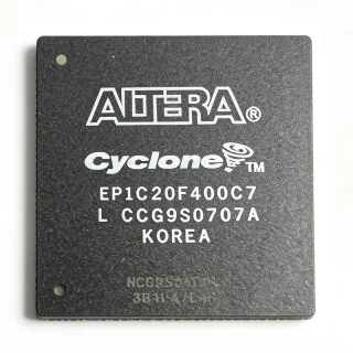
EP1C20F400C6N - Cyclone FPGA 20K LE BGA-400 | Intel
Teilenummer: EP1C20F400C6N ✗ Abgekündigt| Menge | Stückpreis | Gesamt |
|---|---|---|
| 1 | $78.5 | $78,50 |
| 10 | $72 | $720,00 |
| 100 | $64.5 | $6.450,00 |
| 500 | $58.25 | $29.125,00 |
| 1.000 | $53.1 | $53.100,00 |
EP1C20F400C6N Übersicht
An FPGA (Field Programmable Gate Array) is a semiconductor device whose digital logic functionality is defined after manufacturing via a configuration bitstream loaded into on-chip SRAM. FPGAs sit hierarchically as follows: programmable logic device -> FPGA -> SRAM-based FPGA -> low-cost FPGA. FPGAs are typically used when an application requires parallel processing, custom high-speed I/O, or hardware-level algorithm acceleration that fixed-function ASICs or microcontrollers cannot economically provide.
Key features of the EP1C20F400C6N include 20,060 logic elements, 294,912 bits of embedded RAM organized into M4K blocks, up to 301 user I/O pins, and a dedicated phase-locked loop (PLL) for clock management. The device supports multiple I/O standards including LVTTL, LVCMOS, SSTL, and LVDS, and includes embedded multipliers for DSP-style operations. Commercial temperature grade (0 °C to +85 °C) and 1.5 V core operation make it suitable for cost-sensitive consumer and industrial designs.
Architecturally, the Cyclone family uses a four-input look-up table (LUT) based logic element with embedded carry chains for arithmetic, distributed and block RAM, and a predictable routing fabric. Configuration is loaded via JTAG or an Altera configuration device (EPCS), and the Quartus II design software is the supported toolchain. The 400-ball BGA package offers high I/O density for complex glue-logic and parallel interface bridging.
Typical applications include digital video processing, industrial control logic, glue logic between processors and peripherals, custom interface bridging (e.g., parallel-to-parallel bus conversion), and low-volume ASIC prototyping. The large logic capacity makes it suitable for parallel data path implementations where microcontrollers would bottleneck.
When designing with the EP1C20F400C6N, ensure proper decoupling on every VCCINT and VCCIO supply pin per Altera's cyclone pin connection guidelines, and follow the IBIS model for high-speed signal integrity. Note that this device is now NRND/EOL: long-term designs should evaluate Cyclone II/III/IV successors.
This page synthesizes Intel datasheet specifications, distributor pricing, BGA-400 drop-in alternatives from the Cyclone family, and practical PCB layout guidance not found in a single distributor listing.
Drop-in-Alternativen für EP1C20F400C6N – gleiches Gehäuse, Pin-kompatibel. Bauteile mit anderem Gehäuse, die eine PCB-Überarbeitung erfordern, sind ausgeschlossen.
Varianten dieser Serie
Modelle derselben Serie, die drop-in-kompatibel sind mit EP1C20F400C6N (gleiche Bauform und Footprint) – abweichend in Speed Grade, Package, Process Technology, PLLs, Family.
Schnellvergleichstool – Wählen Sie Alternativbauteile für den Direktvergleich:
EP1C20F400C7N
✅ Drop-In✓ Auf Lager
$65.8 / Stück
Datenblatt ansehen →EP1C20F400C8N
✅ Drop-In✓ Auf Lager
$62.5 / Stück
Datenblatt ansehen →EP1C20F400I7N
✅ Drop-In✓ Auf Lager
$76.9 / Stück
Datenblatt ansehen →EP1C20F400C6
✅ Drop-In✓ Auf Lager
$18.95 / Stück
Datenblatt ansehen →EP1C20F400C6AB
✅ Drop-In✓ Auf Lager
$65.8 / Stück
Datenblatt ansehen →EP1C20F400C6AC
✅ Drop-In✓ Auf Lager
$52 / Stück
Datenblatt ansehen →EP1C20F400C6N Grenzwerte & elektrische Eigenschaften
| Family | Cyclone |
| Logic Elements | 20,060 |
| Total RAM Bits | 294,912 |
| User I/O Pins (max) | 301 |
| Gehäuse | 400-ball FineLine BGA (FBGA-400) |
| Package Dimensions | 21 x 21 mm |
| Ball Pitch | 1.0 mm |
| Core Voltage (VCCINT) | 1.5 V |
| Process Technology | 0.13 µm CMOS |
| Configuration Method | JTAG / Altera EPCS serial configuration device |
| PLL Count | 2 |
| Operating Temperature (Commercial) | 0 °C to +85 °C |
| Speed Grade | 6 (commercial, slower) |
| Montageart | Surface Mount |
EP1C20F400C6N 21 x 21 mm Pinbelegungsleitfaden
Pinbelegung für EP1C20F400C6N (21 x 21 mm-Gehäuse). Dieser digitale IC umfasst GPIO, Kommunikationsschnittstellen (UART, SPI, I2C) und Versorgungspins. Alternative Pin-Funktionen und Konfigurationsoptionen entnehmen Sie dem Herstellerdatenblatt. Unverzichtbar für Embedded-System-Design und PCB-Layout.

Keine detaillierten Pinbelegungsdaten verfügbar für EP1C20F400C6N.
Siehe die Datenblatt für die vollständige Pin-Konfiguration.
Typische Anwendungen
EP1C20F400C6N ist geeignet für 6 Anwendungs: Industrial Control Logic Board, Custom Parallel Interface Bridge, Digital Video Processing Pipeline, Low-Volume ASIC Prototyping, Test and Measurement Instrumentation Front-End, Legacy Hardware Maintenance / Repair Boards.
Industrial Control Logic Board
The EP1C20F400C6N is well-suited for industrial control logic boards requiring custom timing, parallel sensor interfaces, and deterministic response. Its 20,060 logic elements comfortably implement multi-axis motor control state machines, encoder interfaces, and safety logic that would otherwise require multiple discrete CPLDs. The 301 user I/O pins accommodate dozens of 24 V opto-isolated inputs, PWM outputs, and SPI/I2C master channels. Placed as the central logic device on a 4-layer FR4 PCB, the FBGA-400 package's 1.0 mm pitch requires standard SMT assembly with X-ray inspection for solder joint verification. Operating temperature 0 °C to +85 °C covers most factory floor environments; for harsher settings, choose the I7N industrial variant as a drop-in.
Empfohlen
Custom Parallel Interface Bridge
The EP1C20F400C6N excels at bridging legacy parallel buses (e.g., 16/32-bit SRAM-style interfaces) to modern memory-mapped or serial interfaces. With 20,060 logic elements, the device can implement full-width FIFOs, bus arbiters, and protocol converters simultaneously. The 301 user I/O count supports parallel data buses plus address, control, and handshake signals on a single device, eliminating multi-CPLD solutions. The 1.5 V VCCINT plus per-bank VCCIO allows mixed-voltage interfacing (3.3 V, 2.5 V, 1.8 V) without external level shifters. For designs migrating to lower-cost pin-compatible alternatives within the same family, EP1C20F400C8N provides timing margin for higher bus speeds.
Empfohlen
Digital Video Processing Pipeline
The EP1C20F400C6N is suitable for cost-sensitive digital video processing applications such as LCD monitor scalers, surveillance DVR front-ends, and industrial machine vision preprocessing. Its 20,060 logic elements support real-time scaling, color-space conversion, and basic image filtering at standard-definition rates. The two on-chip PLLs generate independent pixel clock domains for input capture and output display, simplifying multi-rate pipeline design. The 64 M4K memory blocks (294 Kbit total) buffer scan-line data efficiently. While modern designs often use dedicated video processors, the Cyclone remains viable for legacy or cost-constrained video products at SD resolutions.
Empfohlen
Low-Volume ASIC Prototyping
The EP1C20F400C6N serves as a pre-silicon validation platform for low-volume ASIC prototyping, particularly for designs targeting ~15K-20K gate equivalents. Engineers port RTL from Verilog or VHDL, verify functional correctness at system clock rates, and use the FPGA's JTAG-based logic analyzer (SignalTap) for debug before committing to mask costs. The 20K LE capacity closely matches mid-complexity ASICs in telecom, instrumentation, and industrial sensor processing. Once the design stabilizes, the same RTL can be re-targeted to an ASIC with minimal modification. This prototyping flow is documented in Altera's Quartus II design methodology guides.
Empfohlen
Test and Measurement Instrumentation Front-End
The EP1C20F400C6N is used in test and measurement instrumentation for custom waveform generation, protocol-aware triggering, and time-stamping logic where commercial ICs are unavailable. The 20K logic elements implement custom DSP blocks (FFT pre-processing, digital filters), while the 294 Kbit embedded RAM serves as deep sample buffers. The dedicated PLLs synchronize to external reference clocks (10 MHz, 100 MHz) for jitter-sensitive measurements. Combined with external high-speed ADCs, the Cyclone can implement a complete digitizer front-end. Its FBGA-400 footprint allows compact 4-channel T&M instruments where space is at a premium.
Empfohlen
Legacy Hardware Maintenance / Repair Boards
The EP1C20F400C6N is often used to manufacture replacement boards for legacy equipment where original FPGAs have failed or are obsolete. Because the Cyclone generation 1 is NRND but still available from distributors, repair technicians and aftermarket board builders can rebuild legacy designs without redesign. The exact same FBGA-400 footprint allows drop-in replacement of damaged originals, preserving PCB layout. Industrial, military, and aerospace systems with multi-decade service lives (e.g., avionics, satellite ground stations, factory automation from the 2000s) continue to depend on Cyclone-1 supply chains for sustainability.
Empfohlen
Zusammenfassung der empfohlenen Produkte
Technische Referenzdaten für EP1C20F400C6N – Vergleich, Designhinweise und Compliance-Informationen.
Auswahlhilfe
Vergleich mit Alternativen
| Parameter | Dieses Produkt | EP1C20F400C7N | EP1C20F400C8N | EP1C20F400I7N | EP1C20F400C6 |
|---|---|---|---|---|---|
| Package | FBGA-400 (21x21 mm, 1.0 mm pitch) | FBGA-400 (21x21 mm, 1.0 mm pitch) - same | FBGA-400 (21x21 mm, 1.0 mm pitch) - same | FBGA-400 (21x21 mm, 1.0 mm pitch) - same | FBGA-400 (21x21 mm, 1.0 mm pitch) - same |
| Brand | Intel (Altera) | Intel (Altera) - same | Intel (Altera) - same | Intel (Altera) - same | Intel (Altera) - same |
| Logic Elements | 20,060 | 20,060 | 20,060 | 20,060 | 20,060 |
| Speed Grade | C6 (commercial, slowest) | C7 (mid-speed) | C8 (fastest) | I7 (industrial temp, mid-speed) | C6 (identical to this product) |
| Temperature Grade | Commercial 0 °C to +85 °C | Commercial 0 °C to +85 °C | Commercial 0 °C to +85 °C | Industrial -40 °C to +100 °C | Commercial 0 °C to +85 °C |
| User I/O Pins | 301 | 301 | 301 | 301 | 301 |
| Embedded RAM | 294,912 bits (64 M4K blocks) | 294,912 bits | 294,912 bits | 294,912 bits | 294,912 bits |
| Lifecycle Status | NRND | NRND | NRND | NRND | NRND |
Wichtigste Unterscheidungsmerkmale
- Slowest commercial speed grade offers lowest cost (vs. EP1C20F400C8N)
- Commercial temperature grade suited for office/consumer products (vs. EP1C20F400I7N)
- Same-die alternative offers design flexibility (vs. EP1C20F400C6)
Designhinweise
The EP1C20F400C6N requires three supply rails: VCCINT (1.5 V core), VCCIO (per I/O bank, 3.3 V/2.5 V/1.8 V/1.5 V), and an analog PLL supply. Decoupling requirements per Altera's Cyclone Device Handbook: one 0.1 µF ceramic per VCCINT pin, one 33 µF bulk tantalum for VCCINT, and one 0.1 µF plus 10 µF per VCCIO bank. Estimated total bulk capacitance: ~200 µF across the supply network. Inadequate decoupling causes PLL jitter and intermittent configuration failures.
The FBGA-400 package has a 1.0 mm ball pitch and 21 x 21 mm body, requiring 4-layer or 6-layer PCB with via-in-pad or dog-bone fanout. Minimum trace width 0.1 mm (4 mil) with 0.1 mm spacing. All BGA balls must be X-ray inspected post-reflow; tombstoning on adjacent balls is a known assembly risk for 1.0 mm pitch. Use ENIG or OSP surface finish; HASL is not recommended for fine-pitch BGA. Reference: Cyclone Device Handbook, Chapter 4 PCB Layout Guidelines.
Configuration failure modes to avoid: (1) MSEL pins not strapped correctly for the chosen configuration scheme (AS, AP, PS, JTAG) - refer to Chapter 3 of the handbook. (2) CONF_DONE pin left floating; must be pulled up to VCCIO. (3) JTAG chain order errors when multiple devices share TDI/TDO. (4) Using Quartus Prime instead of legacy Quartus II, which does not support Cyclone generation 1. (5) VCCIO bank voltage mismatch when mixing 3.3 V and 1.8 V peripherals - each bank has independent VCCIO but shares GND.
Estimated: at 100% logic utilization with 200 MHz internal clock, typical Cyclone-1 core power dissipation is approximately 1.5-2.5 W. The FBGA-400 has theta_JA around 18-22 °C/W with proper PCB thermal via array under the package (per Altera thermal management guidelines). Without thermal vias, junction temperature can exceed 125 °C at high ambient. Recommended: place a 4x4 thermal via array (0.3 mm drill, 1.0 mm pitch) directly under the package BGA center pad to inner ground plane.
Compliance-Informationen
RoHS, REACH, lead-free, and halogen-free status not stated in the verified web snippets for this NRND part. Conflict minerals compliance assumed per Intel's corporate policy. AEC-Q100 not applicable: this is an FPGA, not an automotive-qualified IC.