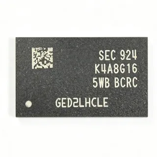
K9EUGY8S0M-BCK0 - Samsung V-NAND Flash Memory | Samsung
Teilenummer: K9EUGY8S0M-BCK0 ✓ Aktiv| Menge | Stückpreis | Gesamt |
|---|---|---|
| 1 | $0 | $0,00 |
| 10 | $0 | $0,00 |
| 100 | $0 | $0,00 |
| 500 | $0 | $0,00 |
| 1.000 | $0 | $0,00 |
K9EUGY8S0M-BCK0 Übersicht
NAND flash is a category of non-volatile memory that stores data in memory cells connected in series, enabling the highest bit density and lowest cost per gigabyte of any mainstream semiconductor memory technology. Within the memory hierarchy, NAND flash sits below DRAM in speed but retains data without power, making it the foundational technology for SSDs, eMMC, UFS, memory cards, and raw flash chips used in embedded systems.
K9-family V-NAND devices typically feature a standard asynchronous NAND interface with CE#, RE#, WE#, ALE, CLE, and I/O signals, support for block and page program/erase operations, and an on-chip page buffer. Samsung's V-NAND technology stacks memory cells vertically, increasing density while reducing cell-to-cell interference compared with planar NAND.
Raw NAND flash such as this device requires a host controller to manage wear leveling, bad-block management, and error-correcting code (ECC), which is essential for reliable long-term operation. Typical applications include embedded storage modules, industrial data recorders, set-top boxes, networking equipment, and solid-state drives.
When designing with raw NAND, verify the exact density, organization, voltage class, and speed grade from the official Samsung datasheet, because the part-number suffix system encodes many critical variations within the same base family. Pin-compatible family members often differ in capacity or speed grade only, which simplifies qualification of second sources within the same Samsung family.
This page consolidates verified distributor search data, Samsung-family cross-reference information, drop-in alternatives from the same K9 V-NAND family, and practical design guidance not found on typical catalog product pages.
Drop-in-Alternativen für K9EUGY8S0M-BCK0 – gleiches Gehäuse, Pin-kompatibel. Bauteile mit anderem Gehäuse, die eine PCB-Überarbeitung erfordern, sind ausgeschlossen.
Varianten dieser Serie
Modelle derselben Serie, die drop-in-kompatibel sind mit K9EUGY8S0M-BCK0 (gleiche Bauform und Footprint) – abweichend in Memory Type, Product Family, Mounting Type, Product Type, RoHS Status.
Schnellvergleichstool – Wählen Sie Alternativbauteile für den Direktvergleich:
K9DUGY8S0M-BCK0
✅ Drop-In✓ Auf Lager
Preis auf Anfrage
Datenblatt ansehen →K9DUGY8S0M-CCK0
✅ Drop-In✓ Auf Lager
Preis auf Anfrage
Datenblatt ansehen →K9CHGY8S5C-BCK0
✅ Drop-In✓ Auf Lager
Preis auf Anfrage
Datenblatt ansehen →K9CHGY8S5C-CCK0
✅ Drop-In✓ Auf Lager
Preis auf Anfrage
Datenblatt ansehen →K9HQGY8S5M
✅ Drop-In✓ Auf Lager
Preis auf Anfrage
Datenblatt ansehen →K9EUGY8S0M-BCK0 Grenzwerte & elektrische Eigenschaften
| Manufacturer | Samsung Electronics |
| Product Family | K9-series V-NAND Flash |
| Speichertyp | NAND Flash (non-volatile) |
| Montageart | Surface Mount |
K9EUGY8S0M-BCK0 standard Pinbelegungsleitfaden
Pinbelegung für K9EUGY8S0M-BCK0 (standard-Gehäuse). Dieser digitale IC umfasst GPIO, Kommunikationsschnittstellen (UART, SPI, I2C) und Versorgungspins. Alternative Pin-Funktionen und Konfigurationsoptionen entnehmen Sie dem Herstellerdatenblatt. Unverzichtbar für Embedded-System-Design und PCB-Layout.

Keine detaillierten Pinbelegungsdaten verfügbar für K9EUGY8S0M-BCK0.
Siehe die Datenblatt für die vollständige Pin-Konfiguration.
Typische Anwendungen
K9EUGY8S0M-BCK0 ist geeignet für 6 Anwendungs: Embedded Storage Modules, Industrial Data Recorders, Networking and Branch Equipment, Consumer Electronics and Set-Top Boxes, Solid-State Drive and Module Development, Service Provider Managed-Service Storage.
Embedded Storage Modules
Raw Samsung K9-family V-NAND such as the K9EUGY8S0M-BCK0 is the core storage element in custom embedded storage modules, where a host SoC or discrete NAND controller handles ECC, wear leveling, and bad-block management. The V-NAND vertical-stacking technology delivers high bit density in a compact FBGA surface-mount footprint, and the commodity NAND interface allows integration with a wide range of controllers. Designers should budget ECC strength according to the cell type stated in the Samsung datasheet and implement power-loss management, since interrupted program operations on raw NAND can corrupt the last written page without proper recovery firmware.
Empfohlen
Industrial Data Recorders
Industrial data loggers and recorders use high-density NAND flash to store sensor and process data across wide temperature ranges and long service lives. The K9EUGY8S0M-BCK0's V-NAND platform provides the storage capacity, while endurance is managed by the host FTL spreading writes across blocks per the program/erase cycle rating in the Samsung datasheet. For 24/7 logging, designers should size the flash bank so the sustained write rate stays well below the page program throughput limit, and should add brown-out detection or supercapacitor hold-up so the controller can complete in-flight page program operations when input power fails unexpectedly.
Empfohlen
Networking and Branch Equipment
Branch routers, switches, and gateways - the class of equipment represented by integrated services router platforms seen in the verified web data - require non-volatile storage for firmware images, configuration, and logging. A raw NAND device such as the K9EUGY8S0M-BCK0 provides low-cost gigabyte-class storage behind the system CPU's integrated flash controller, with dual-image firmware schemes relying on the NAND's page and block structure for safe over-the-air updates. Because networking equipment runs for years, firmware should monitor bad-block growth and reserve spare blocks; verify the factory bad-block marking scheme in the Samsung datasheet during the boot scan.
Empfohlen
Consumer Electronics and Set-Top Boxes
Set-top boxes, smart TVs, and streaming devices store firmware, channel databases, and recorded media on high-density NAND flash. The K9EUGY8S0M-BCK0 fits these cost-sensitive, high-volume applications where the SoC's built-in NAND controller and software FTL keep BOM cost low versus managed eMMC solutions. Designers should qualify the exact speed grade (BCK0 suffix) against the controller's supported NAND timing modes, since consumer SoCs often support only a subset of timing modes. Thermal conditions inside sealed consumer housings should also be reviewed against the operating temperature range in the Samsung datasheet.
Empfohlen
Solid-State Drive and Module Development
SSD controllers use multiple channels of raw NAND devices, and Samsung K9-family V-NAND parts are a standard building block for SSD and storage-module development. The K9EUGY8S0M-BCK0's commodity NAND interface lets an SSD controller interleave multiple devices across channels to aggregate bandwidth, while LDPC-based ECC compensates for the raw bit-error rate of high-density V-NAND. Prototype boards should provide per-device decoupling on the VCC/VCCQ rails and route the high-speed I/O and control signals with matched lengths; exact rail voltages and load capacitances must be taken from the official Samsung datasheet for this specific speed grade.
Empfohlen
Service Provider Managed-Service Storage
Customer-premises equipment deployed by service providers - including CPE gateways and managed-access devices - relies on reliable non-volatile storage for zero-touch provisioning images and telemetry logs. The K9EUGY8S0M-BCK0 provides commodity NAND storage whose cost and availability make it attractive for large deployments, and its Samsung family structure allows second-sourcing with the K9DUGY8S0M-BCK0 within the same PCB footprint, reducing supply-chain risk. Fleet firmware should implement dual-bank image storage with CRC verification on each boot, and provisioning tools should record the NAND READ ID to validate the fitted device against the approved vendor list.
Empfohlen
Zusammenfassung der empfohlenen Produkte
Technische Referenzdaten für K9EUGY8S0M-BCK0 – Vergleich, Designhinweise und Compliance-Informationen.
Auswahlhilfe
Vergleich mit Alternativen
| Parameter | Dieses Produkt | K9DUGY8S0M-BCK0 | K9DUGY8S0M-CCK0 | K9CHGY8S5C-BCK0 |
|---|---|---|---|---|
| Brand | Samsung | Samsung | Samsung | Samsung |
| Density Code | GY8S0M | GY8S0M - identical | GY8S0M - identical | GY8S5C - lower density |
| Product Generation | K9EU | K9DU - adjacent generation | K9DU - adjacent generation | K9CH - different generation |
| Speed / Packing Code | BCK0 | BCK0 - identical | CCK0 - different | BCK0 - identical |
| Lifecycle Status | Active (per family convention, verify) | Active (listed on XAIPART) | Active (listed on XAIPART) | Active (listed on XAIPART) |
Wichtigste Unterscheidungsmerkmale
- Identical density and package code to K9DUGY8S0M-BCK0 (vs. K9DUGY8S0M-BCK0)
- Full second-source coverage within one family (vs. K9CHGY8S5C-BCK0)
- Speed/packing code consistency (vs. K9DUGY8S0M-CCK0)
Designhinweise
Raw NAND devices typically require two supply rails (core VCC and I/O VCCQ); decouple each rail with at least a 100 nF ceramic capacitor placed within a few millimeters of each FBGA ball, plus bulk capacitance per rail at the bank level. Program and erase operations draw transient current bursts, so undersized decoupling shows up as voltage droop on VCC during tPROG, potentially corrupting in-flight operations. Confirm the exact rail voltages and capacitance recommendations from the official Samsung datasheet before tape-out, as these were not present in the verified web data.
FBGA-packaged NAND has fine-pitch balls requiring careful PCB escape routing. Keep the I/O bus, RE#, WE#, CLE, and ALE traces short and length-matched within the byte lane; route them over a continuous ground reference plane to minimize reflections and crosstalk. Avoid routing flash I/O adjacent to switching-regulator nodes or high-speed serial lines. When multiple NAND devices share a bus, keep stub lengths to individual devices short, and simulate or measure eye diagrams at the fastest supported NAND timing mode, not just at the default slow mode.
The most common raw-NAND design failures are (1) skipping the factory bad-block scan at first boot - every NAND ships with some marked bad blocks that the FTL must remap; (2) ECC weaker than required for the cell type, causing uncorrectable bit errors as the device ages; and (3) assuming different K9-family generations are identical - the K9DU and K9EU parts differ in cell type or generation, so always re-validate READ ID responses, ONFI timing modes, and datasheet AC parameters when substituting family members, even when the package footprint is identical.
Compliance-Informationen
Compliance data was not present in the verified web data retrieved on 2026-09-04. Obtain the official Samsung material declaration and compliance certificates before use in regulated products.