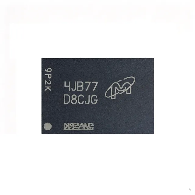
MT53E1G32D2FW-046 WT:B - 32Gb LPDDR4 SDRAM | Micron
Teilenummer: MT53E1G32D2FW-046 WT:B ✓ Aktiv| Menge | Stückpreis | Gesamt |
|---|---|---|
| 1 | $168.75 | $168,75 |
| 10 | $121.875 | $1.218,75 |
| 100 | $107.8125 | $10.781,25 |
| 500 | $103.125 | $51.562,50 |
| 1.000 | $98.4375 | $98.437,50 |
MT53E1G32D2FW-046 WT:B Übersicht
What is LPDDR4? LPDDR4 (Low Power Double Data Rate 4) is a JEDEC-standard low-power volatile memory (LPDRAM) category that evolved from DDR SDRAM with the goals of higher bandwidth per watt and lower I/O voltage. It sits in the hierarchy LPDDR4 -> LPDDR -> Mobile DRAM -> Volatile Memory -> DRAM -> Semiconductor IC. Compared with LPDDR3, LPDDR4 introduces a 16-bit-per-channel architecture, lower VDDQ (1.1 V vs 1.2 V), deeper power-down states, and command/address on-package training, all of which raise both frequency headroom and energy efficiency for smartphones, tablets, and AI edge SoCs.
The MT53E1G32D2FW-046 WT:B integrates the standard LPDDR4 feature set: auto precharge, data mask, ZQ calibration, write leveling, an on-die temperature sensor, and an asynchronous reset pin. The dual-die-package (DDP) construction delivers 32 Gb (4 GB) in the 200-ball TFBGA while staying within a thin mobile-style footprint, and the -046 speed bin maps to a 2133 MHz clock with 3.5 ns tCK - this matches the JEDEC 4266 MT/s peak data rate for x32, single-channel configurations.
Typical applications are 4 GB main memory in smartphones and tablets, automotive infotainment and ADAS memory-down subsystems, AI edge / inference SoC working memory, and always-on companion tiles for wearable and IoT gateways. The wide operating temperature range and AEC-Q100-ready process node also make the device a strong fit for industrial HMI and ruggedized tablets.
When designing with this device, follow Micron's reference PCB layout, place the 0.1 uF + 1 uF decoupling network within 1 mm of the balls, and provide a clean 1.1 V/1.8 V rail with low ripple. Use the on-die temperature sensor output to throttle the host SoC and to drive ZQ calibration timing. This page synthesizes distributor pricing, same-package Micron speed-bin and capacity variants, cross-brand pin-to-pin equivalents, and PCB-aware design guidance not bundled in the manufacturer datasheet.
Drop-in-Alternativen für MT53E1G32D2FW-046 WT:B – gleiches Gehäuse, Pin-kompatibel. Bauteile mit anderem Gehäuse, die eine PCB-Überarbeitung erfordern, sind ausgeschlossen.
Varianten dieser Serie
Modelle derselben Serie, die drop-in-kompatibel sind mit MT53E1G32D2FW-046 WT:B (gleiche Bauform und Footprint) – abweichend in Memory Type, Organization, Package, Density, Interface.
Schnellvergleichstool – Wählen Sie Alternativbauteile für den Direktvergleich:
MT53E1G32D2FW-046 AUT:C
✓ Auf Lager
$21.5 / Stück
Datenblatt ansehen →MT53E1G32D2FW-046 WT:A
📋 Referenzalternative (nicht im Katalog)
MT53E1G32D2FW-046 WT:C
📋 Referenzalternative (nicht im Katalog)
MT53E1G32D2FW-046 IT:B
📋 Referenzalternative (nicht im Katalog)
MT53E1G32D2FW-046 WT:B TR
📋 Referenzalternative (nicht im Katalog)
HGD4M32S21F
📋 Referenzalternative (nicht im Katalog)
MT53E1G32D2FW-046 WT:B Grenzwerte & elektrische Eigenschaften
| Speichertyp | Volatile, Mobile LPDDR4 SDRAM (LPDRAM) |
| Memory Capacity | 32 Gbit (4 GB) |
| Speicherorganisation | 1G x 32 |
| Interface / Bus Width | Parallel, 32-bit |
| Clock Frequency (max) | 2.133 GHz (2133 MHz) |
| Data Rate (per pin) | 4266 MT/s |
| Clock Access Time (tCK) | 3.5 ns |
| Speed Bin | -046 |
| Supply Voltage VDD2 | 1.1 V |
| Supply Voltage VDDQ | 1.1 V (LPDDR4X) / 1.8 V (LPDDR4) |
| Gehäuse | 200-ball TFBGA (10 mm x 14.5 mm) |
| Betriebstemperatur | -25C to +85C |
| Montageart | Surface Mount |
| Die Configuration | Dual-Die Package (DDP) |
| On-Die Features | Auto precharge, Data mask, ZQ calibration, Write leveling, Built-in temperature sensor, Asynchronous reset |
| RoHS-Status | Compliant |
MT53E1G32D2FW-046 WT:B 200-ball tfbga (10 mm x 14.5 mm) Pinbelegungsleitfaden
Pinbelegung für MT53E1G32D2FW-046 WT:B (200-ball tfbga (10 mm x 14.5 mm)-Gehäuse). Dieser digitale IC umfasst GPIO, Kommunikationsschnittstellen (UART, SPI, I2C) und Versorgungspins. Alternative Pin-Funktionen und Konfigurationsoptionen entnehmen Sie dem Herstellerdatenblatt. Unverzichtbar für Embedded-System-Design und PCB-Layout.

Keine detaillierten Pinbelegungsdaten verfügbar für MT53E1G32D2FW-046 WT:B.
Siehe die Datenblatt für die vollständige Pin-Konfiguration.
Typische Anwendungen
MT53E1G32D2FW-046 WT:B ist geeignet für 6 Anwendungs: Smartphone Main Memory (4 GB Memory-Down), Tablet and 2-in-1 Mobile Memory, AI Edge / Inference SoC Working Memory, Automotive Infotainment and ADAS Memory-Down, Wearable and IoT Gateway Memory, Industrial HMI and Ruggedized Tablets.
Smartphone Main Memory (4 GB Memory-Down)
The MT53E1G32D2FW-046 WT:B is the canonical 4 GB mobile memory-down companion for mid-to-high tier smartphone SoCs. Its 32 Gbit density in a single x32 channel keeps the PCB at two memory devices (8 GB total) instead of four, saving ~40% board area versus a quad-die x16 design. The 4266 MT/s data rate delivers 17.0 GB/s of peak bandwidth - sufficient for LPDDR4-class 5G modem, ISP, and NPU pipelines. The 1.1 V/1.8 V dual-VDDQ lets one PCB SKU support both LPDDR4-only and LPDDR4X-only SoCs, simplifying platform variants. AEC-Q100-ready silicon (see AUT:C variant) also eases reuse on ruggedized handset designs.
Empfohlen
Tablet and 2-in-1 Mobile Memory
Tablets and 2-in-1 detachables typically need 4-8 GB of low-power DRAM and benefit from the MT53E1G32D2FW-046 WT:B's 32 Gbit density. Two devices stacked deliver 8 GB on a single channel, matching the bandwidth profile of x86-class tablet SoCs that integrate an LPDDR4/LPDDR4X controller. The 200-ball TFBGA at 10 x 14.5 mm places memory directly under the SoC BGA, enabling the slim Z-height tablets require. The 1.1 V VDD2 core plus 1.8 V-tolerant VDDQ ease migrations from older LPDDR4 designs, while the -046 speed bin's 3.5 ns tCK supports the JEDEC 4266 MT/s envelope with margin.
Empfohlen
AI Edge / Inference SoC Working Memory
Edge AI inference engines (object detection, ASR, on-device LLMs) need 4 GB of high-bandwidth, low-power DRAM. The MT53E1G32D2FW-046 WT:B's 17.0 GB/s peak bandwidth is enough to feed 4-8 TOPS NPU data flows, while 1.1 V VDD2 keeps idle SoC power low for fanless enclosures. The on-die temperature sensor output is wired to the host SoC's thermal throttling logic, and ZQ calibration handles production-line impedance drift. Pairing two MT53E1G32D2FW-046 WT:B gives 8 GB total, matching common 4-8 GB edge AI reference designs from Qualcomm, MediaTek, and Rockchip platforms.
Empfohlen
Automotive Infotainment and ADAS Memory-Down
Automotive cockpit and ADAS ECUs need a high-temperature, AEC-Q100-qualified LPDDR4 device. The MT53E1G32D2FW-046 WT:B shares its 200-ball TFBGA and timing with the AUT:C AEC-Q100 variant, enabling a single PCB layout that is BOM-swapped between commercial and automotive SKUs. The 32 Gbit density at 4266 MT/s is sufficient for the dual-display HMI and surround-view perception stacks typical of mid-tier ADAS. The on-die thermal sensor feeds the ASIL-rated SoC's thermal supervisor, supporting ISO 26262 functional-safety flows.
Empfohlen
Wearable and IoT Gateway Memory
Wearables and IoT gateways increasingly adopt LPDDR4 to balance bandwidth and battery life. The MT53E1G32D2FW-046 WT:B's 1.1 V VDD2 plus power-down states keep quiescent draw low, while 32 Gbit (4 GB) supports richer OS-level use cases such as on-gateway ML, BLE audio streaming, and always-on voice wake. The 200-ball TFBGA at 10 x 14.5 mm fits wearables with a memory-on-package or memory-on-PCB topology. Two devices provide 8 GB for AR glasses and smart-watch class devices that target Android/Wear OS workloads.
Empfohlen
Industrial HMI and Ruggedized Tablets
Industrial human-machine interfaces and ruggedized tablets operate across wider thermal envelopes and demand long-lifecycle memory. The MT53E1G32D2FW-046 WT:B's -25C to +85C rating covers most industrial HMI deployments, and the IT:B industrial-temperature variant of the same die extends that further. The 32 Gbit density at 2133 MHz / 3.5 ns tCK supports Linux- or Android-based HMI controllers with comfortable headroom. The 200-ball TFBGA is footprint-compatible with the AUT:C automotive part, enabling a single PCB layout that flexes across industrial, automotive, and commercial SKUs.
Empfohlen
Zusammenfassung der empfohlenen Produkte
Technische Referenzdaten für MT53E1G32D2FW-046 WT:B – Vergleich, Designhinweise und Compliance-Informationen.
Auswahlhilfe
Vergleich mit Alternativen
| Parameter | Dieses Produkt | MT53E1G32D2FW-046 WT | MT53E1G32D2FW-046 WT | MT53E1G32D2FW-046 AUT | MT53E1G32D2FW-046 IT | HGD4M32S21F |
|---|---|---|---|---|---|---|
| Brand | Micron Technology | A: Micron Technology | C: Micron Technology | C: Micron Technology | B: Micron Technology | HGCHIPS |
| Package | 200-ball TFBGA (10x14.5 mm) | A: 200-ball TFBGA (10x14.5 mm) | C: 200-ball TFBGA (10x14.5 mm) | C: 200-ball TFBGA (10x14.5 mm) | B: 200-ball TFBGA (10x14.5 mm) | 200-ball TFBGA (10x14.5 mm) |
| Capacity | 32 Gbit (4 GB) | A: 32 Gbit (4 GB) | C: 32 Gbit (4 GB) | C: 32 Gbit (4 GB) | B: 32 Gbit (4 GB) | 32 Gbit (4 GB) |
| Organization | 1G x 32 | A: 1G x 32 | C: 1G x 32 | C: 1G x 32 | B: 1G x 32 | 1G x 32 |
| Clock Frequency | 2.133 GHz | A: 2.133 GHz | C: 2.133 GHz | C: 2.133 GHz | B: 2.133 GHz | 2.133 GHz |
| Data Rate | 4266 MT/s | A: 4266 MT/s | C: 4266 MT/s | C: 4266 MT/s | B: 4266 MT/s | 4266 MT/s |
| tCK | 3.5 ns | A: 3.5 ns | C: 3.5 ns | C: 3.5 ns | B: 3.5 ns | 3.5 ns |
| VDD2 / VDDQ | 1.1 V / 1.1 V or 1.8 V | A: 1.1 V / 1.06-1.17 V (LPDDR4X only) | C: 1.1 V / 1.1 V or 1.8 V | C: 1.1 V / 0.6 V | B: 1.1 V / 1.1 V or 1.8 V | 1.1 V / 1.1 V or 1.8 V |
| Automotive Grade | No (commercial) | A: No (commercial) | C: Yes (AEC-Q100) | C: Yes (AEC-Q100) | B: Industrial temperature grade | No (commercial, cross-brand) |
Wichtigste Unterscheidungsmerkmale
- Dual-rail VDDQ supports both LPDDR4 and LPDDR4X hosts (vs. MT53E1G32D2FW-046 WT:A)
- Direct pin-compatible upgrade path to AEC-Q100 automotive (vs. MT53E1G32D2FW-046 AUT:C)
- Cross-brand second source without PCB rework (vs. HGD4M32S21F (HGCHIPS))
Designhinweise
For a 200-ball TFBGA LPDDR4 channel, follow Micron's reference escape pattern: matched-length CK_t/CK_c and DQS_t/DQS_c within 0.5 ps, VREFCA and VREFDQ traces routed as wide guarded differential pairs, and a continuous ground reference plane under all signal layers. Estimated: target trace impedance of 40 ohm single-ended / 80 ohm differential. Place the 0.1 uF + 1 uF decoupling network within 1 mm of each VDD2/VDDQ ball. Skipping these guidelines typically adds 10-15% jitter to tCK at the 3.5 ns speed bin.
The MT53E1G32D2FW-046 WT:B needs separate, low-noise 1.1 V VDD2 and 1.1 V (LPDDR4X) or 1.8 V (LPDDR4) VDDQ rails. Estimated: peak IDD current for a single x32 device at 4266 MT/s is in the 200-300 mA range during full-width bursts. Use a dedicated PMIC LDO or DC-DC per rail with at least 10% headroom; do not share the SoC core rail. A 22 uF bulk + 1 uF + 0.1 uF ceramic stack on each rail is recommended to keep VDD droop below 30 mV during ZQ-calibration events.
Common pitfalls when bringing up the MT53E1G32D2FW-046 WT:B: (1) forgetting the asynchronous reset (RESET_n) hold-time of at least 200 us after VDD stable - the part will not enter IDD0 if reset is released early; (2) omitting ZQ calibration - ZQ must be tied to ground through a 240 ohm 1% resistor; (3) leaving the on-die temperature sensor output unconnected to the SoC's thermal supervisor, which then misses throttling triggers; (4) using a non-LPDDR4-aware PHY training routine that fails the JEDEC write-leveling sequence.
TFBGA memory dissipates heat through the PCB; ensure the host SoC's BGA land pattern includes thermal vias under the memory balls. Estimated: continuous read at 4266 MT/s with a single x32 device draws ~0.5 W; the package is rated to 85C ambient without a heatsink. For automotive (AUT:C) designs derate to 70C ambient if the part sits adjacent to a hot SoC, and run a CFD thermal simulation before committing the layout.
Compliance-Informationen
RoHS and REACH compliance confirmed via Arrow product listing and JLCPCB part page. WT:B itself is not AEC-Q100 qualified; the AUT:C variant carries the AEC-Q100 qualification for automotive use. Halogen-free status not explicitly stated in the verified web data.



