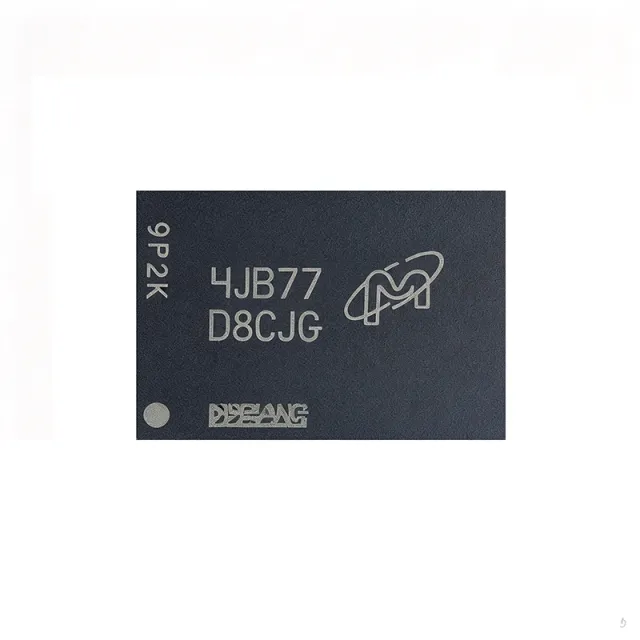
MT53E1G32D2FW-046 WT:B - 32Gb LPDDR4 SDRAM | Micron
MPN: MT53E1G32D2FW-046 WT:B ✓ Active| Qty | Unit Price | Extended |
|---|---|---|
| 1 | $168.75 | $168.75 |
| 10 | $121.875 | $1,218.75 |
| 100 | $107.8125 | $10,781.25 |
| 500 | $103.125 | $51,562.50 |
| 1,000 | $98.4375 | $98,437.50 |
MT53E1G32D2FW-046 WT:B Overview
What is LPDDR4? LPDDR4 (Low Power Double Data Rate 4) is a JEDEC-standard low-power volatile memory (LPDRAM) category that evolved from DDR SDRAM with the goals of higher bandwidth per watt and lower I/O voltage. It sits in the hierarchy LPDDR4 -> LPDDR -> Mobile DRAM -> Volatile Memory -> DRAM -> Semiconductor IC. Compared with LPDDR3, LPDDR4 introduces a 16-bit-per-channel architecture, lower VDDQ (1.1 V vs 1.2 V), deeper power-down states, and command/address on-package training, all of which raise both frequency headroom and energy efficiency for smartphones, tablets, and AI edge SoCs.
The MT53E1G32D2FW-046 WT:B integrates the standard LPDDR4 feature set: auto precharge, data mask, ZQ calibration, write leveling, an on-die temperature sensor, and an asynchronous reset pin. The dual-die-package (DDP) construction delivers 32 Gb (4 GB) in the 200-ball TFBGA while staying within a thin mobile-style footprint, and the -046 speed bin maps to a 2133 MHz clock with 3.5 ns tCK - this matches the JEDEC 4266 MT/s peak data rate for x32, single-channel configurations.
Typical applications are 4 GB main memory in smartphones and tablets, automotive infotainment and ADAS memory-down subsystems, AI edge / inference SoC working memory, and always-on companion tiles for wearable and IoT gateways. The wide operating temperature range and AEC-Q100-ready process node also make the device a strong fit for industrial HMI and ruggedized tablets.
When designing with this device, follow Micron's reference PCB layout, place the 0.1 uF + 1 uF decoupling network within 1 mm of the balls, and provide a clean 1.1 V/1.8 V rail with low ripple. Use the on-die temperature sensor output to throttle the host SoC and to drive ZQ calibration timing. This page synthesizes distributor pricing, same-package Micron speed-bin and capacity variants, cross-brand pin-to-pin equivalents, and PCB-aware design guidance not bundled in the manufacturer datasheet.
Drop-in alternatives for MT53E1G32D2FW-046 WT:B — same package, pin-to-pin compatible. Different-package parts requiring PCB rework are excluded.
Variants in this series
Same-series models that are drop-in compatible with MT53E1G32D2FW-046 WT:B (same form factor and footprint) — differing in Memory Type, Organization, Package, Density, Interface.
Quick Comparison Tool — Select alternative parts for side-by-side comparison:
MT53E1G32D2FW-046 AUT:C
✓ In Stock
$21.5 / Unit
View Datasheet →MT53E1G32D2FW-046 WT:A
📋 Reference alternative (not in catalog)
MT53E1G32D2FW-046 WT:C
📋 Reference alternative (not in catalog)
MT53E1G32D2FW-046 IT:B
📋 Reference alternative (not in catalog)
MT53E1G32D2FW-046 WT:B TR
📋 Reference alternative (not in catalog)
HGD4M32S21F
📋 Reference alternative (not in catalog)
MT53E1G32D2FW-046 WT:B Maximum Ratings & Electrical Characteristics
| Memory Type | Volatile, Mobile LPDDR4 SDRAM (LPDRAM) |
| Memory Capacity | 32 Gbit (4 GB) |
| Organization | 1G x 32 |
| Interface / Bus Width | Parallel, 32-bit |
| Clock Frequency (max) | 2.133 GHz (2133 MHz) |
| Data Rate (per pin) | 4266 MT/s |
| Clock Access Time (tCK) | 3.5 ns |
| Speed Bin | -046 |
| Supply Voltage VDD2 | 1.1 V |
| Supply Voltage VDDQ | 1.1 V (LPDDR4X) / 1.8 V (LPDDR4) |
| Package | 200-ball TFBGA (10 mm x 14.5 mm) |
| Operating Temperature | -25C to +85C |
| Mounting Type | Surface Mount |
| Die Configuration | Dual-Die Package (DDP) |
| On-Die Features | Auto precharge, Data mask, ZQ calibration, Write leveling, Built-in temperature sensor, Asynchronous reset |
| RoHS Status | Compliant |
MT53E1G32D2FW-046 WT:B 200-ball tfbga (10 mm x 14.5 mm) Pin Configuration Guide
Pin configuration for MT53E1G32D2FW-046 WT:B (200-ball tfbga (10 mm x 14.5 mm) package). This digital IC includes GPIO, communication interfaces (UART, SPI, I2C), and power pins. Refer to the manufacturer datasheet for alternate pin functions and configuration options. Essential for embedded system design and PCB layout.

No detailed pinout data available for MT53E1G32D2FW-046 WT:B.
Refer to the datasheet for full pin configuration.
Typical Applications
MT53E1G32D2FW-046 WT:B is suitable for 6 applications: Smartphone Main Memory (4 GB Memory-Down), Tablet and 2-in-1 Mobile Memory, AI Edge / Inference SoC Working Memory, Automotive Infotainment and ADAS Memory-Down, Wearable and IoT Gateway Memory, Industrial HMI and Ruggedized Tablets.
Smartphone Main Memory (4 GB Memory-Down)
The MT53E1G32D2FW-046 WT:B is the canonical 4 GB mobile memory-down companion for mid-to-high tier smartphone SoCs. Its 32 Gbit density in a single x32 channel keeps the PCB at two memory devices (8 GB total) instead of four, saving ~40% board area versus a quad-die x16 design. The 4266 MT/s data rate delivers 17.0 GB/s of peak bandwidth - sufficient for LPDDR4-class 5G modem, ISP, and NPU pipelines. The 1.1 V/1.8 V dual-VDDQ lets one PCB SKU support both LPDDR4-only and LPDDR4X-only SoCs, simplifying platform variants. AEC-Q100-ready silicon (see AUT:C variant) also eases reuse on ruggedized handset designs.
Recommended
Tablet and 2-in-1 Mobile Memory
Tablets and 2-in-1 detachables typically need 4-8 GB of low-power DRAM and benefit from the MT53E1G32D2FW-046 WT:B's 32 Gbit density. Two devices stacked deliver 8 GB on a single channel, matching the bandwidth profile of x86-class tablet SoCs that integrate an LPDDR4/LPDDR4X controller. The 200-ball TFBGA at 10 x 14.5 mm places memory directly under the SoC BGA, enabling the slim Z-height tablets require. The 1.1 V VDD2 core plus 1.8 V-tolerant VDDQ ease migrations from older LPDDR4 designs, while the -046 speed bin's 3.5 ns tCK supports the JEDEC 4266 MT/s envelope with margin.
Recommended
AI Edge / Inference SoC Working Memory
Edge AI inference engines (object detection, ASR, on-device LLMs) need 4 GB of high-bandwidth, low-power DRAM. The MT53E1G32D2FW-046 WT:B's 17.0 GB/s peak bandwidth is enough to feed 4-8 TOPS NPU data flows, while 1.1 V VDD2 keeps idle SoC power low for fanless enclosures. The on-die temperature sensor output is wired to the host SoC's thermal throttling logic, and ZQ calibration handles production-line impedance drift. Pairing two MT53E1G32D2FW-046 WT:B gives 8 GB total, matching common 4-8 GB edge AI reference designs from Qualcomm, MediaTek, and Rockchip platforms.
Recommended
Automotive Infotainment and ADAS Memory-Down
Automotive cockpit and ADAS ECUs need a high-temperature, AEC-Q100-qualified LPDDR4 device. The MT53E1G32D2FW-046 WT:B shares its 200-ball TFBGA and timing with the AUT:C AEC-Q100 variant, enabling a single PCB layout that is BOM-swapped between commercial and automotive SKUs. The 32 Gbit density at 4266 MT/s is sufficient for the dual-display HMI and surround-view perception stacks typical of mid-tier ADAS. The on-die thermal sensor feeds the ASIL-rated SoC's thermal supervisor, supporting ISO 26262 functional-safety flows.
Recommended
Wearable and IoT Gateway Memory
Wearables and IoT gateways increasingly adopt LPDDR4 to balance bandwidth and battery life. The MT53E1G32D2FW-046 WT:B's 1.1 V VDD2 plus power-down states keep quiescent draw low, while 32 Gbit (4 GB) supports richer OS-level use cases such as on-gateway ML, BLE audio streaming, and always-on voice wake. The 200-ball TFBGA at 10 x 14.5 mm fits wearables with a memory-on-package or memory-on-PCB topology. Two devices provide 8 GB for AR glasses and smart-watch class devices that target Android/Wear OS workloads.
Recommended
Industrial HMI and Ruggedized Tablets
Industrial human-machine interfaces and ruggedized tablets operate across wider thermal envelopes and demand long-lifecycle memory. The MT53E1G32D2FW-046 WT:B's -25C to +85C rating covers most industrial HMI deployments, and the IT:B industrial-temperature variant of the same die extends that further. The 32 Gbit density at 2133 MHz / 3.5 ns tCK supports Linux- or Android-based HMI controllers with comfortable headroom. The 200-ball TFBGA is footprint-compatible with the AUT:C automotive part, enabling a single PCB layout that flexes across industrial, automotive, and commercial SKUs.
Recommended
Recommended Products Summary
Engineering reference data for MT53E1G32D2FW-046 WT:B — comparison, design guidance, and compliance information.
Selection Guide
Comparison with Alternatives
| Parameter | This Product | MT53E1G32D2FW-046 WT | MT53E1G32D2FW-046 WT | MT53E1G32D2FW-046 AUT | MT53E1G32D2FW-046 IT | HGD4M32S21F |
|---|---|---|---|---|---|---|
| Brand | Micron Technology | A: Micron Technology | C: Micron Technology | C: Micron Technology | B: Micron Technology | HGCHIPS |
| Package | 200-ball TFBGA (10x14.5 mm) | A: 200-ball TFBGA (10x14.5 mm) | C: 200-ball TFBGA (10x14.5 mm) | C: 200-ball TFBGA (10x14.5 mm) | B: 200-ball TFBGA (10x14.5 mm) | 200-ball TFBGA (10x14.5 mm) |
| Capacity | 32 Gbit (4 GB) | A: 32 Gbit (4 GB) | C: 32 Gbit (4 GB) | C: 32 Gbit (4 GB) | B: 32 Gbit (4 GB) | 32 Gbit (4 GB) |
| Organization | 1G x 32 | A: 1G x 32 | C: 1G x 32 | C: 1G x 32 | B: 1G x 32 | 1G x 32 |
| Clock Frequency | 2.133 GHz | A: 2.133 GHz | C: 2.133 GHz | C: 2.133 GHz | B: 2.133 GHz | 2.133 GHz |
| Data Rate | 4266 MT/s | A: 4266 MT/s | C: 4266 MT/s | C: 4266 MT/s | B: 4266 MT/s | 4266 MT/s |
| tCK | 3.5 ns | A: 3.5 ns | C: 3.5 ns | C: 3.5 ns | B: 3.5 ns | 3.5 ns |
| VDD2 / VDDQ | 1.1 V / 1.1 V or 1.8 V | A: 1.1 V / 1.06-1.17 V (LPDDR4X only) | C: 1.1 V / 1.1 V or 1.8 V | C: 1.1 V / 0.6 V | B: 1.1 V / 1.1 V or 1.8 V | 1.1 V / 1.1 V or 1.8 V |
| Automotive Grade | No (commercial) | A: No (commercial) | C: Yes (AEC-Q100) | C: Yes (AEC-Q100) | B: Industrial temperature grade | No (commercial, cross-brand) |
Key Differentiators
- Dual-rail VDDQ supports both LPDDR4 and LPDDR4X hosts (vs MT53E1G32D2FW-046 WT:A)
- Direct pin-compatible upgrade path to AEC-Q100 automotive (vs MT53E1G32D2FW-046 AUT:C)
- Cross-brand second source without PCB rework (vs HGD4M32S21F (HGCHIPS))
Design Notes
For a 200-ball TFBGA LPDDR4 channel, follow Micron's reference escape pattern: matched-length CK_t/CK_c and DQS_t/DQS_c within 0.5 ps, VREFCA and VREFDQ traces routed as wide guarded differential pairs, and a continuous ground reference plane under all signal layers. Estimated: target trace impedance of 40 ohm single-ended / 80 ohm differential. Place the 0.1 uF + 1 uF decoupling network within 1 mm of each VDD2/VDDQ ball. Skipping these guidelines typically adds 10-15% jitter to tCK at the 3.5 ns speed bin.
The MT53E1G32D2FW-046 WT:B needs separate, low-noise 1.1 V VDD2 and 1.1 V (LPDDR4X) or 1.8 V (LPDDR4) VDDQ rails. Estimated: peak IDD current for a single x32 device at 4266 MT/s is in the 200-300 mA range during full-width bursts. Use a dedicated PMIC LDO or DC-DC per rail with at least 10% headroom; do not share the SoC core rail. A 22 uF bulk + 1 uF + 0.1 uF ceramic stack on each rail is recommended to keep VDD droop below 30 mV during ZQ-calibration events.
Common pitfalls when bringing up the MT53E1G32D2FW-046 WT:B: (1) forgetting the asynchronous reset (RESET_n) hold-time of at least 200 us after VDD stable - the part will not enter IDD0 if reset is released early; (2) omitting ZQ calibration - ZQ must be tied to ground through a 240 ohm 1% resistor; (3) leaving the on-die temperature sensor output unconnected to the SoC's thermal supervisor, which then misses throttling triggers; (4) using a non-LPDDR4-aware PHY training routine that fails the JEDEC write-leveling sequence.
TFBGA memory dissipates heat through the PCB; ensure the host SoC's BGA land pattern includes thermal vias under the memory balls. Estimated: continuous read at 4266 MT/s with a single x32 device draws ~0.5 W; the package is rated to 85C ambient without a heatsink. For automotive (AUT:C) designs derate to 70C ambient if the part sits adjacent to a hot SoC, and run a CFD thermal simulation before committing the layout.
Compliance Information
RoHS and REACH compliance confirmed via Arrow product listing and JLCPCB part page. WT:B itself is not AEC-Q100 qualified; the AUT:C variant carries the AEC-Q100 qualification for automotive use. Halogen-free status not explicitly stated in the verified web data.



