Productos (38.000+)

W29EE011P-90 - 1Mb 5V Parallel Flash, 90ns, 32-PLCC | Winbond
W29EE011P-90

W29EE011P-90 - 1Mb 5V Parallel Flash, 90ns, 32-PLCC | Winbond

The Winbond W29EE011P-90 is a 1-megabit (128K x 8) CMOS parallel flash memory with 90 ns access time, organized as 128K bytes and packaged in a 32-pin PLCC. It operates from a single 5V supply and supports in-system program and erase operations without requiring a 12V VPP. A flash memory is a non-volatile storage technology that retains data when power is removed and supports electrical erase and program cycles in circuit. The W29EE011P-90 sits within the memory IC hierarchy as a parallel NOR flash, distinct from serial SPI flash (fewer pins, lower pin count) and NAND flash (higher density, page/block oriented). Parallel NOR flash is the legacy choice for code storage in 8-bit and 16-bit microcontrollers, EPROM replacement, and firmware boot ROMs where byte-level random access and simple bus interface are required. The W29EE011P-90 features 90 ns maximum access time, sector/chip erase capability, and CMOS low-power operation. It is designed as a drop-in replacement for legacy 5V EPROMs and standard 1-Mbit flash devices. The 32-PLCC package provides a JEDEC-standard pinout compatible with the industry 1-Mbit parallel flash footprint, simplifying board-level migration from older AMD/Atmel/ST 28F001 or 29EE011 sockets. Typical applications include embedded firmware storage for industrial controllers, legacy 8051/68HC11/MCS-96 system boot memory, BIOS and firmware update banks, point-of-sale terminals, and industrial PLC code storage. The 90 ns access time supports microcontrollers running at up to approximately 8 MHz without wait states. When designing with this part, note that the 32-PLCC package requires a PLCC socket or careful reflow profile for surface-mount assembly. Verify the device's command set (byte programming, sector erase, chip erase) against your firmware's flash algorithm before substitution. The part is suitable for 5V-only systems; it does not support 3.3V operation.

Cotización Contacto
W29N01HVBINF - 1Gbit 3V SLC NAND Flash 63-VFBGA | Winbond
W29N01HVBINF

W29N01HVBINF - 1Gbit 3V SLC NAND Flash 63-VFBGA | Winbond

The Winbond W29N01HVBINF is a 1 Gbit (128 M x 8) Single-Level Cell (SLC) NAND Flash memory organized as 1024 blocks of 64 KB each, supplied in a compact 63-ball VFBGA (9 mm x 11 mm) package. It operates from a single 3.0 V power supply (2.7 V to 3.6 V) and provides asynchronous x8 parallel I/O with typical page-read access of 25 ns, making it well suited for embedded code and data storage where reliability and endurance matter more than raw throughput. NAND Flash is a non-volatile memory technology that stores bits as charge on a floating-gate MOSFET cell. SLC NAND stores one bit per cell, which delivers 10x the endurance and 10x the data retention of MLC or TLC NAND at the cost of lower density per die. Within the storage taxonomy, NAND Flash sits below NOR Flash for code execution and below DRAM for volatile working memory, but above raw EEPROM in density-per-area. The 1 Gbit SLC class targets boot-loaders, firmware images, and transaction logs in set-top boot boxes, industrial HMIs, and IoT gateways where predictable write performance and 100 K P/E cycles are non-negotiable. Key features of the W29N01HVBINF include ONFI 1.0 compatibility, an internal 4-bit ECC engine that corrects up to 4 bit errors per 528-byte sector, a 2112-byte page size (2048 data + 64 spare), a block erase time of 2 ms typical, and a page program time of 250 us typical. The chip supports two ground pins for noise isolation, a hardware write protect pin, and a HOLD# pin that allows the host to pause operations mid-bus cycle without de-asserting chip enable. Architecturally the W29N01HVBINF uses a charge-trap-compatible floating-gate cell array with on-chip charge pumps generating the high voltages required for program and erase operations, so the host only supplies 3.3 V. The integrated ECC reduces host CPU load and corrects soft errors that occur naturally during the operational lifetime of the NAND array, which is critical because raw NAND bit error rate (RBER) climbs as the part approaches its end-of-life P/E count. Typical applications include set-top box firmware storage, industrial IoT gateways, eMMC boot, point-of-sale terminals, and automotive infotainment reference data. Designers choose this Winbond SLC when they need ONFI-compliant timing for an existing host controller, or when they need a second-source drop-in part for a Samsung or Toshiba SLC die. A key design consideration is that the W29N01HVBINF requires 4-bit ECC for every read of 528 bytes; disabling ECC on the host side will reduce endurance and reliability significantly, and is not recommended by the manufacturer. Always sequence WP#, HOLD#, and CE# transitions per the AC timing diagram in section 4 of the manufacturer datasheet. This page synthesizes distributor pricing, ONFI-compatible drop-in equivalents, and practical hardware-design notes not found in the manufacturer datasheet alone.

Cotización Contacto
W29N01HVBINF-TR - 1Gb 3V SLC NAND Flash, 63-VFBGA | Winbond
W29N01HVBINF-TR

W29N01HVBINF-TR - 1Gb 3V SLC NAND Flash, 63-VFBGA | Winbond

The Winbond W29N01HVBINF-TR is a 1 Gbit (128 MB) Single-Level Cell (SLC) NAND Flash memory organized as an 8-bit multiplexed I/O bus and housed in a 63-ball VFBGA (9x11 mm) package. It operates from a 2.7V to 3.6V single supply with a typical 20 ns random-access time and ONFI 1.0 compliance. The device uses a 2048 + 64 byte page architecture and supports the standard NAND command set including program, read, erase, and copy-back operations. A NAND Flash memory is a non-volatile storage technology that retains data without power by storing charge on floating-gate transistors. SLC NAND stores one bit per cell, delivering the highest endurance (typically 100k P/E cycles), fastest write speeds, and longest data retention among NAND types - making it the preferred choice for code storage, boot media, and industrial data logging where MLC/TLC reliability would be inadequate. The W29N-HV family sits in the ONFI 1.0 standard ecosystem (NAND Flash -> non-volatile memory -> memory IC -> semiconductor), allowing seamless software reuse across vendors. Key features include a 1 Gbit density in the smallest standard NAND footprint, hardware WP# (Write Protect) and R/B# (Ready/Busy) status pins, 4-bit ECC requirement per 528 bytes, and an extended operating temperature range suitable for industrial applications. The device uses a 3V VCC for both the core and I/O, simplifying power-tree design by removing the 1.8V requirement common to higher-density parts. Typical applications include embedded Linux/Android boot storage on routers, set-top boxes, and IoT gateways; firmware and asset-log retention in industrial control and metering equipment; data logging in automotive infotainment and telematics modules; and code shadowing from NOR/ROM to faster NAND in consumer electronics. The 63-VFBGA package is footprint-compatible with the wider Winbond W29N family, enabling PCB reuse across 1 Gb to higher densities. When designing with this part, ensure the host controller or SoC implements the ONFI 1.0 software driver and a BCH or Hamming ECC engine capable of 4-bit correction per 528-byte sector. For long-term reliability, apply wear-leveling at the file-system (e.g., UBI/YAFFS/JFFS2) or FTL layer, because raw NAND blocks wear out at the rated P/E cycle count. This page synthesizes Winbond datasheet specifications, current distributor pricing, drop-in alternatives, and practical design notes not consolidated on any single manufacturer or distributor page. The W29N01HVBINF-TR is halogen-free and RoHS compliant per the Winbond product page. The 'TR' suffix denotes Tape and Reel packaging suitable for high-volume SMT assembly.

Cotización Contacto
W5100 - 10/100 Ethernet Controller with TCP/IP | WIZnet
W5100

W5100 - 10/100 Ethernet Controller with TCP/IP | WIZnet

WIZnet W5100 is a single-chip Internet-enabled 10/100 Ethernet controller for embedded systems, integrating TCP/IP, MAC, and PHY functions in an 80-LQFP 10 x 10 mm package. The controller supports 10/100 Base-T/TX Ethernet connectivity through an SPI interface, reducing the need for a host processor to manage low-level network stacks. An Ethernet controller is an interface IC that connects an embedded processor to a physical network. In the W5100, the MAC, TCP/IP hardware, and 10/100 PHY are integrated into one device, allowing the host MCU or CPU to communicate through SPI while the controller handles Ethernet framing and protocol processing. The verified distributor listing identifies W5100 as a 10/100 Base-T/TX Ethernet controller with an SPI interface and an 80-LQFP package. The manufacturer datasheet describes the device as a full-featured, single-chip Internet-enabled controller designed for embedded applications where integration stability, performance, area, and system cost control are important. W5100 is suited to industrial embedded equipment, control systems, instrumentation, building automation, and other Ethernet-connected products. Its integrated architecture can simplify hardware design by combining the Ethernet MAC and PHY with hardware-assisted TCP/IP functions, while the SPI host interface keeps the external processor interface compact. The 10/100 Ethernet capability makes W5100 appropriate for legacy and cost-sensitive networks operating at 10 or 100 Mbit/s. The exact PHY, electrical, timing, temperature, memory, and SPI operating details should be confirmed directly in the manufacturer datasheet before final schematic, layout, and qualification decisions. The W5100 is not a power semiconductor, so a safe operating area is not applicable. Proper implementation requires attention to Ethernet magnetics, RJ45 integration, PCB signal integrity, power sequencing, decoupling, and the exact pin assignments shown in the official documentation. This page consolidates the verified product description, distributor package information, datasheet links, and engineering-oriented application guidance.

Cotización Contacto
W5500 - Hardwired TCP/IP Ethernet Controller SPI | WIZnet
W5500

W5500 - Hardwired TCP/IP Ethernet Controller SPI | WIZnet

The WIZnet W5500 is a hardwired TCP/IP embedded Ethernet controller that integrates the TCP/IP stack, 10/100 Ethernet MAC, and PHY in a single chip, communicating to a host MCU over an SPI bus at up to 80 MHz. It provides 8 simultaneous sockets with 32 KB of internal TX/RX buffer memory and is housed in a 48-pin LQFP (7x7 mm) package. An Ethernet controller (also called a network controller or NIC controller) is a semiconductor device that offloads the low-level networking functions - framing, MAC addressing, PHY transceiver signaling, and protocol handling - from the host microcontroller. Hardwired TCP/IP controllers go further by implementing the TCP, UDP, IPv4, ICMP, PPPoE, ARP, and IGMP protocols in dedicated silicon rather than firmware. Within the broader taxonomy, the W5500 sits at: Ethernet controller -> network controller -> communication IC -> semiconductor. Compared to a microcontroller running an LWIP software stack, a hardwired controller delivers deterministic latency, low MCU overhead, and a smaller code footprint, but lacks the flexibility of full-protocol software stacks. Key features include 10/100 Base-TX auto-negotiation, full/half-duplex operation, 8 independent socket buffers, a wake-on-LAN (WoL) pin for remote wake scenarios, and integrated 802.3az energy-efficient Ethernet support. The SPI interface runs from 0 to 80 MHz in variable-length mode and supports Mode 0 / Mode 3, allowing direct connection to most ARM Cortex-M, ESP32, AVR, and PIC hosts without glue logic. The W5500's architecture is built around a hardwired protocol engine and dedicated socket memory blocks. Each of the 8 sockets has a Tx buffer and Rx buffer routed through an internal DMA-like engine, so the host MCU does not have to manage TCP state machines. The embedded PHY supports HP Auto-MDIX, eliminating the need for crossover cables. Compared to the legacy W5100 (80-pin), the W5500 reduces pin count to 48 and adds SPI efficiency improvements, while W5100S retains the 80-pin footprint for drop-in W5100 upgrades. Typical applications include IoT sensor nodes, industrial Ethernet PLCs, smart-home gateways, IP-camera control planes, and Arduino/MCU Ethernet shields. The 32 KB buffer is sufficient for most MQTT/CoAP/HTTP payloads without external memory, and the SPI bus allows the part to be wired directly to microcontrollers that lack integrated Ethernet MAC/PHY. Design consideration: because the W5500 integrates the PHY, the board must route the MDI differential signals as a 100-ohm differential pair and provide a 1:1 center-tap magnetics module. Decouple both 3.3 V analog and digital rails at the chip pins with 0.1 uF and 10 uF ceramics; share ground with the host MCU through a single stitch. This page synthesizes distributor pricing, same-family drop-in alternatives, and practical hardware-design notes not consolidated in the manufacturer datasheet.

Cotización Contacto
W55RP20 - RP2040+W5500 Ethernet SiP MCU | WIZnet
W55RP20

W55RP20 - RP2040+W5500 Ethernet SiP MCU | WIZnet

The WIZnet W55RP20 is a System-in-Package (SiP) ioMCU that integrates the Raspberry Pi RP2040 dual-core Arm Cortex-M0+ microcontroller running at 133 MHz with the W5500 hardware TCP/IP Ethernet controller, in a 68-pin VFQFN exposed-pad package. It combines 2 MByte of on-chip flash memory and 264 kB of on-chip SRAM organized in six independent banks with a full hardwired TCP/IP stack and a 12-channel DMA controller. A System-in-Package device stacks or side-by-side mounts two dies within a single molded package, so the W55RP20 functions electrically as one microcontroller with built-in Ethernet, eliminating the two-chip RP2040-plus-W5500 solution that previously required separate routing, crystals, and power domains. In the product hierarchy it sits as: ioMCU -> communications controller microcontroller -> Ethernet microcontroller -> IoT connectivity IC. Key features include the dual Cortex-M0+ cores at 133 MHz, 2 MB flash for code storage, 264 kB SRAM in six independent banks, and the W5500 subsystem with a hardwired TCP/IP stack supporting 8 hardware sockets, which offloads protocol processing entirely from the CPU. A 12-channel DMA controller supports memory-to-peripheral, peripheral-to-memory, and memory-to-memory transfers, each channel with its own control and status registers, letting the processor switch to other tasks or low-power states during large data transfers. The W5500 die provides a hardware TCP/IP stack implementing MAC and PHY functionality for 10/100 Mbps Ethernet, so networking is deterministic and does not consume MCU cycles for protocol handling. This architecture suits applications where wire-speed throughput and low jitter matter more than a large software network stack. Typical applications include industrial IoT gateways, networked sensor nodes, smart-building controllers, and Ethernet-enabled embedded systems where developers want Raspberry Pi Pico-class processing plus native wired networking in one chip. Design consideration: as a SiP, thermal dissipation is combined from both dies; verify total power budget and provide adequate ground-plane copper under the exposed pad for heat spreading and signal return. This page synthesizes distributor pricing, availability, evaluation-board references, and practical design notes not consolidated in the manufacturer datasheet.

Cotización Contacto
W55RP20-S2E - Serial-to-Ethernet MCU, 2MB Flash | WIZnet
W55RP20-S2E

W55RP20-S2E - Serial-to-Ethernet MCU, 2MB Flash | WIZnet

The WIZnet W55RP20-S2E is a pre-programmed serial-to-Ethernet communications controller microcontroller IC built on the W55RP20 System-in-Package, delivering a dual ARM Cortex-M0+ core at 133 MHz, 2MB on-chip Flash, and a hardwired 10/100 Mbps Ethernet TCP/IP controller in a 68-pin VFQFN package with exposed pad. Each unit ships with WIZnet serial-to-Ethernet (S2E) firmware and a unique MAC address from the WIZnet OUI block. An application-specific communications microcontroller, or ioMCU, is a device that combines a general-purpose MCU core with dedicated network hardware. In the W55RP20-S2E, the integration hierarchy runs: serial-to-Ethernet chip -> communications controller MCU -> Ethernet IC -> power/networking semiconductor. Unlike software TCP/IP stacks that consume MCU cycles, the integrated W5500-style hardwired TCP/IP core offloads protocol processing in silicon. Key features include the SiP integration of Raspberry Pi's RP2040 microcontroller and WIZnet's W5500 Ethernet controller, 264kB on-chip SRAM organized in six independent banks, a 12-channel DMA controller supporting memory-to-peripheral, peripheral-to-memory, and memory-to-memory transfers, and a USB 2.0 full-speed (12 Mbps) controller usable as host or device. The serial-to-Ethernet firmware supports serial speeds up to 921,600 bps, letting any UART-equipped device gain Ethernet connectivity without protocol development. The dual Cortex-M0+ architecture lets one core handle application logic while the other manages network I/O, and the hardwired TCP/IP stack supports 8 independent sockets with minimal latency. Because the TCP/IP, MAC, and PHY functions are hardened in silicon, software stack bugs and CPU load from protocol handling are essentially eliminated. Typical applications include adding Ethernet to legacy industrial equipment with UART ports, IoT smart-device connectivity, and networked sensor or control nodes. The pre-programmed firmware approach removes firmware certification and development risk for serial-to-Ethernet designs. Design consideration: since this is a pre-programmed part, use the bare W55RP20 if custom firmware is required; the S2E variant is optimized for UART-to-Ethernet bridging with minimal development effort. This page synthesizes distributor pricing, drop-in alternatives, and practical design notes not found in the manufacturer datasheet.

Cotización Contacto
W6300-L - IPv4/IPv6 Hardwired TCP/IP Ethernet Chip | WIZnet
W6300-L

W6300-L - IPv4/IPv6 Hardwired TCP/IP Ethernet Chip | WIZnet

The WIZnet W6300-L is a hardwired TCP/IP Ethernet controller chip that integrates a dual IPv4/IPv6 protocol stack in hardware, delivering 10/100 Mbps Ethernet performance for embedded systems in an LQFP-48-EP (7x7 mm) surface-mount package. A hardwired TCP/IP controller is a type of offload engine (TOE - TCP/IP Offload Engine) in the broader hierarchy of network interface ICs. Unlike software stacks running on a host MCU, a hardware protocol stack offloads TCP, UDP, ICMP, ARP, and related processing from the main processor, so even a small 8-bit MCU can implement reliable network connectivity with minimal firmware overhead and deterministic timing. This makes the category essential for industrial automation, IoT gateways, and embedded networking nodes. Key features of the W6300-L include the dual IPv4/v6 hardware stack, which sets it apart from WIZnet's earlier IPv4-only devices; multiple independent hardware sockets for simultaneous connections; a high-speed host interface for fast data throughput; and low-power operation modes for energy-sensitive designs. According to the WIZnet product page, the chip combines high-speed Ethernet performance with advanced power efficiency. Technically, the W6300 continues WIZnet's well-established W-series architecture: socket registers, internal TX/RX buffers, PHY, and MAC are all integrated, so designers need only an external RJ45 magnetics jack and a host MCU to complete the network node. The hardware stack eliminates porting, memory-footprint, and real-time concerns associated with software TCP/IP stacks such as lwIP. Typical applications include industrial automation and factory networking, IoT gateways bridging field devices to cloud backends, and embedded equipment requiring IPv6 readiness for modern network infrastructure. For design consideration, verify host-interface timing against your MCU's SPI or bus clock, and follow the WIZnet reference schematic for magnetics, crystal, and decoupling placement to guarantee PHY signal integrity. This page synthesizes distributor pricing, drop-in alternatives, design notes, and AEO-optimized FAQs not found in the manufacturer datasheet.

Cotización Contacto
W634GU6RB-09 - 4Gb DDR3L SDRAM 1066MHz | Winbond
W634GU6RB-09

W634GU6RB-09 - 4Gb DDR3L SDRAM 1066MHz | Winbond

The W634GU6RB-09 is a 4Gbit DDR3L SDRAM memory IC from Winbond Electronics, organized as 512M x 8 bits. It operates at a clock frequency of 1.067 GHz (1066 MHz) with a data rate of 2133 Mbps per pin, and features a parallel interface with a 20 ns access time. The device is housed in a 96-ball VFBGA package measuring 7.5x13 mm, designed for surface mount assembly. DDR3L SDRAM (Double Data Rate 3 Low Voltage Synchronous Dynamic Random-Access Memory) is a type of volatile memory that operates at a lower supply voltage of 1.35V, reducing power consumption compared to standard DDR3 (1.5V). It is part of the DDR3 family, which uses double data rate signaling to transfer data on both edges of the clock, and is widely used in computing, networking, and embedded systems for high-bandwidth data storage and processing. Key features include a 4Gbit density, 1.35V supply voltage, 1066 MHz clock speed, and a 96-ball VFBGA package. The low voltage operation makes it ideal for power-sensitive applications, while the high speed supports demanding workloads. The device is RoHS compliant and halogen-free, meeting modern environmental standards. Technically, the W634GU6RB-09 uses an 8n-prefetch architecture typical of DDR3L, enabling high burst lengths and efficient data transfer. The 20 ns access time indicates the row-to-column delay, and the 1.067 GHz clock allows data rates up to 2133 Mbps. The VFBGA package offers excellent thermal and electrical performance, with a compact footprint suitable for space-constrained designs. Typical applications include high-performance computing, networking equipment, embedded systems, and industrial automation. The low power consumption and high speed make it suitable for servers, routers, and IoT gateways where memory bandwidth and efficiency are critical. When designing with this device, ensure proper decoupling capacitors near the power pins and follow the layout guidelines in the datasheet to maintain signal integrity at high frequencies. The 1.35V supply must be regulated accurately to avoid data corruption.

USD $9,69 Contacto
W634GU6RB-09TR - 4Gb DDR3L SDRAM 1.35V | Winbond
W634GU6RB-09TR

W634GU6RB-09TR - 4Gb DDR3L SDRAM 1.35V | Winbond

The W634GU6RB-09TR is a 4Gbit DDR3L SDRAM memory IC from Winbond Electronics, organized as 256M x 16 bits. It operates at a clock frequency of 1.067 GHz (DDR3L-2133) with a CAS latency of 20 ns, and is supplied in a 96-ball VFBGA package measuring 7.5x13 mm. This device is designed for low-voltage operation at 1.35V, reducing power consumption by approximately 15% compared to standard DDR3 at 1.5V, making it ideal for power-sensitive applications. DDR3L SDRAM (Double Data Rate 3 Low Voltage) is a type of synchronous dynamic random-access memory that transfers data on both edges of the clock signal, effectively doubling the data rate. It operates at a lower voltage (1.35V) than standard DDR3 (1.5V), which reduces power consumption and heat generation, making it suitable for mobile and embedded systems. DDR3L is part of the DDR SDRAM family, which includes DDR, DDR2, DDR3, and DDR4, each offering higher speeds and lower voltages. Key features of the W634GU6RB-09TR include a parallel interface with a 16-bit data bus, a burst length of 8, and support for on-die termination (ODT) and programmable CAS latency. It also features auto-refresh and self-refresh modes to maintain data integrity with minimal power. The device is RoHS compliant and halogen-free, meeting environmental standards for modern electronics. Technically, the W634GU6RB-09TR uses a 96-ball VFBGA package with a 0.8 mm ball pitch, providing excellent thermal and electrical performance. The device supports a wide operating temperature range from 0°C to 95°C (case temperature), making it suitable for industrial applications. It also features a programmable output driver impedance and supports DLL (Delay-Locked Loop) for precise timing. Typical applications include embedded systems, networking equipment, industrial automation, and consumer electronics such as set-top boxes and routers. Its low voltage and high density make it ideal for designs requiring large memory capacity with limited power budgets. When designing with this device, ensure proper decoupling capacitors are placed near the power pins to minimize noise. Also, follow the PCB layout guidelines in the datasheet to maintain signal integrity at high speeds.

Cotización Contacto
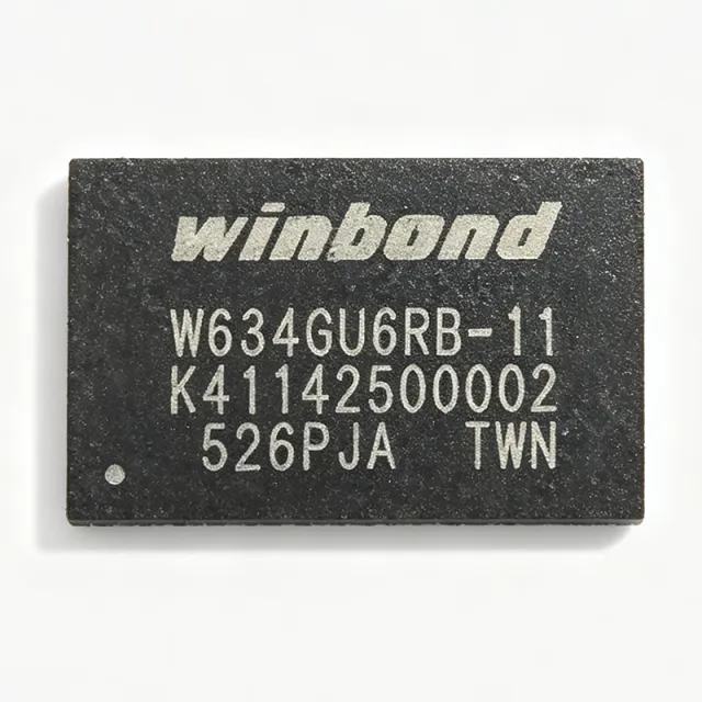
W634GU6RB-11 - 4Gb DDR3L SDRAM 933MHz | Winbond
W634GU6RB-11

W634GU6RB-11 - 4Gb DDR3L SDRAM 933MHz | Winbond

The W634GU6RB-11 is a 4Gbit DDR3L SDRAM memory IC from Winbond Electronics, organized as 256M x 16 bits. It operates at a clock frequency of 933 MHz (DDR3L-1866) with a CAS latency of 20 ns, and is supplied in a 96-ball VFBGA (7.5x13 mm) package. This device is designed for low-power applications, operating from a 1.35V supply (1.283V to 1.45V range), and supports parallel interface with a data rate of 1866 MT/s. DDR3L (Double Data Rate 3 Low Voltage) SDRAM is a type of synchronous dynamic random-access memory that transfers data on both edges of the clock signal, effectively doubling the data rate. It is a low-voltage variant of DDR3, operating at 1.35V instead of the standard 1.5V, reducing power consumption by about 20% compared to standard DDR3. DDR3L is part of the DDR SDRAM family, which includes DDR, DDR2, DDR3, and DDR4, and is widely used in computing, networking, and embedded systems where high bandwidth and low power are critical. Key features of the W634GU6RB-11 include auto self-refresh, auto precharge, data mask, write leveling, ZQ calibration, asynchronous reset, and dynamic on-chip termination (ODT). These features enhance signal integrity and simplify system design. The device supports a temperature range of -40°C to +95°C, making it suitable for industrial applications. It is RoHS compliant and halogen-free, aligning with environmental standards. Technically, the W634GU6RB-11 utilizes a 96-ball VFBGA package with a 7.5x13 mm footprint, offering a compact solution for space-constrained designs. The 20 ns CAS latency ensures fast access times, while the 933 MHz clock speed provides high bandwidth for data-intensive tasks. The device includes on-die termination (ODT) to improve signal quality on the memory bus, and supports write leveling for improved timing margins in multi-rank configurations. Typical applications include networking equipment (routers, switches), industrial computing, embedded systems, and consumer electronics such as set-top boxes and smart TVs. Its low voltage and high density make it ideal for power-sensitive designs where performance and efficiency are balanced. When designing with this device, ensure proper decoupling capacitors are placed near the VDD and VDDQ pins to minimize noise. Also, follow the JEDEC DDR3L layout guidelines for signal integrity, especially for high-speed signals. The device supports a 1.35V supply, so verify that the power management IC provides a stable 1.35V rail.

USD $13,52 Contacto
W634GU6RB-11TR - 4Gb DDR3L SDRAM 933MHz | Winbond
W634GU6RB-11TR

W634GU6RB-11TR - 4Gb DDR3L SDRAM 933MHz | Winbond

The W634GU6RB-11TR is a 4Gbit DDR3L SDRAM memory IC from Winbond Electronics, organized as 256M x 16 bits. It operates at a clock frequency of 933 MHz (DDR3L-1866) with a CAS latency of 13, and features a parallel interface with a 20 ns access time. The device is housed in a compact 96-ball VFBGA (7.5x13 mm) package, making it suitable for space-constrained applications requiring high memory density. DDR3L (Double Data Rate 3 Low Voltage) SDRAM is a type of synchronous dynamic random-access memory that operates at a lower voltage (1.35V) compared to standard DDR3 (1.5V), reducing power consumption by up to 20% while maintaining similar performance. It is part of the memory hierarchy in computing systems, serving as the main working memory for processors, and is widely used in laptops, embedded systems, networking equipment, and industrial applications. Key features of the W634GU6RB-11TR include support for 1.35V operation (with 1.5V compatibility), auto self-refresh, auto precharge, data mask, write leveling, ZQ calibration, asynchronous reset, and dynamic on-chip termination (ODT). These features enhance signal integrity and simplify system design. The device is RoHS compliant and halogen-free, meeting environmental standards. Technically, the W634GU6RB-11TR uses a 96-ball VFBGA package with a 0.8mm ball pitch, providing excellent thermal and electrical performance. The 933 MHz clock rate enables data rates up to 1866 MT/s, delivering high bandwidth for demanding applications. The device supports a temperature range of -40°C to +95°C, making it suitable for industrial environments. Typical applications include embedded computing, networking routers and switches, industrial automation, and high-performance consumer electronics. Its low voltage and high density make it ideal for power-sensitive designs. When designing with this memory, ensure proper decoupling capacitors near the VDD and VDDQ pins, and follow the PCB layout guidelines in the datasheet to minimize signal integrity issues at high speeds.

Cotización Contacto
W634GU6RB-12 - 4Gb DDR3L SDRAM x16 933MHz | Winbond
W634GU6RB-12

W634GU6RB-12 - 4Gb DDR3L SDRAM x16 933MHz | Winbond

The W634GU6RB-12 is a 4Gbit DDR3L SDRAM from Winbond Electronics, organized as 256M x 16, operating at 1.35V with a parallel interface. It is housed in a 96-ball VFBGA (7.5x13mm) package and supports DDR3L-1600 (11-11-11) speed grade at 933 MHz clock. This memory IC is designed for high-bandwidth applications requiring low power consumption and high reliability. DDR3L SDRAM is a type of double data rate synchronous dynamic random-access memory that operates at a lower voltage (1.35V) compared to standard DDR3 (1.5V), reducing power consumption by up to 20% while maintaining similar performance. It is part of the DDR3 memory family, which uses 8n-prefetch architecture and on-die termination to achieve high data rates. DDR3L is widely used in mobile, embedded, and industrial systems where power efficiency is critical. Key features include a 4Gbit density, x16 organization, 933 MHz clock speed (DDR3L-1600), 20 ns tRCD, and a 96-ball VFBGA package. The device supports industrial temperature grades: the -12I grade guarantees -40°C to 95°C case temperature, and the -12J grade guarantees -40°C to 105°C. It is RoHS compliant and halogen-free, meeting environmental standards. The W634GU6RB-12 utilizes advanced DRAM process technology, offering high-speed data transfer with low power consumption. The 8n-prefetch architecture enables burst lengths of 8, and the on-die termination (ODT) improves signal integrity. The device includes programmable CAS latency, burst length, and output drive strength, providing flexibility for system optimization. Typical applications include networking equipment, industrial automation, embedded computing, and consumer electronics such as set-top boxes and smart TVs. The low voltage and high density make it ideal for space-constrained designs requiring large memory capacity. When designing with this device, ensure proper decoupling capacitors near the VDD and VDDQ pins, and follow the PCB layout guidelines in the datasheet to minimize signal integrity issues. The device requires a 1.35V supply and a separate VDDQ supply, which should be well-regulated.

Cotización Contacto
W634GU6RB09I - 4Gb DDR3L SDRAM x16 1066MHz | Winbond
W634GU6RB09I

W634GU6RB09I - 4Gb DDR3L SDRAM x16 1066MHz | Winbond

The W634GU6RB09I is a 4Gbit DDR3L SDRAM memory IC from Winbond Electronics, organized as 256M x 16 bits. It operates at a clock frequency of 1.067 GHz (DDR3L-2133) with a CAS latency of 20 ns, and is housed in a 96-ball VFBGA (7.5x13 mm) package. This device is designed for low-voltage operation at 1.35V, making it suitable for power-sensitive applications such as mobile devices, embedded systems, and networking equipment. DDR3L (Double Data Rate 3 Low Voltage) is a type of synchronous dynamic random-access memory (SDRAM) that operates at 1.35V, reducing power consumption by about 20% compared to standard DDR3 (1.5V). It is part of the DDR3 family, which uses double data rate signaling to transfer data on both edges of the clock, achieving high bandwidth. DDR3L is widely used in laptops, servers, and industrial applications where energy efficiency is critical. Key features include a 4Gbit density, x16 data bus width, 1.067 GHz maximum clock speed, and industrial temperature range (-40°C to +95°C). The device supports burst lengths of 8 and 4, on-die termination (ODT), and programmable CAS latency. It is RoHS compliant and lead-free, meeting environmental standards. Technically, the W634GU6RB09I uses a 96-ball VFBGA package with a 0.8mm ball pitch, enabling high-density mounting on PCBs. The memory core is based on advanced DRAM process technology, providing high reliability and performance. The device includes auto-refresh and self-refresh modes for low-power standby, and supports DLL (Delay-Locked Loop) for precise timing. Typical applications include embedded computing, networking routers, industrial automation, and consumer electronics such as set-top boxes and smart TVs. Its low voltage and high density make it ideal for designs requiring large memory capacity with minimal power draw. When designing with this component, ensure proper decoupling capacitors near the power pins and follow the layout guidelines in the datasheet to minimize signal integrity issues. The device requires a 1.35V supply and a separate VDDQ for I/O, which should be regulated accurately.

Cotización Contacto
W634GU6RB09J - 4Gb DDR3L SDRAM x16 1066MHz | Winbond
W634GU6RB09J

W634GU6RB09J - 4Gb DDR3L SDRAM x16 1066MHz | Winbond

The Winbond W634GU6RB09J is a 4Gbit DDR3L SDRAM organized as 256M x 16, operating at 1.35V with a data rate of 1066MHz (DDR3L-2133). It comes in a 96-ball VFBGA (7.5x13mm) package, offering a compact footprint for space-constrained designs. This memory IC is designed for high-bandwidth applications requiring low power consumption, making it ideal for mobile, embedded, and networking systems. DDR3L (Double Data Rate 3 Low Voltage) is a type of synchronous dynamic random-access memory (SDRAM) that operates at 1.35V, reducing power consumption by about 20% compared to standard 1.5V DDR3. It is part of the DDR3 family, which uses double data rate signaling to transfer data on both edges of the clock, achieving high throughput. DDR3L is backward-compatible with DDR3 and is widely used in laptops, servers, and industrial electronics where energy efficiency is critical. Key features include a 4Gbit density, x16 organization, 1.067 GHz clock speed, and a CAS latency of 20 ns. The device supports on-die termination (ODT), programmable CAS latency, and burst lengths of 8 and 4. It operates over a temperature range of 0°C to +95°C (case temperature) and is RoHS compliant. The 96-VFBGA package measures 7.5x13mm with a 0.8mm ball pitch, enabling high-density PCB layouts. Technically, the W634GU6RB09J uses a 30nm-class process technology, achieving low power and high speed. It features internal calibration for ZQ, write leveling, and read leveling to ensure signal integrity at high frequencies. The device supports auto-refresh and self-refresh modes, reducing standby power. Its low voltage operation and advanced power management make it suitable for battery-powered devices. Typical applications include mobile computing, networking equipment, industrial automation, and consumer electronics such as set-top boxes and smart TVs. The high density and low power make it ideal for systems requiring large memory capacity with minimal energy consumption. When designing with this component, ensure proper decoupling capacitors near the power pins and follow the layout guidelines in the datasheet to maintain signal integrity at 1066MHz. The device requires a 1.35V supply and a separate VDDQ, which should be regulated accurately.

Cotización Contacto
W634GU6RB11I - 4Gb DDR3L SDRAM x16 933MHz | Winbond
W634GU6RB11I

W634GU6RB11I - 4Gb DDR3L SDRAM x16 933MHz | Winbond

The W634GU6RB11I is a 4Gbit DDR3L SDRAM memory IC from Winbond Electronics, organized as 256M x 16 bits. It operates at a clock frequency of 933 MHz (DDR3L-1866) with a CAS latency of 20 ns, and is supplied in a 96-ball VFBGA package measuring 7.5 x 13 mm. This device is designed for low-voltage operation at 1.35V, reducing power consumption by approximately 15% compared to standard 1.5V DDR3, making it ideal for power-sensitive applications. DDR3L SDRAM (Double Data Rate 3 Low Voltage) is a type of synchronous dynamic random-access memory that transfers data on both edges of the clock signal, effectively doubling the data rate. It operates at a lower voltage (1.35V) than standard DDR3 (1.5V), offering improved energy efficiency. DDR3L is part of the DDR SDRAM family, which includes DDR, DDR2, DDR3, and DDR4, and is widely used in computing, networking, and embedded systems where high bandwidth and low power are critical. Key features of the W634GU6RB11I include a parallel interface with a 16-bit data bus, support for industrial temperature range (-40°C to +95°C), and compatibility with JEDEC DDR3L standards. The device offers burst lengths of 8 and 4, on-die termination (ODT), and programmable CAS latency. Its low-voltage operation and high density make it suitable for applications requiring large memory capacity with minimal power draw. The W634GU6RB11I utilizes advanced DRAM process technology, achieving high-speed data transfer while maintaining low power consumption. The 96-ball VFBGA package provides excellent thermal and electrical performance, with a compact footprint suitable for space-constrained designs. The device supports auto-refresh and self-refresh modes, ensuring data integrity with minimal power consumption during idle periods. Typical applications include networking equipment (routers, switches), industrial automation, embedded computing, and consumer electronics such as set-top boxes and smart TVs. Its industrial temperature rating makes it suitable for harsh environments, while the low-voltage operation extends battery life in portable devices. When designing with this component, ensure proper decoupling capacitors are placed near the power pins to minimize noise. The VFBGA package requires careful PCB layout to route the fine-pitch balls, and the DDR3L interface should be terminated according to JEDEC guidelines to maintain signal integrity.

Cotización Contacto
W634GU6RB11J - 4Gb DDR3L SDRAM x16 933MHz | Winbond
W634GU6RB11J

W634GU6RB11J - 4Gb DDR3L SDRAM x16 933MHz | Winbond

The Winbond W634GU6RB11J is a 4Gbit DDR3L SDRAM organized as 256M x 16, operating at a clock frequency of 933 MHz (DDR3L-1866) with a data rate of 1866 MT/s. It is housed in a 96-ball VFBGA package (7.5x13 mm) and operates from a 1.35V supply, making it suitable for low-power applications. The device supports parallel interface with a burst length of 8 and features a 20 ns CAS latency. DDR3L (Double Data Rate 3 Low Voltage) is a type of synchronous dynamic random-access memory (SDRAM) that operates at 1.35V, reducing power consumption by about 20% compared to standard DDR3 (1.5V). It is part of the DDR3 family, which uses double data rate signaling to transfer data on both edges of the clock, achieving high bandwidth. DDR3L is commonly used in mobile devices, embedded systems, and industrial applications where power efficiency is critical. Key features include auto self-refresh, auto precharge, data mask, write leveling, ZQ calibration, asynchronous reset, and dynamic on-chip termination (DTC). These features enhance signal integrity and simplify system design. The device supports industrial temperature range from -40°C to +95°C, making it suitable for harsh environments. It is RoHS compliant and halogen-free, aligning with environmental standards. Technically, the W634GU6RB11J uses a 96-ball VFBGA package with a 0.8mm ball pitch, providing excellent thermal and electrical performance. The memory array is organized in 8 banks, and the device supports programmable CAS latency (CL) and additive latency (AL) for flexible timing. The on-die termination (ODT) feature improves signal quality by matching impedance, reducing reflections on the data bus. Typical applications include networking equipment, industrial automation, medical devices, and embedded computing systems where high-density, low-power memory is required. The 4Gb density and x16 organization make it ideal for applications needing moderate memory capacity with a wide data bus. When designing with this device, ensure proper decoupling capacitors near the VDD and VDDQ pins to minimize power supply noise. Also, follow the JEDEC DDR3L layout guidelines for signal integrity, including controlled impedance traces and proper termination.

Cotización Contacto
W634GU6RB12I - 4Gb DDR3L SDRAM x16 800MHz | Winbond
W634GU6RB12I

W634GU6RB12I - 4Gb DDR3L SDRAM x16 800MHz | Winbond

The W634GU6RB12I is a 4Gbit DDR3L SDRAM organized as 256M x 16, operating at 1.35V with a data rate of 800MHz (DDR3L-1600). It is housed in a 96-ball VFBGA (7.5x13mm) package and is designed for industrial temperature range (-40°C to +95°C). This memory IC is ideal for applications requiring high-density, low-power volatile storage. DDR3L (Double Data Rate 3 Low Voltage) is a type of synchronous dynamic random-access memory (SDRAM) that operates at 1.35V, reducing power consumption by about 20% compared to standard DDR3 (1.5V). It is part of the DDR3 family, which uses double data rate signaling to transfer data on both edges of the clock, achieving high bandwidth. DDR3L is commonly used in computing, networking, and embedded systems where power efficiency is critical. Key features include a parallel interface with 800MHz clock speed, 20ns row cycle time, and support for industrial temperature grades. The device is RoHS compliant and halogen-free, meeting environmental standards. The 96-ball VFBGA package offers a compact footprint suitable for space-constrained designs. The W634GU6RB12I utilizes advanced DRAM process technology, providing reliable performance with low power consumption. It supports standard DDR3L features such as on-die termination (ODT), programmable CAS latency, and burst lengths of 8. The industrial temperature grade ensures operation in harsh environments. Typical applications include industrial automation, networking equipment, embedded computing, and automotive infotainment systems. Its high density and low power make it suitable for memory-intensive tasks in these domains. When designing with this device, ensure proper decoupling and signal integrity practices are followed, as high-speed memory interfaces require careful PCB layout to minimize noise and reflections.

Cotización Contacto
W634GU6RB12J - 4Gb DDR3L SDRAM 933MHz | Winbond
W634GU6RB12J

W634GU6RB12J - 4Gb DDR3L SDRAM 933MHz | Winbond

The W634GU6RB12J is a 4Gbit DDR3L SDRAM from Winbond Electronics, organized as 256M x 16 and operating at 1.35V. It features a parallel interface with a clock speed of 933 MHz (DDR3L-1866) and a CAS latency of 20 ns. The device is housed in a 96-ball VFBGA package (7.5x13 mm) and is designed for high-bandwidth memory applications. DDR3L SDRAM is a type of dynamic random-access memory that operates at a lower voltage (1.35V) compared to standard DDR3 (1.5V), reducing power consumption while maintaining high data rates. It is part of the DDR3L memory family, which is widely used in computing, networking, and industrial applications where power efficiency is critical. Key features include a 4Gbit density, x16 organization, 933 MHz clock speed, and support for the DDR3L-1866 specification. The device offers a burst length of 8 and supports on-die termination (ODT) for improved signal integrity. It operates over a temperature range of -40°C to +105°C (TCASE) for the 12J industrial plus grade, making it suitable for harsh environments. The W634GU6RB12J utilizes advanced DRAM process technology to achieve high speed and low power. It includes features such as programmable CAS latency, write leveling, and self-refresh modes to optimize performance and power consumption. The 96-ball VFBGA package provides excellent thermal and electrical performance. Typical applications include embedded systems, networking equipment, industrial automation, and automotive infotainment. The low voltage and high speed make it ideal for power-sensitive designs that require high memory bandwidth. When designing with this device, ensure proper decoupling and signal integrity practices are followed. The DDR3L interface requires careful PCB layout to minimize crosstalk and maintain signal quality at high speeds.

Cotización Contacto
W681308DG - USB Audio Controller 16-bit 48-LQFP | Nuvoton
W681308DG

W681308DG - USB Audio Controller 16-bit 48-LQFP | Nuvoton

The Nuvoton W681308DG is a USB audio controller IC with an integrated 16-bit audio codec, housed in a 48-pin LQFP (7x7 mm) surface-mount package. As a member of the Winbond/Nuvoton W6813 series of USB audio controllers, it integrates a USB controller, audio codec, and embedded microcontroller into a single chip for USB audio peripheral designs. A USB audio controller is a mixed-signal device that implements the USB audio class protocol on the digital side and an audio codec (codec = coder-decoder) on the analog side. Within the system hierarchy, it sits between a general-purpose USB microcontroller and a dedicated audio codec: it handles USB enumeration, audio streaming, clocking, and sample-rate conversion, while also providing microphone and speaker signal paths. This integration reduces bill-of-materials count compared to a discrete USB MCU plus external codec solution. Key features of the W681308DG include a 16-bit audio data path, USB full-speed audio transport, integrated microphone and speaker audio channels, and a compact 7x7 mm 48-LQFP footprint that supports consumer peripheral form factors. The device operates from a 3.3 V supply, consistent with the family datasheet description of the W681308 series as a 3.3 V part. Architecturally, the W681308 combines an 8-bit CISC microcontroller core with on-chip program memory and a hardwired USB audio function block. The codec front end handles anti-aliasing filtering, ADC for microphone inputs, and DAC for speaker outputs, while the MCU firmware manages HID interfaces, mute/volume controls, and other USB descriptor behavior. Refer to the manufacturer datasheet for precise clock, PLL, and interface specifications. Typical applications include USB headset and headphone amplifiers, desktop microphone arrays, USB speakerphones, VoIP handsets, and general USB audio dongles where a single-chip, low-cost USB audio solution is required. A key design consideration is analog layout: the microphone preamp and DAC outputs are sensitive to digital return-path noise, so a solid ground plane, careful separation of analog and digital traces, and proper decoupling of the 3.3 V rail per the manufacturer datasheet recommendations are essential for a low-noise result. This page synthesizes distributor sourcing data, datasheet references, and practical design notes not found in the manufacturer datasheet.

Cotización Contacto
W77C032A40FL - 40MHz 8-Bit ROMless MCU | Nuvoton
W77C032A40FL

W77C032A40FL - 40MHz 8-Bit ROMless MCU | Nuvoton

The Nuvoton W77C032A40FL is a ROMless Turbo-51 8-bit microcontroller operating at up to 40 MHz, with 1K x 8 bits of RAM, 36 I/O pins, and a 44-pin BQFP package. Designed for embedded control applications, the device combines a high-clock-speed 8051-compatible core with an internal oscillator, allowing designers to build compact control systems without adding an external program-memory device. An 8-bit microcontroller is a semiconductor integrated circuit containing a central processing unit, memory, I/O ports, and peripheral functions on one package. In the product hierarchy, it belongs to the microcontroller family of embedded processors and embedded ICs. The W77C032A40FL belongs to the Turbo-51 family and uses a ROMless architecture, meaning program storage must be supplied by external memory while working data can be held in its internal RAM. Key characteristics include a maximum clock frequency of 40 MHz, 1K x 8-bit SRAM, and 36 general-purpose I/O lines. Its internal oscillator reduces the external clock-component count, while the 44-BQFP package exposes substantially more I/O than smaller dual-inline or small-outline packages. These characteristics make the MCU appropriate for compact controllers with multiple discrete inputs and outputs, particularly where an 8051-compatible instruction set and external program memory are required. The W77C032A40FL is positioned as a ROMless Turbo-51 device rather than a self-contained MCU with embedded Flash. External program memory and interface circuitry therefore influence the complete memory system. Its 36 I/O pins provide ample connectivity for control signals, indicators, relays, sensors, and communication peripherals. Because the device is specified at 40 MHz, firmware timing, memory-access delays, peripheral clock requirements, and external-memory interface timing must be reviewed together during schematic and PCB design. Typical applications include industrial machine controls, building-control modules, appliance controllers, interface modules, and other embedded automation products. The combination of 36 I/O, internal RAM, and external program-memory support is especially useful when a product needs substantial I/O breadth but limited on-chip volatile memory. The MCU can act as the supervisory controller between sensors, actuators, communications circuitry, and discrete logic. A key design consideration is that ROMless operation requires careful implementation of the external memory interface and correct timing for the selected memory device. Place decoupling close to the supply pins, route oscillator and memory signals consistently, and keep high-current switching nodes away from sensitive control inputs. Confirm pin multiplexing, reset behavior, and peripheral availability against the manufacturer datasheet before finalizing firmware and board connections. This page consolidates the principal electrical, memory, package, sourcing, and replacement information for W77C032A40FL. It also provides practical application guidance and design checks that help engineers determine whether this ROMless Turbo-51 MCU fits a control design before committing to PCB layout and external-memory implementation.

Cotización Contacto
W77C032A40PL - 40MHz ROMless 8051 MCU | Nuvoton
W77C032A40PL

W77C032A40PL - 40MHz ROMless 8051 MCU | Nuvoton

The Nuvoton Technology Corporation W77C032A40PL is an 8-bit ROMless 8051-compatible microcontroller operating at up to 40 MHz, with 1 KB x 8 RAM, 36 I/O lines, and a 44-pin PLCC package. The device uses the W77C032 Turbo-51 processor architecture, which reduces wasted instruction cycles and executes 8051 instructions approximately 1.5 to 3 times faster than a traditional 8051 core at the same clock speed. A microcontroller is a programmable semiconductor integrating a processor core, memory, I/O ports, timers, serial communications, and interrupt functions on one integrated circuit. The W77C032 belongs to the 8-bit MCU hierarchy and retains 8052 pin and instruction-set compatibility. Because the part is ROMless, application firmware must be supplied through external program-memory hardware, making the device suitable for systems that require flexible code storage, boot loading, field updating, or shared memory among several devices. The principal specifications include a 40 MHz maximum operating speed, 1 KB x 8 internal RAM, four 8-bit I/O ports, 36 total I/O lines, and an internal oscillator. The W77C032 also incorporates standard 8052 resources, including three 16-bit timer/counters, a full-duplex serial port, and multiple interrupt sources. Its 4.5 V to 5.5 V operating range and 44-PLCC package support established 5 V embedded-control architectures where a leaded, socket-compatible footprint is preferable to a fine-pitch surface-mount package. The redesigned processor core avoids wasted clock and memory cycles, improving execution efficiency without changing the familiar 8051 instruction set. This combination is useful when maintaining legacy 8051 source code while increasing control-loop or peripheral-handling performance. Since the MCU has no on-chip program memory, a system designer must account for external ROM or another memory source when creating the memory map, boot sequence, and firmware-loading architecture. Typical uses include industrial controllers, embedded data-acquisition equipment, communications controllers, legacy 8051 peripheral upgrades, and compact automation modules. The 36 I/O lines provide substantial parallel-interface capacity, while the timers and serial port reduce the need for external peripheral chips. Board-level designs should also provide a stable clock or oscillator arrangement, external program-memory interfacing, suitable decoupling, and adequate pin-compatible routing. A key design consideration is that the PLCC package has 44 positions, but the verified product records do not provide a complete numbered pin description. Engineers should therefore assign the PCB footprint and nets directly from the pin table and package drawing in the manufacturer data sheet rather than inferring connections from generic 8051 diagrams. Confirm the external-memory interface, reset behavior, clock requirements, and available I/O before finalizing the board layout. This product summary consolidates the confirmed architecture, memory, clock, package, sourcing, and lifecycle information with engineering guidance for external-memory implementation, firmware compatibility, and PLCC layout. It also distinguishes directly documented characteristics from parameters that still require confirmation from the complete manufacturer data sheet.

Cotización Contacto
W77E058A40FL - 40MHz 8051 32KB Flash MCU | Nuvoton
W77E058A40FL

W77E058A40FL - 40MHz 8051 32KB Flash MCU | Nuvoton

Nuvoton Technology Corporation W77E058A40FL is an 8-bit CMOS W77-series microcontroller with 32 KB of embedded Flash memory, a 40 MHz operating frequency, and a 44-BQFP package. It uses a four-clock machine-cycle 8051-compatible architecture and operates from a 5 V supply, combining legacy MCS-51 software compatibility with substantially faster instruction execution than the original standard 80C51 family. An 8051-compatible microcontroller is an embedded processor designed around the MCS-51 instruction set and its associated register, interrupt, timer, serial-interface, and port architecture. The W77 series places that established software ecosystem within the broader hierarchy of embedded controllers, 8-bit microcontrollers, and general-purpose semiconductor devices. This makes it useful for control systems that benefit from established 8051 tools and code while requiring higher processing throughput and integrated Flash rather than an external program-memory device. The W77E058A40FL combines several headline characteristics: 8-bit processing, 40 MHz operation, and 32 KB of embedded Flash. Its four-clock machine-cycle design executes each machine cycle in a quarter of a full 40 MHz clock period. The device also provides four 8-bit I/O ports and follows the MCS-51 instruction set, allowing engineers to reuse familiar driver concepts and peripheral-control code while selecting a faster Flash-based implementation. Technically, the part belongs to the W77 family and is positioned as a compact, 5 V embedded controller. Its Flash memory consolidates program storage on the die, simplifying the hardware arrangement compared with an architecture that requires external program memory. Because the controller remains compatible with the MCS-51 instruction set, software migration from an appropriate 80C52-class design can be easier than moving to a different instruction set. Board compatibility still requires verification of pin functions, electrical limits, memory organization, and peripheral availability. Typical applications include industrial keypad and panel controllers, motor and relay-sequencing modules, compact instrumentation, appliance-control boards, and legacy 8051 peripheral upgrades. The 40 MHz execution rate can improve responsiveness in polling loops, protocol handling, and time-dependent control tasks, while the four 8-bit I/O ports support digital input, output, and external-interface connections when the remaining pins provide the required clock, reset, and power functions. A key design consideration is that pin-compatible software does not automatically prove drop-in electrical compatibility. Before replacing an existing 8051 device, verify the 44-BQFP footprint, pin assignments, reset behavior, operating voltage, oscillator connections, I/O drive limits, and peripheral functions against the current datasheet. Programming and development-tool requirements should also be checked because instruction-set compatibility does not guarantee that every legacy programmer supports the device. This product page combines the W77E058A40FL's core specifications, verified component listings, application guidance, design checks, and a transparent comparison of candidate cross-reference devices. It also distinguishes confirmed drop-in options from merely similar controllers, helping engineers make a replacement decision without relying on package similarity alone.

Cotización Contacto
W77E058A40PL - 40MHz 8051 MCU, 32KB Flash | Nuvoton
W77E058A40PL

W77E058A40PL - 40MHz 8051 MCU, 32KB Flash | Nuvoton

Nuvoton Technology Corporation W77E058A40PL is an 8-bit CMOS 8051-compatible microcontroller operating at up to 40 MHz, with 32KB of Flash memory in a 44-pin PLCC package. It executes four clocks per machine cycle, provides two UART devices and two DPTR registers, and operates from a 5 V supply across the 4.5 V to 5.5 V range. The W77E058A family is also pin-compatible with traditional 12T 8051 devices. An 8051 microcontroller is an embedded-computing IC that combines a CPU core, program memory, data memory, I/O ports, and peripherals on one integrated circuit. Within the product hierarchy, the W77E058A is an 8-bit MCU, a 4T 8051 MCU, a member of the MCS-51 instruction-set family, and a member of the broader embedded processor and semiconductor categories. Its 8051 compatibility supports established compiler, debugger, and application-development ecosystems. Key features include a 40 MHz maximum operating frequency, a four-clock machine-cycle architecture, and 32KB of on-chip Flash organized as 32K by 8 bits. Two UART devices support serial communication, while two DPTR registers provide separate 16-bit pointer contexts. Four 8-bit I/O ports support digital interfaces, and the 4.5 V to 5.5 V operating range aligns the device with conventional 5 V embedded equipment. The device uses an 8-bit CISC architecture compatible with the MCS-51 instruction set and remains compatible with traditional 12T 8051 interfaces. Its 4T architecture reduces the clock-to-machine-cycle ratio to four clocks, allowing 40 MHz operation without changing the fundamental software timing model. Because the product is identified as NRND, engineers should verify availability and consider the manufacturer's current portfolio before starting a new design. Typical applications include security and alarm systems, communication equipment, industrial control, power-management controllers, and industrial personal computers. The two UARTs are useful for sensor, transceiver, display, or host serial links, while the four parallel I/O ports can handle digital control signals, status indicators, relay logic, or keypad interfaces. The principal design consideration is the 5 V supply requirement and the limited 0°C to 70°C temperature range. Decoupling and signal-integrity practices remain important because all peripherals share the same supply and ground system. Engineers should also confirm the PLCC-44 footprint, pin assignments, and board-level clearances against the manufacturer datasheet before layout release. This page combines the manufacturer's family-level architecture and lifecycle information with distributor specifications and a practical replacement assessment. It also identifies the package, programming interface considerations, application fit, and design checks needed to evaluate the W77E058A40PL in an embedded control platform.

Cotización Contacto