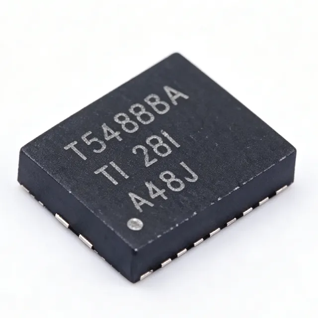
TPS548B28RWWR - 20A 16V Sync Buck Converter | TI | Datacenter
MPN: TPS548B28RWWR ✓ فعال| تعداد | قیمت واحد | قیمت کل |
|---|---|---|
| 1 | $1 | $1.00 |
TPS548B28RWWR نمای کلی
A synchronous buck converter is a DC-DC switching regulator that steps a higher input voltage down to a lower output voltage using two integrated switches (high-side and low-side MOSFETs) plus an external inductor. Within the power management hierarchy, the TPS548B28 belongs to the switching regulator family, positioned as a single-channel point-of-load (POL) solution between simple low-current bucks and multi-phase controllers.
Key features include a 4V to 16V input range supporting 20A continuous output without external bias, extended 2.7V operation with a 3.13V to 3.6V external bias, an output voltage range of 0.6V to 5.5V, and integrated 7.7-mΩ high-side and 2.4-mΩ low-side MOSFETs. The device offers fast load-transient response, accurate load and line regulation, Skip-mode or forced-CCM (FCCM) operation for light-load efficiency trade-offs, programmable soft start, and hiccup current limit for fault robustness.
The D-CAP3-style control architecture enables a small external component count and fast transient response with low output capacitance, well suited to space-constrained boards. The internal 3V LDO can be overridden by an external bias rail to improve efficiency at lower input voltages. Differential remote sense compensates for PCB IR drop, maintaining ±1% regulation at the load point.
Typical applications include server and storage point-of-load rails (DSP, FPGA, ASIC, and processor cores), datacenter and networking card power, and general industrial 20A-class low-voltage supplies. Reference design support is available via the TPS548B28EVM-023 evaluation module.
Design consideration: at 20A loads, minimize the SW-node copper area and optimize the input capacitor loop to control EMI; verify thermal performance since total MOSFET conduction plus switching losses concentrate in the small QFN footprint.
جایگزینهای drop-in برای TPS548B28RWWR — همان پکیج، سازگار پینبهپین. قطعات با پکیج متفاوت که نیاز به تغییر PCB دارند مستثنی هستند.
ابزار مقایسه سریع — قطعات جایگزین را برای مقایسه کنار به کنار انتخاب کنید:
هیچ جایگزین مستقیمی برای این محصول موجود نیست.
درخواست جایگزینTPS548B28RWWR حداکثر مقادیر مجاز و مشخصات الکتریکی
| توپولوژی | Synchronous Step-Down (Buck) Converter |
| Input Voltage Range (no external bias) | 4 V to 16 V |
| Input Voltage Range (with external bias) | 2.7 V to 16 V |
| External Bias Range | 3.13 V to 3.6 V |
| حداکثر جریان خروجی | 20 A |
| محدوده ولتاژ خروجی | 0.6 V to 5.5 V |
| ولتاژ مرجع | 0.6 V ±1% over junction temperature |
| High-Side MOSFET RDS(on) | 7.7 mΩ |
| Low-Side MOSFET RDS(on) | 2.4 mΩ |
| Remote Sense | Differential remote sense |
| Light Load Mode | Skip-mode or FCCM (selectable) |
| محدودیت جریان | Hiccup mode current limit |
| شروع نرم | Programmable |
| Internal LDO | 3 V internal LDO |
| بستهبندی | 21-PowerVFQFN (RWW) |
| نوع نصب | Surface Mount |
پیکربندی پین TPS548B28RWWR
| پین 20 | SW — Switch node - connects to output inductor; per TI E2E forum, SW sends PWM to the inductor which maintains steady output current |
| پین [DATA_NEEDED] | VIN — Input supply |
| پین [DATA_NEEDED] | GND — Ground |
| پین [DATA_NEEDED] | VOUT/SENSE — Differential remote sense inputs |
| پین [DATA_NEEDED] | BOOT — High-side gate drive bootstrap |
| پین [DATA_NEEDED] | EN — Enable |
| پین [DATA_NEEDED] | SS/VSEL — Soft start / mode configuration |
| پین [DATA_NEEDED] | BIAS/VDD — External bias input for internal LDO bypass |
کاربردهای معمول
TPS548B28RWWR مناسب است برای 3 کاربردs: مدیریت توان, کنترل موتور, روشنایی LED.
مدیریت توان
سوئیچینگ و تنظیم در مدارهای منبع تغذیه با استفاده از TPS548B28RWWR.
کنترل موتور
راهاندازی و کنترل موتورهای DC/BLDC با TPS548B28RWWR.
روشنایی LED
راهاندازی رشتهها و آرایههای LED با TPS548B28RWWR.
هیچ پرسش متداولی برای این محصول موجود نیست.
دادههای مرجع مهندسی برای TPS548B28RWWR — مقایسه، راهنمای طراحی و اطلاعات انطباق.
راهنمای انتخاب
تفاوتهای کلیدی
- Differential remote sense for ±1% load-point accuracy (در مقابلTPS53622RSBT)
- Integrated 7.7 mΩ / 2.4 mΩ MOSFETs (در مقابلTPS53355)
- Internal 3V LDO with external bias override (در مقابلTPS548B28EVM-023 reference configuration)
یادداشتهای طراحی
Keep the input capacitor to VIN/GND loop as small as possible; the 20A pulsed currents in this loop dominate EMI. Per the TI datasheet layout section, place ceramic input capacitors directly at the VIN pins and use the PowerVFQFN thermal pad with a multi-layer via array to the ground plane for heat spreading.
Conduction losses are roughly I^2 x (RDSon_HS x D + RDSon_LS x (1-D)); with 7.7 mΩ and 2.4 mΩ MOSFETs, duty cycle strongly affects thermals. At 12V-to-1V, 20A designs, evaluate switching loss and consider Skip-mode only at light load, since FCCM improves transient response for processor cores.
Do not attempt to parallel multiple TPS548B28 outputs - per TI E2E forum, the device does not support paralleling; for higher current use a controller such as TPS53355. The 4V minimum input applies without external bias; below 4V, supply a 3.13V-3.6V bias to extend operation down to 2.7V.
اطلاعات انطباق
Compliance data not present in provided verified web data; check TI product page for RoHS/REACH status.







