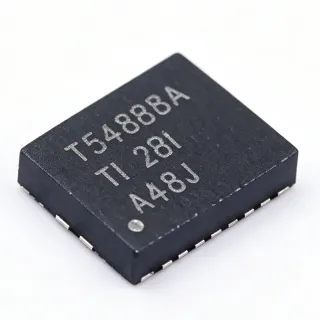
TPS548B28 - 20A, 16V Synchronous Buck Converter | TI
MPN: TPS548B28 ✓ Active| Qty | Unit Price | Extended |
|---|---|---|
| 1 | $6.15 | $6.15 |
| 10 | $5.53 | $55.30 |
| 100 | $4.78 | $478.00 |
| 500 | $4.12 | $2,060.00 |
| 1,000 | $3.72 | $3,720.00 |
TPS548B28 Overview
A synchronous buck converter (also called a step-down switching regulator) is a DC-DC power management IC that uses integrated high-side and low-side MOSFETs plus an external inductor to convert a higher input voltage to a lower output voltage with high efficiency. Within the power-management hierarchy, the TPS548B28 sits at the point-of-load (POL) regulator level of server, storage, and computing power trees.
Key features include 4-V to 16-V input range up to 20 A without external bias (2.7-V to 16-V with external bias from 3.13 V to 3.6 V), integrated 7.7-mΩ high-side and 2.4-mΩ low-side MOSFETs supporting 20-A continuous output, Skip-mode or FCCM operation for light-load efficiency, and programmable soft start. Differential remote sense improves output accuracy at the load point in dense boards.
Technically, the integrated power stage minimizes external component count, making the part well-suited to space-constrained datacenter applications. Fast load-transient response, accurate load and line regulation, and hiccup-mode overcurrent protection improve system robustness; the internal 3-V LDO simplifies bias by allowing operation directly from the input rail.
Typical applications include server and storage point-of-load rails, networking line cards, and computing ASIC/FPGA/DSP power supplies requiring 20 A or less at 0.6-V to 5.5-V outputs.
Design tip: use the TPS548B28EVM-023 evaluation board as a layout reference, keep the SW loop compact, and note the device is not intended for paralleled outputs - use TPS53355 or LM27403 for parallel designs.
Drop-in alternatives for TPS548B28 — same package, pin-to-pin compatible. Different-package parts requiring PCB rework are excluded.
Quick Comparison Tool — Select alternative parts for side-by-side comparison:
TPS548B22RWER
✅ Drop-In ⚠️ Specs Unverified📋 Reference alternative (not in catalog)
TPS549B22RWER
✅ Drop-In ⚠️ Specs Unverified📋 Reference alternative (not in catalog)
TPS548B28 Maximum Ratings & Electrical Characteristics
| Topology | Synchronous Buck Converter |
| Input Voltage Range (with external bias) | 2.7 V to 16 V |
| Input Voltage Range (no external bias) | 4 V to 16 V |
| External Bias Range | 3.13 V to 3.6 V |
| Output Voltage Range | 0.6 V to 5.5 V |
| Maximum Output Current | 20 A |
| Reference Voltage | 0.6 V, ±1% over full junction temperature range |
| High-Side MOSFET Rds(on) | 7.7 mOhm |
| Low-Side MOSFET Rds(on) | 2.4 mOhm |
| Light Load Mode | Skip-mode or FCCM selectable |
| Overcurrent Protection | Hiccup current limit |
| Soft-Start | Programmable |
| Remote Sense | Differential |
| Internal LDO | 3 V internal LDO |
| Package | 21-PowerVFQFN (RWW) |
| Mounting Type | Surface Mount |
TPS548B28 21-powervfqfn (rww) Pin Configuration Guide
Pin configuration for TPS548B28 (21-powervfqfn (rww) package). This power device features gate, drain, and source terminals. For non-polarized packages, refer to the manufacturer datasheet for exact pin 1 orientation and footprint details. Common applications include power supply design, motor driving, and load switching.

No detailed pinout data available for TPS548B28.
Refer to the datasheet for full pin configuration.
Typical Applications
TPS548B28 is suitable for 6 applications: Server Point-of-Load Power, Storage and SSD Systems, Networking and Telecom Line Cards, FPGA and DSP Core Power, Industrial Computing and Edge Systems, Optical Module and ASIC Accelerator Cards.
Server Point-of-Load Power
Server motherboards require tightly regulated low-voltage rails for ASICs, memory, and logic, often at 20 A or less. The TPS548B28 fits this role with its 20-A continuous rating, 0.6-V to 5.5-V adjustable output, and ±1% 0.6-V reference over the full junction temperature range. Its differential remote sense compensates for board IR drop so voltage is accurate at the load pin. With integrated 7.7-mOhm and 2.4-mOhm MOSFETs and a 3-V internal LDO, the external BOM shrinks, fitting the dense layouts typical of server POL design. Fast load-transient response handles step loads from bursty processors.
Recommended
Storage and SSD Systems
Enterprise storage controllers and SSD backplanes need efficient, compact 12-V-to-low-voltage conversion for NAND, controllers, and PHY rails. The TPS548B28 operates from a 4-V to 16-V input without external bias, directly accepting 12-V rails, and delivers up to 20 A with integrated MOSFETs. Skip-mode operation maintains efficiency at light load when storage is idle, while FCCM can be chosen to avoid mode-transient jitter. Hiccup current limit protects against shorted loads, and programmable soft start enables controlled power-up of storage subsystem rails in compliance with typical server startup sequencing requirements.
Recommended
Networking and Telecom Line Cards
Networking line cards distribute a 12-V or intermediate bus to many point-of-load regulators feeding ASICs, PHYs, and optical modules. The TPS548B28's 2.7-V to 16-V input range (with 3.13-V to 3.6-V external bias) covers both 12-V and intermediate-bus inputs. Accurate line and load regulation plus differential remote sense keep rails within tight windows despite card-level voltage drops. Its small footprint and few external components address the high POL density of switch line cards, and Skip-mode operation improves the light-load efficiency that dominates networking energy profiles under partial traffic.
Recommended
FPGA and DSP Core Power
FPGA and DSP core rails often demand sub-1-V outputs at several amps with tight accuracy and fast transient response. The TPS548B28 regulates down to 0.6 V with a ±1% reference over the full junction temperature range, meeting core-voltage accuracy requirements, and its fast load-transient response handles sudden clock-domain load steps during device configuration and operation. The 20-A rating covers mid-size FPGA core loads. Designers should follow the TI EVM-023 layout for compact SW loops to minimize switching transients and ensure stable D-CAP control behavior with low-ESR ceramic output capacitors.
Recommended
Industrial Computing and Edge Systems
Industrial PCs, edge gateways, and embedded controllers run from 12-V or 24-V-adjacent rails and need robust, protected POL conversion. The TPS548B28's hiccup current limit survives sustained short circuits on loads and recovers automatically, improving field reliability. The 4-V to 16-V no-bias input range accepts 12-V industrial rails directly using the internal 3-V LDO, reducing component count in compact enclosures. Its high efficiency from integrated 7.7-mOhm and 2.4-mOhm MOSFETs limits heat dissipation in sealed housings, and programmable soft start coordinates staged power-up of embedded processors and peripherals.
Recommended
Optical Module and ASIC Accelerator Cards
Accelerator cards and optical modules use dense 12-V-to-0.8-V/1.8-V rails with strict height and area limits. The TPS548B28's integrated power stage and minimal external parts reduce solution height and footprint versus discrete designs, while the 20-A capability feeds ASIC or transceiver rails directly. FCCM operation avoids light-load frequency variation that could interact with sensitive analog circuitry on optical front ends, and Skip-mode is selectable for purely digital rails. Designers should place input decoupling close to the VIN pins and reference the TI EVM-023 for validated component selection and layout.
Recommended
Recommended Products Summary
Engineering reference data for TPS548B28 — comparison, design guidance, and compliance information.
Selection Guide
Comparison with Alternatives
| Parameter | This Product | TPS548B22RWER | TPS549B22RWER | TPS53355 |
|---|---|---|---|---|
| Brand | Texas Instruments | Texas Instruments | Texas Instruments | Texas Instruments |
| Output Current | 20 A | ~30 A | ~20-30 A (family variant) | 30 A |
| Input Voltage Range | 2.7 V to 16 V (4-16 V no bias) | 2.7 V to 16 V | 2.7 V to 16 V (family variant) | Split rail: 4.5-13.2 V power stage |
| Output Voltage Range | 0.6 V to 5.5 V | 0.6 V to 5.5 V (family) | 0.6 V to 5.5 V (family) | 0.75 V to 2.775 V |
Key Differentiators
- Differential remote sense for load-point accuracy (vs TPS548B22RWER)
- No external bias needed from 4-V input (vs TPS53355)
- Integrated MOSFET simplicity vs controller designs (vs LM27403)
Design Notes
Follow the TPS548B28EVM-023 evaluation board layout as the reference design. Keep the high-frequency SW input loop (VIN decoupling capacitors to PGND) as compact as possible to minimize switching-radiated EMI. Place the output inductor and output capacitors close to the SW and VOUT pins, and route the differential remote sense lines as a paired trace away from SW and bootstrap nodes to preserve the ±1% output accuracy at the load.
For 4-V to 16-V inputs, the internal 3-V LDO powers the device directly - no external bias required. For inputs below 4 V, supply an external bias of 3.13 V to 3.6 V. Verify total power dissipation with the integrated 7.7-mOhm high-side and 2.4-mOhm low-side MOSFETs at your load current and ambient temperature; use the exposed pad with a solid ground plane array of thermal vias to conduct heat.
Do not connect TPS548B28 units in parallel for higher current - TI E2E engineers recommend TPS53355 or LM27403 for paralleled-output solutions. Also note that the SW pin (pin 20) switches PWM into the inductor and does not directly carry the 20-A DC output; sizing conductors only at SW misunderstands the current path, which flows through the inductor to the output capacitors.
Compliance Information
Compliance details not present in the verified web data; consult the TI product page environmental information for TPS548B28RWWR.