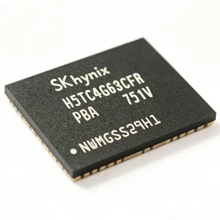
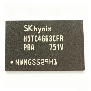
H5CG34MEBDX030N - DDR5 16Gb SDRAM Component | SK hynix | Server Memory
MPN: H5CG34MEBDX030N ✓ פעילH5CG34MEBDX030N סקירה
A DDR5 SDRAM is the fifth generation of the Double Data Rate synchronous DRAM standard defined by JEDEC. Unlike DDR4, DDR5 splits each rank into two independent 32-bit (or 40-bit with ECC) sub-channels per component/module, doubling effective channel concurrency and improving efficiency for multi-core server CPUs. In the memory hierarchy, the H5CG34MEBDX030N sits at the component level: DRAM die -> memory component -> memory module (RDIMM/LRDIMM/UDIMM) -> main-memory subsystem of a server or workstation.
Key features of the H5CG3 series include the reduced 1.1V core I/O supply (approximately 23% lower operating voltage than DDR4's 1.2V), on-die ECC (ODECC) that corrects single-bit internal errors without host overhead, decision-feedback equalization (DFE) on the data receiver path, and the DDR5 sub-channel architecture that enables two independent half-width channels per module. On-die termination (ODT), CA training, and same-bank refresh management further improve signal integrity and bandwidth utilization at high data rates.
Technically, the device uses a 16N/32N bank-group architecture with 16 banks across bank groups, and implements the DDR5 command/address encoding with dedicated VDDQ/VDD supplies (1.1V domains) plus a separate VPP 1.8V wordline boost supply for improved cell reliability. These features make it suitable for data-center RDIMM designs, AI and big-data compute nodes, and enterprise storage controllers.
Typical applications include server main memory modules (RDIMM/LRDIMM for 2DPC configurations), cloud and AI accelerator host memory, and high-performance workstations requiring high-capacity DDR5 ECC-class memory.
When designing with DDR5 components, ensure the PCB trace topology follows the DDR5 fly-by command/address routing and match data-line lengths within controller-specified skew; SPD configuration must reflect the exact die revision and DRAM configuration for reliable JEDEC-standard initialization.
This page synthesizes verified web data, drop-in alternatives from the same SK hynix DDR5 family, and engineering design notes not found on distributor listings. Full electrical timings should be confirmed against the official SK hynix DDR5 component datasheet before design release.
חלופות תחליף ישיר עבור H5CG34MEBDX030N — אותו מארז, תואם פין-לפין. חלקים במארז שונה הדורשים עיבוד מחדש של ה-PCB אינם נכללים.
וריאנטים בסדרה זו
דגמים מאותה סדרה התואמים Drop-in עם H5CG34MEBDX030N (אותו גורם צורה וטביעת רגל) — שונים ב Organization, Package, Density, Data Rate, Interface.
H5CG34MEBDX030
✅ Drop-Inצור קשר לקבלת מחיר
הצג גיליון נתונים ←H5CG44MEBDX014N
✅ Drop-Inצור קשר לקבלת מחיר
הצג גיליון נתונים ←H5CG46MEBDX015N
✅ Drop-Inצור קשר לקבלת מחיר
הצג גיליון נתונים ←H5CG48MEBDX014N
✅ Drop-Inצור קשר לקבלת מחיר
הצג גיליון נתונים ←H5CG44AGBDX018N
✅ Drop-Inצור קשר לקבלת מחיר
הצג גיליון נתונים ←H5CG34MEBDX030N דירוגים מרביים ומאפיינים חשמליים
| Manufacturer | SK hynix |
| Product Type | DDR5 SDRAM Component |
| Density | 16 Gbit (2 GB) |
| Memory Series | H5CG3 series (B-die) |
| DRAM Process Node | 1b-nanometer-class |
| Supply Voltage VDD/VDDQ | 1.1 V |
| Wordline Boost Supply VPP | 1.8 V |
| ממשק | DDR5 (JEDEC double data rate 5) |
| On-Die ECC | Yes (DDR5 ODECC) |
| Sub-Channel Architecture | Dual independent 32/40-bit sub-channels |
| Package Type | FBGA surface mount |
| ECC Feature | On-die ECC, no host overhead |
| Typical Application | Server RDIMM / LRDIMM components |
מדריך תצורת פינים של H5CG34MEBDX030N fbga surface mount
תצורת פינים עבור H5CG34MEBDX030N (מארזת fbga surface mount). מעגל משולב דיגיטלי זה כולל GPIO, ממשקי תקשורת (UART, SPI, I2C) ופיני מתח. יש לעיין בגיליון הנתונים של היצרן לפונקציות פינים חלופיות ולאפשרויות תצורה. חיוני לתכנון מערכות משובצות ולפריסת PCB.

אין נתוני פריסת פינים מפורטים עבור H5CG34MEBDX030N.
עיינו ב- גיליון נתונים עבור תצורת פינים מלאה.
יישומים טיפוסיים
H5CG34MEBDX030N מתאים עבור 6 יישוםs: Server RDIMM Main Memory, AI and Big-Data Compute Nodes, Enterprise Storage Controllers, Cloud Hypervisor Memory, High-Performance Workstations, Networking and Telecom Equipment.
Server RDIMM Main Memory
The H5CG34MEBDX030N serves as the core DRAM component on DDR5 registered DIMMs for 1U/2U servers. Its 16Gbit density allows 64GB+ RDIMMs from 32 ICs in dual-rank layouts, while the 1.1V supply cuts memory subsystem power versus DDR4. The on-die ECC corrects internal single-bit errors without host RAS overhead, and the dual 32-bit sub-channels let a server CPU address two independent half-width channels per module, improving queue depth and effective bandwidth for virtualized workloads. Designers should follow DDR5 fly-by CA routing and pair the DRAM with a registered clock driver, SPD hub, and 12V-to-1.1V PMIC per the DDR5 RDIMM specification.
מומלץ
AI and Big-Data Compute Nodes
AI training and inference servers demand maximum memory bandwidth per socket, and the H5CG34MEBDX030N addresses this with the DDR5 burst-32 architecture and dual sub-channels. SK hynix positions DDR5 as the technology enabling the AI and big-data era in server solutions, and this 1b-nm-class B-die provides the density (16Gbit per IC) needed to populate 12 or 16 DIMM slots at high capacity. In GPU host memory footprints, 16 populated DIMMs of 8-16 ICs each deliver terabyte-class host memory feeding data-hungry accelerators. Thermal design is critical: FBGA DRAMs at full bandwidth require module heatsinks and airflow above approximately 3-4 W per DIMM.
מומלץ
Enterprise Storage Controllers
Enterprise SSD controllers and storage arrays use DDR5 DRAM for metadata caching, FTL mapping tables, and write coalescing buffers. The H5CG34MEBDX030N's 16Gbit density supports 2GB per IC, letting a controller host multi-gigabyte mapping tables for 60TB+ SSDs using compact x8 component populations. The 1.1V rail simplifies power-tree design alongside 3.3V/1.8V storage silicon, and ODECC improves mapping-table integrity against DRAM cell upsets - essential because a single corrupted FTL entry can destroy LBA mapping. Battery-backed or checkpointed write paths remain necessary since DDR5 is volatile regardless of ECC features.
מומלץ
Cloud Hypervisor Memory
Cloud infrastructure running VM and container workloads benefits from the H5CG34MEBDX030N's high per-IC density and DDR5 reliability features. ODECC suppresses DRAM-internal single-bit faults, complementing module-level ECC handled by the memory controller over the 40-bit sub-channel with side-band signaling. Higher bandwidth per channel at 1.1V improves performance-per-watt, a primary cloud TCO metric when thousands of DIMMs operate continuously. When qualifying this MPN for hyperscale fleets, lock the exact die revision and SPD revision in your approved-vendor list since BIOS memory-training tables are validated per suffix, and alternate suffixes can alter margin at maximum data rate.
מומלץ
High-Performance Workstations
Workstation UDIMMs for CAD, simulation, and content creation use 16Gbit DDR5 components like the H5CG34MEBDX030N to build 32-64GB unbuffered modules. The dual independent 32-bit sub-channels per module give desktop CPUs two low-latency memory channels per DIMM socket, improving real-time viewport performance over DDR4 UDIMMs. On client platforms the 1.1V supply and 1.8V VPP require a DDR5-compliant PMIC on-module (5V input), which differentiates DDR5 UDIMM design from DDR4. Consumer workstations rarely use ODECC reporting, but the feature silently improves stability during long renders and large assembly loads.
מומלץ
Networking and Telecom Equipment
High-throughput switches, routers, and 5G baseband cards use DDR5 components as deep packet buffers and control-plane memory. The H5CG34MEBDX030N's sustained bandwidth and dual sub-channel structure serve lookup-table updates and queue management at line rate, while 1.1V operation reduces total board power in thermally constrained fanless designs. On-die ECC is valuable in always-on telecom hardware where silent DRAM upsets accumulate over years of uptime. Telecom designers should specify industrial temperature grades where required and validate refresh behavior (temp-compensated refresh) per the SK hynix device operation guide for extended ambient ranges.
מומלץ
סיכום מוצרים מומלצים
נתוני עזר הנדסיים עבור H5CG34MEBDX030N — השוואה, הנחיות תכנון ומידע על תאימות.
מדריך בחירה
השוואה עם חלופות
| פרמטר | מוצר זה | H5CG34MEBDX030 | H5CG44MEBDX014N | H5CG44AGBDX018N |
|---|---|---|---|---|
| Package | FBGA | FBGA - same | FBGA - same | FBGA - same |
| Brand | SK hynix | SK hynix | SK hynix | SK hynix |
| Density | 16 Gbit | 16 Gbit | 16 Gbit | 16 Gbit |
| Memory Interface | DDR5 (JEDEC) | DDR5 | DDR5 | DDR5 |
| Supply Voltage | 1.1 V | 1.1 V | 1.1 V | 1.1 V |
| On-Die ECC | Yes | Yes | Yes | Yes |
| Die Family / Revision | H5CG3 (B-die) | H5CG3 (B-die) | H5CG4 (M-die class) | H5CG4A (A-die routing) |
מבדילים עיקריים
- 1b-nanometer-class B-die process node (לעומתH5CG44MEBDX014N)
- RoHS newer-flow N suffix coding (לעומתH5CG34MEBDX030)
- Lower-speed-bin qualification risk vs A-die parts (לעומתH5CG44AGBDX018N)
הערות תכנון
DDR5 module PCBs must use the fly-by command/address topology with per-DRAM termination, and data lines routed as tightly length-matched groups per sub-channel. For x8 components like the H5CG34MEBDX030N, keep DQ/DQS trace skew within the controller spec (typically a few mils per inch matching targets in JEDEC module design guides). Use 1.1V power planes with dedicated VDDQ islands and abundant via stitching to minimize simultaneous-switching noise at peak data rates. Follow the DDR5 RDIMM/UDIMM reference routing guides from SK hynix and your register-clock-driver vendor.
DDR5 introduces an on-module PMIC converting 5V (or 12V on RDIMM) to 1.1V VDD/VDDQ and 1.8V VPP. Estimated: a 32-IC dual-rank module at roughly 0.4-0.7 W per DRAM at full bandwidth draws 13-22 W, so the PMIC must sustain multi-amp peak currents with fast load transients. Place bulk and 0.1uF ceramic decoupling at every DRAM power ball cluster; do not share the VPP rail with other 1.8V logic since VPP must remain clean for wordline boosting.
Never substitute across SK hynix speed-bin suffixes (-014/-018/-030) without re-running platform memory training: BIOS JEDEC manifests and training tables are validated per exact MPN and suffix, and mismatched suffixes can fail POST or reduce margin at max data rate. Also verify SPD hub contents match the actual DRAM configuration before module shipment - SPD/DRAM mismatch is the leading cause of field failures in custom module builds.
מידע על תאימות
N package-code suffix per SK hynix part-number coding denotes the RoHS-compliant newer package flow. Formal RoHS/REACH certificates should be requested from SK hynix for this exact MPN.