H9JCNNNBK3MLYR-N6E-SK vs H9JCNNNBK3MLYR-N6E Perbandingan
Perbandingan bersamaan detil H9JCNNNBK3MLYR-N6E-SK dari SK hynix dan H9JCNNNBK3MLYR-N6E dari SK hynix. Bandingkan spesifikasi penting, parameter listrik, pengemasan, status cycle, harga, dan ketersediaan untuk menentukan komponen terbaik untuk kebutuhan desain Anda.
SK hynix

H9JCNNNBK3MLYR-N6E-SK - 16Gb LPDDR5-6400 SDRAM | SK Hynix | TFBGA-315
H9JCNNNBK3MLYR-N6E-SK ✓ Aktif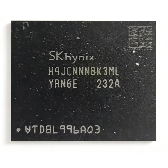
Perbandingan Spesifikasi
| Parameter Umum | H9JCNNNBK3MLYR-N6E-SK | H9JCNNNBK3MLYR-N6E |
|---|---|---|
| Merek | SK hynix | SK hynix |
| Kategori | Memory ICs | Memory ICs |
| Status Lingkungan Hidup | Aktif | Aktif |
| Harga Unit (USD) | — | $24,37 |
| Tipe Memori | Volatile - DRAM (LPDDR5 SDRAM) | LPDDR5 SDRAM |
| Density | 16 Gb (2 GB) | 16 Gb (2 GB) |
| Organisasi | 512M x 32 | 512M x 32 |
| Laju Data | 6400 Mbps (LPDDR5-6400) | 6400 Mbps per pin |
| Bus Width | 16-bit | — |
| Channel Architecture | Dual-channel (per datasheet family) | — |
| VDD (Core Supply) | 1.05 V (range 1.01 V to 1.12 V) | — |
| VDDQ (I/O Supply) | 1.8 V (range 1.7 V to 1.95 V) | — |
| Suhu Kerja | -55C to +125C | [DATA_NEEDED: operating temperature range] |
| Paket | 315-ball TFBGA (12 x 12 mm) | TFBGA-315 |
| Tipe Mounting | Surface Mount | Surface Mount |
| JEDEC Standard | JESD209-5 (LPDDR5) | — |
| On-die ECC | Yes (per LPDDR5 base spec) | — |
| Status RoHS | Compliant | Compliant |
| Level MSL | [DATA_NEEDED: MSL rating] | [DATA_NEEDED: MSL level] |
| Supply Voltage (VDD2) | — | 1.05 V |
| Supply Voltage (VDD1) | — | [DATA_NEEDED: VDD1 rail voltage] |
| Supply Voltage (VDDQ) | — | [DATA_NEEDED: VDDQ rail voltage] |
| Number of Channels | — | Dual channel (x16 + x16) |
| Memory Technology | — | DRAM (volatile) |
| Refresh Mode | — | [DATA_NEEDED: refresh mode support] |
| On-Die Termination | — | [DATA_NEEDED: ODT support] |
| Bank Architecture | — | [DATA_NEEDED: bank group configuration] |