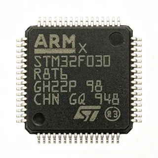
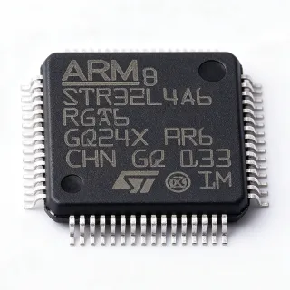
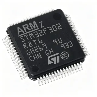
STM32F103RET6TR - 72MHz Cortex-M3, 512KB Flash MCU | STMicroelectronics (Tape & Reel)
MPN: STM32F103RET6TR ✓ AktifSTM32F103RET6TR Ringkasan
What is an ARM Cortex-M3 microcontroller? An MCU (microcontroller unit) integrates a processor core, program memory, data memory, and programmable peripherals on a single die, enabling standalone embedded operation. The Cortex-M3 is a 32-bit RISC core within the ARM Cortex-M family (Cortex-M0, M3, M4, M7), widely adopted for industrial control, medical instruments, and consumer electronics because of its deterministic interrupt latency, nested vectored interrupt controller (NVIC), and rich peripheral ecosystem. Within STMicroelectronics' portfolio, the STM32F1 series sits in the general-purpose performance class between entry-level STM32F0 and mainstream STM32F4 devices.
Key features of the STM32F103RET6TR include 512 KB of Flash organized in 128-bit wide banks for fast code execution, 64 KB of SRAM, two I2C buses, three SPIs, two I2S, one SDIO, five USARTs, a USB 2.0 full-speed device interface, and a CAN 2.0B controller. The high-density Flash architecture supports both in-system programming (ISP) and in-application programming (IAP), and the JTAG/SWD debug interface enables serviceable designs in the field.
Technically, the Cortex-M3 core uses a 3-stage pipeline with single-cycle multiply and hardware divide. The optional memory protection unit (MPU) and 7-channel DMA controller offload data movement from the CPU, while the 16-bit timers can be cascaded into complex PWM and quadrature encoder chains for motor and power conversion.
Typical applications include motor drives and three-phase inverters, PLC I/O modules, medical devices such as blood-glucose meters, industrial communication gateways using CAN or USB, and consumer human-machine interface panels.
When designing with this device, connect VDDA to a clean filtered analog supply and configure BOOT0 correctly at reset, because boot-mode selection directly affects programming and startup behavior. The HSE crystal range (4-16 MHz) and LSE 32.768 kHz crystal must be laid out following ST AN2586 PCB guidelines to avoid radio-frequency interference.
This page synthesizes distributor availability, drop-in second sources such as GD32F103RET6, and practical design notes not found in the manufacturer datasheet, providing engineers a one-stop selection resource.
Alternatif penggantian untuk STM32F103RET6TR — paket yang sama, pin-pada-pin kompatibel. Bagian paket yang berbeda memerlukan kerja ulang PCB diabaikan.
GD32F103RET6
📋 Alternatif referensi (tidak dalam katalog)
APM32F103RET6
📋 Alternatif referensi (tidak dalam katalog)
HK32F103RET6
📋 Alternatif referensi (tidak dalam katalog)
STM32F103RET6TR Rating Maksimal & Karakteristik Listrik
| Core Architecture | ARM Cortex-M3 32-bit RISC |
| Frekuensi Bawah Maximum | 72 MHz |
| Flash Memory | 512 KB |
| SRAM | 64 KB |
| Supply Voltage (VDD) | 2.0 V to 3.6 V |
| Suhu Kerja | -40 C to +85 C (industrial) |
| Paket | LQFP-64 (10x10 mm) |
| GPIO Count | 51 |
| ADC | 3 x 12-bit, up to 21 channels |
| General-Purpose Timers | 4 x 16-bit |
| Advanced PWM Timers | 2 x 16-bit (with complementary outputs) |
| Communication Interfaces | 2 x I2C, 3 x SPI, 2 x I2S, 5 x USART, USB 2.0 FS, CAN 2.0B, SDIO |
| DMA Channels | 7 |
| Debug Interface | JTAG + Serial Wire Debug (SWD) |
| Status RoHS | Compliant |
| Tipe Mounting | Surface Mount |
Konfigurasi Pin STM32F103RET6TR
| Pin produk 1 | VBAT — Backup battery supply for RTC |
| Pin produk 2 | PC13 — GPIO/Tamper-RTC |
| Pin produk 3 | PC14 — GPIO/OSC32_IN |
| Pin produk 4 | PC15 — GPIO/OSC32_OUT |
| Pin produk 5 | OSC_IN — HSE oscillator input |
| Pin produk 6 | OSC_OUT — HSE oscillator output |
| Pin produk 7 | NRST — Reset input, active low |
| Pin produk 8 | VSSA — Analog ground |
| Pin produk 9 | VDDA — Analog supply (2.0-3.6 V) |
| Pin produk 10 | PA0 — GPIO/ADC12_IN0/WKUP |
| Pin produk 11 | PA1 — GPIO/ADC12_IN1 |
| Pin produk 12 | PA2 — GPIO/USART1_TX/ADC12_IN2 |
| Pin produk 13 | PA3 — GPIO/USART1_RX/ADC12_IN3 |
| Pin produk 14 | PA4 — GPIO/SPI1_NSS/ADC12_IN4 |
| Pin produk 15 | PA5 — GPIO/SPI1_SCK/ADC12_IN5 |
| Pin produk 16 | PA6 — GPIO/SPI1_MISO/ADC12_IN6 |
| Pin produk 17 | PA7 — GPIO/SPI1_MOSI/ADC12_IN7 |
| Pin produk 18 | PB0 — GPIO/ADC12_IN8 |
| Pin produk 19 | PB1 — GPIO/ADC12_IN9 |
| Pin produk 20 | PB2 — GPIO/BOOT1 |
| Pin produk 21 | PB10 — GPIO/I2C2_SCL/USART3_TX |
| Pin produk 22 | PB11 — GPIO/I2C2_SDA/USART3_RX |
| Pin produk 23 | VSS_1 — Ground |
| Pin produk 24 | VDD_1 — Digital supply (2.0-3.6 V) |
| Pin produk 25 | PB12 — GPIO/SPI2_NSS |
| Pin produk 26 | PB13 — GPIO/SPI2_SCK |
| Pin produk 27 | PB14 — GPIO/SPI2_MISO |
| Pin produk 28 | PB15 — GPIO/SPI2_MOSI |
| Pin produk 29 | PA8 — GPIO/USART1_CK/TIM1_CH1 |
| Pin produk 30 | PA9 — GPIO/USART1_TX/TIM1_CH2 |
| Pin produk 31 | PA10 — GPIO/USART1_RX/TIM1_CH3 |
| Pin produk 32 | PA11 — GPIO/USBDM/CAN_RX |
| Pin produk 33 | PA12 — GPIO/USBDP/CAN_TX |
| Pin produk 34 | PA13 — GPIO/JTMS-SWDIO |
| Pin produk 35 | VSS_2 — Ground |
| Pin produk 36 | VDD_2 — Digital supply (2.0-3.6 V) |
| Pin produk 37 | PA14 — GPIO/JTCK-SWCLK |
| Pin produk 38 | PA15 — GPIO/JTDI/TIM1_CH3 |
| Pin produk 39 | PB3 — GPIO/JTDO/TRACESWO |
| Pin produk 40 | PB4 — GPIO/JTRST |
| Pin produk 41 | PB5 — GPIO/I2C1_SMBAI |
| Pin produk 42 | PB6 — GPIO/I2C1_SCL/TIM4_CH1 |
| Pin produk 43 | PB7 — GPIO/I2C1_SDA/TIM4_CH2 |
| Pin produk 44 | BOOT0 — Boot mode selection at reset |
| Pin produk 45 | PB8 — GPIO/TIM4_CH3 |
| Pin produk 46 | PB9 — GPIO/TIM4_CH4 |
| Pin produk 47 | VSS_3 — Ground |
| Pin produk 48 | VDD_3 — Digital supply (2.0-3.6 V) |
| Pin produk 49 | PE0 — GPIO/TIM4_ETR |
| Pin produk 50 | PE1 — GPIO |
| Pin produk 51 | PE2 — GPIO/TRACECK |
| Pin produk 52 | PE3 — GPIO/TRACED0 |
| Pin produk 53 | PE4 — GPIO/TRACED1 |
| Pin produk 54 | PE5 — GPIO/TRACED2 |
| Pin produk 55 | PE6 — GPIO/TRACED3 |
| Pin produk 56 | PE7 — GPIO |
| Pin produk 57 | PE8 — GPIO/TIM1_CH1N |
| Pin produk 58 | PE9 — GPIO/TIM1_CH1 |
| Pin produk 59 | PE10 — GPIO/TIM1_CH2N |
| Pin produk 60 | PE11 — GPIO/TIM1_CH2 |
| Pin produk 61 | PE12 — GPIO/TIM1_CH3N |
| Pin produk 62 | PE13 — GPIO/TIM1_CH3 |
| Pin produk 63 | PE14 — GPIO/TIM1_CH4 |
| Pin produk 64 | PE15 — GPIO/TIM1_BKIN |
Aplikasi Umum
STM32F103RET6TR cocok untuk 6 aplikasis: Brushless DC Motor Drive, Industrial CAN Gateway, Medical Blood-Glucose Meter, PLC Digital I/O Module, USB Human Interface Device, Consumer HMI Touch Panel.
Brushless DC Motor Drive
The STM32F103RET6TR fits three-phase BLDC and PMSM motor drives because its two advanced 16-bit timers provide complementary PWM outputs with programmable dead-time insertion, while the 72 MHz Cortex-M3 executes field-oriented control loops in well under 10 us. The three 12-bit ADCs sample phase currents simultaneously at 1 us conversion rates, and the CAN 2.0B interface streams telemetry to a vehicle or industrial controller. A typical 1 kW inverter running FOC at 20 kHz PWM leaves ample CPU margin to host a small RTOS for fault handling and encoder feedback.
Direkomendasikan
Industrial CAN Gateway
The STM32F103RET6TR serves CAN-to-USB and CAN-to-Ethernet gateway applications because it integrates a bxCAN 2.0B interface, a USB 2.0 full-speed device, and five USARTs without external bridge chips. The 512 KB Flash holds a CANopen or J1939 stack alongside the gateway logic, while the 64 KB SRAM buffers CAN frames at 1 Mbit/s bus loads. The Cortex-M3 NVIC handles time-critical CAN RX interrupts deterministically within 12 cycles, which is essential for industrial protocols that drop frames on jitter.
Direkomendasikan
Medical Blood-Glucose Meter
The STM32F103RET6TR is widely used in handheld medical meters because the 72 MHz core runs electrochemical sensor algorithms in real time while the 12-bit ADC reads picoampere-scale currents through on-chip amplifiers. The low-power Run, Sleep, and Stop modes (down to ~10 uA in Standby) extend battery life across multi-month shelf-life targets, and the USB 2.0 FS device interface charges the battery and uploads logs to a PC. The 512 KB Flash stores reference tables, calibration curves, and a small UI library for the LCD interface.
Direkomendasikan
PLC Digital I/O Module
The STM32F103RET6TR fits 32-channel PLC digital I/O modules because its 51 GPIO drive opto-isolated inputs and relay coils directly, while its 7 DMA channels offload filter debouncing and pulse counting without CPU intervention. The five USARTs and one CAN bus link to the fieldbus master, and the Cortex-M3 executes ladder-logic interpretation or IEC 61131-3 soft-PLC runtimes in 512 KB Flash with comfortable margin. Industrial -40 C to +85 C operation matches IEC 60068 cabinet specifications.
Direkomendasikan
USB Human Interface Device
The STM32F103RET6TR is ideal for USB HID peripherals such as custom keyboards, foot controllers, and industrial pendants because the on-chip USB 2.0 full-speed device controller, 72 MHz CPU, and 512 KB Flash hold the USB stack plus HID report logic with no external PHY. The five USARTs and timers can drive LED indicators and rotary encoders concurrently, and the 12-bit ADC reads potentiometer position at 1 MSps. ST's USB Device Library provides ready HID, CDC, and DFU class examples for quick bring-up.
Direkomendasikan
Consumer HMI Touch Panel
The STM32F103RET6TR drives small TFT touch panels because the three SPIs drive LCD controllers at 36 MHz, and the 12-bit ADC reads a resistive touch overlay with on-chip timers handling periodic sampling via DMA. The 512 KB Flash stores LVGL graphics plus fonts, while the 64 KB SRAM holds double-buffered 320x240 RGB framebuffers. The SDIO interface streams images from a microSD card, and the CAN or USART connects to the host appliance.
Direkomendasikan
Ringkasan Produk Direkomendasikan
Data referensi engineering untuk STM32F103RET6TR — pembandingan, panduan desain, dan informasi konformitas.
Panduan Pemilihan
Pembandingan dengan Alternatif
| Parameter Umum | Produk Ini | STM32F103RBT6 | STM32F103RCT6 | STM32F103RGT6 | GD32F103RET6 | APM32F103RET6 |
|---|---|---|---|---|---|---|
| Package | LQFP-64 | LQFP-64 - same | LQFP-64 - same | LQFP-64 - same | LQFP-64 - same | LQFP-64 - same |
| Brand | STMicroelectronics | STMicroelectronics | STMicroelectronics | STMicroelectronics | GigaDevice | Geehy |
| Core / Max Clock | Cortex-M3 / 72 MHz | Cortex-M3 / 72 MHz | Cortex-M3 / 72 MHz | Cortex-M3 / 72 MHz | Cortex-M3 / 108 MHz | Cortex-M3 / 72 MHz |
| Flash | 512 KB | 128 KB | 256 KB | 1 MB | 512 KB | 512 KB |
| SRAM | 64 KB | 20 KB | 48 KB | 96 KB | 64 KB | 64 KB |
| GPIO | 51 | 51 | 51 | 51 | 51 | 51 |
| USB / CAN | USB FS device + CAN 2.0B | USB FS + CAN | USB FS + CAN | USB FS + CAN | USB FS + CAN | USB FS + CAN |
| Operating Temperature | -40 C to +85 C | -40 C to +85 C | -40 C to +85 C | -40 C to +85 C | -40 C to +85 C | -40 C to +85 C |
| Approx. Unit Price (qty-1, USD) | 8.20 | ~5.40 | ~6.50 | ~9.80 | ~3.10 (LCSC) | ~3.40 (LCSC) |
Diferensiator Kunci
- Largest Flash density in 64-pin LQFP STM32F1 line (vsSTM32F103RBT6)
- Proven ecosystem with mature firmware libraries (vsGD32F103RET6)
- Stable industrial-grade supply vs volatile gray-market (vsGD32F103RET6)
Catatan Desain
Place 100 nF X7R ceramic bypass capacitors on every VDD pin (pins 24, 36, 48) within 2 mm of the package pad. Add a single 4.7 uF bulk capacitor on the VDD rail. The VDDA analog supply must be filtered through a ferrite bead and decoupled with 100 nF plus 1 uF to keep ADC noise below 1 LSB at 12-bit resolution, per ST application note AN2586 reference layouts.
Route the HSE 8 MHz crystal traces (OSC_IN at pin 5, OSC_OUT at pin 6) symmetrically and shield them with a ground guard ring; keep the crystal within 5 mm of the MCU and the load capacitors (typically 20 pF) returned to a quiet analog ground. Place the 32.768 kHz LSE crystal (PC14/PC15) similarly on the opposite PCB edge to avoid coupling with HSE through the substrate.
Do not leave BOOT0 (pin 44) floating - tie it through a 10 kOhm resistor to VSS for normal Flash boot, or to VDD for system memory bootloader (USART1 DFU) mode. A floating BOOT0 is the single most common reason new boards fail to program. Also ensure NRST (pin 7) has a 100 nF capacitor to VSS and a 10 kOhm pull-up to VDD for clean reset behavior under 1.8 V brown-out.
The STM32F103RET6TR in LQFP-64 has a theta_JA of approximately 65 C/W on a 4-layer JEDEC PCB. At 72 MHz with all peripherals active, core current is ~50 mA (3.3 V x 0.050 A = 165 mW), so junction temperature rise is ~7 C above ambient - well within the 85 C industrial ceiling. No thermal copper pour is required for normal operation, though a 1 cm2 ground pour improves long-term reliability.
The USB DP/DM traces (PA11/PA12) must be 90 ohm differential, length-matched within 2 mm, and routed over a continuous ground plane. Place the 22 ohm series termination resistors close to the MCU pins. For EMI, add a common-mode choke on the USB cable side if the design will pass CE/FCC. CAN bus traces (PA11/PA12 alternate function) require 120 ohm termination at each bus end.
Informasi Konformitas
RoHS compliant per ST product page. Industrial -40 C to +85 C grade; not AEC-Q100 qualified - migrate to STM32G0/G4 for automotive. Halogen-free per ST materials declaration.