ディスクリート半導体
サブカテゴリ
製品 (1814)

CDBQR0230L-HF - 30V 200mA Schottky Diode | Comchip | 0402
The Comchip Technology CDBQR0230L-HF is a 30V, 200mA surface-mount Schottky barrier diode housed in a compact 0402/SOD-923F package. It features a low forward voltage drop and fast switching characteristics typical of Schottky technology, with a VR (reverse voltage) rating of 30V and an Io (average rectified output current) rating of 200mA. A Schottky barrier diode is a semiconductor device formed by a metal-semiconductor junction rather than a PN junction, which produces a lower forward voltage drop (typically 0.3V to 0.5V vs 0.7V for a silicon diode) and faster switching speed at the expense of higher reverse leakage current. In the power management hierarchy, Schottky diodes sit under discrete semiconductors -> diodes -> rectifier diodes -> Schottky diodes -> power management components, and are widely used for low-voltage rectification, reverse polarity protection, and signal clamping. Key features of the CDBQR0230L-HF include its ultra-small 0402 footprint (SOD-923F), which is among the smallest standard diode packages, RoHS compliance for environmental compatibility, and a low forward voltage drop that minimizes conduction losses in low-voltage circuits. The device is suitable for high-density PCB designs where board space is at a premium. The CDBQR0230L-HF uses Schottky barrier technology with a low barrier height, enabling fast switching and low forward voltage. Its compact form factor makes it ideal for portable and wearable electronics where every square millimeter of PCB counts. The 30V reverse voltage rating provides adequate headroom for 5V and 12V rails, while the 200mA current rating suits signal-level and low-power applications. Typical applications include reverse polarity protection in portable devices, low-voltage rectification in DC-DC converters, freewheeling diode in small switching circuits, signal clamping and OR-ing, and ESD protection augmentation in USB and battery interfaces. The 0402 footprint is well-suited for hand-held, IoT, and wearable product designs. When designing with the CDBQR0230L-HF, ensure the thermal path is adequate. Although the 200mA current is modest, the small 0402 package has limited thermal dissipation; sustained current near the maximum rating will require attention to copper pad sizing on the PCB. The HF suffix denotes Halogen-Free, which is important for environmental compliance. This page synthesizes distributor pricing, drop-in alternatives, and practical design notes not found in the manufacturer datasheet alone, helping engineers select the right Schottky diode for compact, low-power designs.

CDDFN2-T3V3SC - 3.3V Bidirectional TVS Diode, DFN-2 | Bourns
The Bourns CDDFN2-T3V3SC is a 3.3 V bidirectional surface-mount Transient Voltage Suppressor (TVS) housed in a sub-miniature DFN-2 (0402-size, 1.0 mm x 0.6 mm x 0.5 mm) package. It delivers ESD, EFT and surge protection for external ports of portable electronic devices and provides a typical clamping voltage of 9 V at 42 A peak pulse current (8/20 us waveform). The device is designed for direct PCB mounting on high-density I/O lines where a board area is impossible. A TVS diode is a semiconductor clamp that diverts over-voltage energy away from sensitive downstream circuitry. When the line voltage exceeds the device's breakdown threshold, the TVS enters avalanche breakdown within nanoseconds and shunts the transient current to ground, limiting the peak voltage seen by the protected IC. TVS diodes sit at the first tier of a protection scheme (next to gas-discharge tubes and PTC fuses) and are the fastest-responding element, making them ideal for suppressing ESD (electrostatic discharge) and EFT (electrical fast transient) events at connector pins. As a discrete protection component, the TVS diode belongs to the broader family of surge protection devices used in transient voltage suppression. Key specifications include a 3.3 V working voltage (VRWM), 9 V typical clamping voltage (VC) at 42 A Ipp (8/20 us), bidirectional polarity, and a sub-nanosecond response time. The DFN-2 (0402-style) package occupies 0.6 mm footprint area per side and operates across -55 C to +150 C. It is qualified to IEC 61000-4-2 (ESD) air-discharge ratings typical of the family, and the device is RoHS compliant and lead-free. The CDDFN2-T3V3SC uses a silicon avalanche junction in a bidirectional configuration, meaning a single device protects both polarities of an AC or differential data line. The 8/20 us surge waveform rating indicates the device can survive indirect lightning-induced surges and inductive load switching transients without degradation. Typical applications include USB 2.0/3.0 data line protection, HDMI/MIPI/MDDI interfaces, SIM card protection, headset/microphone audio jacks, portable set buttons, and any 3.3 V logic rail exposed to user contact. The DFN-2 footprint makes it especially suitable for compact handheld and wearable designs where every millimeter of PCB space counts. When designing with the CDDFN2-T3V3SC, ensure the protected signal line does not exceed the 3.3 V working voltage in normal operation, place the device as close as physically possible to the connector pin, and provide a low-impedance ground return directly beneath the package thermal pad. The device's low capacitance makes it compatible with high-speed data lines, but always verify the total channel capacitance against the interface specification.
CDDFN2-T5V0SC - 5V Bidirectional TVS Diode, 9.5V Clamp | Bourns
The Bourns CDDFN2-T5V0SC is a bidirectional surface-mount Transient Voltage Suppressor (TVS) diode rated at 5 V working voltage with a 9.5 V clamping voltage at 18 A peak pulse current (8/20 µs waveform), housed in a miniature 2-pin DFN (1.0 × 0.6 mm) package. It is engineered to absorb ESD, EFT, and surge transients on external I/O ports of portable and handheld electronics, and integrates a steering diode network for clean bidirectional clamping from either polarity. A Transient Voltage Suppressor (TVS) diode is a clamping semiconductor device designed to limit transient overvoltages by avalanching into a low-impedance state when its breakdown voltage is exceeded. Within the power management hierarchy, TVS diodes sit alongside ESD protection arrays and varistors as the first line of defense for sensitive downstream ICs, providing sub-nanosecond response and a defined non-linear V-I curve. Bidirectional TVS parts such as the CDDFN2-T5V0SC are particularly suited to AC-coupled signal lines and differential data buses where polarity can reverse. The CDDFN2-T5V0SC delivers 18 A peak pulse handling on the 8/20 µs surge waveform and is rated to absorb ESD strikes per IEC 61000-4-2 at both contact and air discharge levels. Its ultra-small 1.0 × 0.6 mm DFN footprint allows placement immediately at the connector, minimizing parasitic loop area and improving coupling efficiency into the suppressor. Low clamping factor and low dynamic resistance keep the residual voltage seen by downstream ICs well below their absolute-maximum ratings. Internally the device uses a Zener-based avalanche junction combined with a steering-diode bridge, giving symmetric positive and negative clamping. The low leakage at 5 V bias preserves battery life in always-connected portable designs, while the wide operating temperature range supports industrial and outdoor deployments. The leadless DFN-2 package offers a low-inductance current path that outperforms leaded alternatives such as SOD-123 at multi-kilovolt ESD. Typical applications include USB Type-C data line protection on smartphones, tablets, and laptops, HDMI/MIPI/LVDS interface protection on display panels, antenna port ESD protection on cellular and Wi-Fi modules, headset audio jack protection, and portable medical handheld devices. The wide surge rating also covers industrial sensor interfaces and IoT edge nodes that may be exposed to EFT or lightning-induced surges on long cable harnesses. Place the CDDFN2-T5V0SC as close as physically possible to the external connector pin, with a short, direct ground return to the chassis or board ground pour. Keep the trace between the protected line and the device under 2 mm to maximize ESD suppression, and avoid routing any sensitive analog signal traces underneath the pad to prevent coupling of residual transients. This page synthesizes distributor pricing tiers, verified drop-in alternatives, and PCB-layout guidance that go beyond what is shown on the Bourns datasheet, giving engineers a single source for selection, sourcing, and design-in.
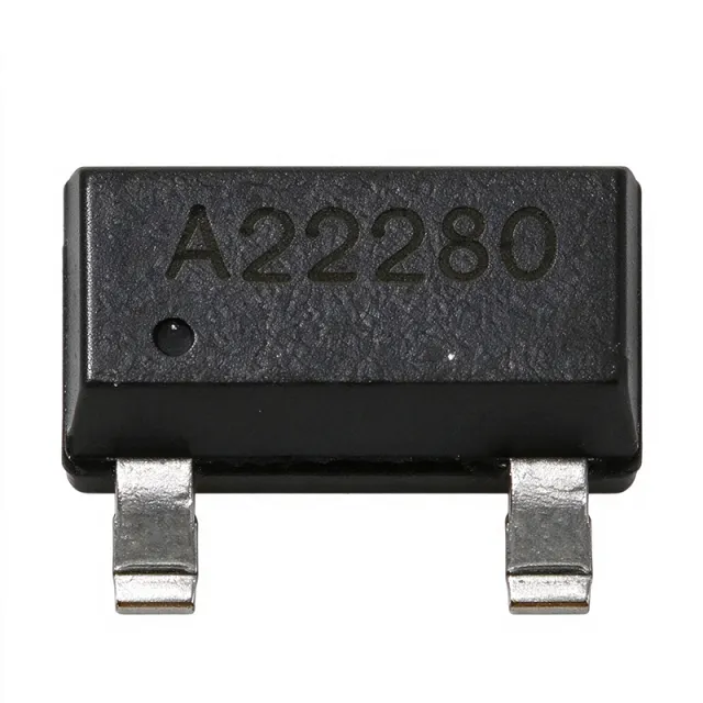
CDSOT23-SM712 - 7V/12V Asym RS-485 TVS Array 400W | Bourns
The Bourns CDSOT23-SM712 is a surface-mount transient voltage suppressor (TVS) diode array housed in a SOT-23-3 package, providing 400 W peak pulse power per line for asymmetrical protection of RS-485/RS-422 data lines. The device integrates two TVS diodes with a Working Peak Reverse Voltage of 7 V (positive side) and 12 V (negative side), Minimum Breakdown Voltage of 7.5 V and 13.3 V respectively, and maximum clamping voltages of 14 V and 26 V at 17 A (8/20 us waveform). The asymmetry is intentional - it tracks the wider negative common-mode range of RS-485 transceivers that must tolerate -7 V to +12 V. A TVS diode array is a specialized class of transient voltage suppressor that integrates multiple steering/clamps in one package to protect differential data ports. The CDSOT23-SM712 belongs to the diode array > TVS array > ESD protection IC > circuit protection hierarchy. These arrays are essential companions to bus transceivers (RS-485, CAN, Profibus), where the transceiver's own absolute-maximum ratings are routinely violated by ESD, EFT, or surge events on the bus cable. Key features include IEC 61000-4-2 (ESD) protection to +/-30 kV air and +/-30 kV contact, IEC 61000-4-4 (EFT) to 40 A (5/50 ns), and IEC 61000-4-5 (surge) to 17 A (8/20 us). The device provides low capacitance (per datasheet typical application) to preserve signal integrity at high data rates, and the SOT-23-3 footprint is the industry-standard pinout for SM712-style arrays. A low leakage current at 5 V maximises battery life in quiescent-mode industrial nodes. The CDSOT23-SM712 uses an asymmetric avalanche-breakdown architecture: the 7 V TVS clamps positive transients on each data line relative to ground, while the 12 V TVS clamps the larger negative excursions permitted by RS-485. This dual-window topology is more efficient than two identical TVS diodes, because a single 12 V symmetric array would clip legitimate -7 V bus signalling, while a 7 V symmetric array would not survive the -25 V cable discharge that the RS-485 standard tolerates. The Bourns design matches the SM712 reference footprint exactly, so engineers can swap between vendors (Bourns, ST, NXP, MSKSEMI, YINT) without PCB rework. Typical applications include RS-485/RS-422 fieldbus nodes in industrial automation, Profibus and Modbus links, CAN bus nodes in heavy machinery and EV charging, HVAC controllers, building automation, smart-meter communication ports, and any line-driver exposed to ESD during cable mating or lightning-induced surge on long outdoor runs. The asymmetrical window is also useful for CAN-H and CAN-L protection where one rail must withstand -12 V cross-wiring faults. When designing with this device, place the CDSOT23-SM712 within 10 mm of the bus connector and keep the ground return path short and wide. Do not rely on the TVS alone for surge survival above 17 A - upstream PTCs or PTC+fuse combinations may be required to meet IEC 61000-4-5 level 4. The SOT-23-3 pad pattern is identical to industry-standard SOT-23, allowing use of standard land pattern footprints. This page synthesizes distributor pricing, drop-in alternatives, and practical PCB layout notes not found in the manufacturer datasheet alone - including a same-package alternative table engineers can use when second-sourcing for supply-chain resilience.

CDSOT23-T24CAN-Q - 24V CAN Bus TVS, 40V Clamp, AEC-Q101 | Bourns
The Bourns CDSOT23-T24CAN-Q is a dual bidirectional TVS diode array for CAN bus protection, offering a 40 V clamping voltage, 8 A (8/20 us) peak pulse current, and a minimum breakdown voltage of 26.2 V, housed in a 3-pin SOT-23 (SOT-23-3) surface-mount package. It is AEC-Q101 qualified for automotive applications. A TVS (Transient Voltage Suppressor) diode is a circuit-protection semiconductor that clamps transient overvoltage events, such as electrostatic discharge (ESD) and surge transients, by avalanche breakdown before they can damage sensitive transceiver circuitry. Within the protection hierarchy, TVS diode arrays sit at the board level of a layered protection strategy, complementing chip-level protection integrated inside the CAN transceiver itself. Arrays like this one integrate two TVS elements in a single package so that both lines of a differential bus are protected by one component. Key features include the dual bidirectional topology purpose-built for CANH and CANL differential lines, a minimum breakdown voltage of 26.2 V that guarantees the device will not conduct during a 24 VDC power-cross miswiring event, and a 40 V clamping voltage at the 8 A (8/20 us) surge level. The AEC-Q101 qualification ensures reliability under automotive stress conditions. The device uses avalanche breakdown diode technology with a low-clamping, fast-response characteristic. Because the protection elements are bidirectional, they clamp negative transients symmetrically on both CAN lines, protecting the transceiver differential I/O against ISO 7637-style and IEC 61000-4-5 style surge events referenced in Bourns CANbus application notes. Typical applications include automotive CAN bus nodes, body control modules, industrial CANopen and DeviceNet networks, and 24V truck and off-highway vehicle bus systems where 24 V power miswiring tolerance is mandatory. Design consideration: place the TVS array as close as possible to the connector with short, wide low-inductance traces to ground so the clamping path stays effective at fast transient edge rates. This page synthesizes distributor availability, verified drop-in alternatives, and practical CAN protection design guidance not found in the manufacturer datasheet.
CDSOT23-T24CAN-Q-X - 24V CANbus TVS Protector | Bourns
The Bourns CDSOT23-T24CAN-Q-X is an AEC-Q101-qualified dual bidirectional TVS diode array CANbus protector in a 3-pin SOT-23 package, rated for 8 A (8/20 us) Ipp surge current, 40 V clamp voltage, and a minimum breakdown voltage of 26.2 V so it does not conduct during a 24 VDC power cross event. A CANbus protector is a specialized transient voltage suppression (TVS) diode array that clamps electrostatic discharge (ESD) and surge transients on the two differential data lines of a Controller Area Network (CAN) interface. TVS arrays belong to the broader circuit protection family of semiconductors, which also includes varistors, gas discharge tubes, and surge protectors. On the signal-chain hierarchy, the protector sits between the CAN transceiver pins and the physical bus wiring, diverting fault energy to ground before it can damage sensitive silicon. Key features of the CDSOT23-T24CAN-Q series include AEC-Q101 automotive-grade qualification, surge immunity per IEC 61000-4-5 (Level 1), and ESD robustness beyond IEC 61000-4-2 up to 30 kV. The dual bidirectional topology protects both CANH and CANL lines with a single SOT-23 component, minimizing board area and stray inductance. The 26.2 V minimum breakdown voltage is deliberately chosen so the device remains idle during 24 VDC power cross faults common in industrial and truck installations. Technically, the device uses two bidirectional avalanche diodes sharing a common ground pin. Under a +500 V surge event, Bourns clamp voltage measurements in the datasheet show conduction at approximately 40 V clamp rating at the specified Ipp, keeping the voltage at the transceiver pins well below typical absolute maximum ratings. Bidirectional clamping handles both positive and negative surge polarities without polarity-sensitive installation. Typical applications include CANbus transceiver protection in automotive body and powertrain ECUs, 24V industrial CAN networks in factory automation, and CAN interfaces on trucks, agricultural machinery, and battery management systems where 24 V power cross events must be tolerated. When designing with this device, place it as close as possible to the CAN connector, with a short, wide ground return path; the series termination resistors should sit between the protector and the transceiver to limit peak diode current. This page adds information gain beyond the manufacturer datasheet by synthesizing distributor availability, verified drop-in alternatives including the NXP PESD2CAN cross reference, and practical CANbus layout guidance in one place.

CGD65A055S2 - 650V 55mΩ GaN HEMT with ICeGaN Gate | Cambridge GaN Devices
The Cambridge GaN Devices CGD65A055S2 is an enhancement-mode GaN-on-silicon power transistor rated at 650 V drain-to-source voltage and 55 mΩ on-resistance, delivered in a 16-pin DFN 8x8 surface-mount package. The part exploits the unique wide-bandgap properties of gallium nitride to achieve high current capability (27 A pulsed), high breakdown voltage, and high switching frequency operation in a single chip-scale footprint. What is a GaN HEMT? A GaN HEMT (Gallium Nitride High Electron Mobility Transistor) is a wide-bandgap field-effect transistor built on an AlGaN/GaN heterojunction. Compared with traditional silicon MOSFETs, GaN HEMTs offer lower on-resistance per unit area, zero reverse-recovery charge (Qrr), and much faster switching edges. They belong to the broader hierarchy of power semiconductors (power transistor → FET → HEMT → GaN HEMT → wide-bandgap device) and are typically deployed in switched-mode power supplies (SMPS), where they enable higher power density and efficiency than silicon super-junction MOSFETs. Key features of the CGD65A055S2 include CGD's proprietary ICeGaN™ gate technology, which makes the device directly compatible with virtually all standard gate drivers and controller ICs without requiring a negative-rail bias supply. The device integrates a current-sense (CS) pin that outputs a proportional signal of the drain current, eliminating the need for an external shunt resistor in many topologies. An integrated NL³ (non-linear, low-loss, low-R) circuit reduces dead-time losses in half-bridge configurations, improving overall converter efficiency. Typical applications include totem-pole bridgeless PFC, LLC and QR flyback converters, half-bridge and full-bridge motor drivers, on-board chargers (OBC), telecom rectifier modules, and Class-D audio amplifiers where audio-grade linearity and high dV/dt immunity are required. The 650 V rating provides generous derating margin for universal-input AC/DC converters operating from rectified 230 VAC mains. When designing with this device, ensure the gate-drive loop inductance is minimized to keep switching edges clean. Use a 4.7-10 Ω external gate resistor and Kelvin-source connection where available. Place a small ferrite bead or RC snubber on the switching node to damp high-frequency ringing caused by the very fast dV/dt capability of the GaN die.
CGD65A055SH2 - 650V 55mΩ GaN HEMT ICeGaN® H2 | CGD
The Cambridge GaN Devices CGD65A055SH2 is a 650 V, 55 mΩ enhancement-mode GaN-on-silicon power transistor from the ICeGaN® H2 family, integrating ICeGaN® gate technology, integrated current-sense, and NL³ (no-leakage, low-loss) circuitry in a 16-DFN (8x8) surface-mount package. It delivers a continuous drain current of 27 A at 25 °C, gate charge of 4 nC at VGS = 12 V, and switching speeds an order of magnitude faster than silicon MOSFETs at the same R_DS(on). A GaN HEMT (Gallium Nitride High Electron Mobility Transistor) is a wide-bandgap power semiconductor that exploits the high electron mobility and high critical electric field of GaN to deliver lower on-resistance per unit area, lower switching losses, and higher switching frequencies than equivalent silicon MOSFETs. The CGD65A055SH2 belongs to the discrete semiconductors > MOSFETs category and is increasingly used as a silicon-MOSFET replacement in switched-mode power conversion. Key features include a 650 V drain-source breakdown rating, integrated current sensing that eliminates external sense resistors, an embedded NL³ circuit that suppresses unwanted turn-on and reduces parasitic-induced losses, and an ICeGaN® interface that provides a clean, well-defined gate drive behavior despite GaN's normally-on heritage. The 16-DFN (8x8) package offers an exposed thermal pad for low junction-to-PCB thermal resistance and is fully compatible with surface-mount reflow assembly. Technically, the device uses a GaN-on-silicon epi structure with a normally-off cascode-style gate arrangement, achieving clean threshold behavior near 1-2 V typical with a recommended drive level of VGS = 12 V. The integrated current-sense pin mirrors a portion of drain current to an external resistor for cycle-by-cycle or average-current control, simplifying implementation of OCP/OCM without the cost, footprint, or noise penalty of a discrete shunt. Typical applications include AC-DC totem-pole PFC stages in EV chargers, server SMPS primary-side switches, industrial motor drives, Class-D audio amplifiers, photovoltaic micro-inverters, and USB-PD adapters above 100 W. Where efficiency and power density are paramount, the CGD65A055SH2's combination of low R_DS(on), low Qg, and integrated features removes several passive components from the BOM. When designing with this part, gate-drive discipline is critical: use a clean 12 V supply with low impedance and tight dv/dt control to avoid unwanted Miller-induced turn-on. Pair the CGD65A055SH2 with a properly sized thermal copper pour to take advantage of the low RDS(on) at high currents, and always reference the manufacturer layout guidelines for source-inductance minimization. This page synthesizes distributor pricing, drop-in alternatives, and practical GaN-specific design notes not found in the manufacturer datasheet, giving power engineers a single source for selection, sourcing, and application guidance.
CGD65A130S2 - 650V 130mΩ GaN HEMT | Cambridge GaN Devices
The Cambridge GaN Devices CGD65A130S2 is a 650V, 130 mΩ enhancement-mode GaN-on-silicon power transistor housed in a DFN-16 (8×8 mm) surface-mount package. It is engineered to deliver high current capability, high breakdown voltage, and high switching frequency for demanding power-conversion applications where silicon MOSFETs are increasingly limited by their switching-loss floor. What is a GaN HEMT? A Gallium Nitride High-Electron-Mobility Transistor (GaN HEMT) is a wide-bandgap power device in which a two-dimensional electron gas (2DEG) is formed at the AlGaN/GaN heterojunction. Compared to silicon MOSFETs, GaN HEMTs offer higher electron mobility, lower output capacitance, zero reverse-recovery charge, and roughly an order-of-magnitude lower gate charge, enabling much smaller and more efficient switched-mode power supplies. Within the power-semiconductor hierarchy, GaN HEMTs sit between traditional silicon MOSFETs and emerging SiC MOSFETs, and they belong to the wider class of wide-bandgap (WBG) semiconductors. The CGD65A130S2 features CGD's proprietary ICeGaN™ gate technology, which delivers a robust gate structure tolerant to wide gate-drive swings (typically up to ±20 V on the gate) and is compatible with virtually all standard gate drivers and controller ICs. Designers can therefore drop this part into existing silicon-MOSFET footprints without redesigning the gate-drive circuitry. The device integrates current-sense and Miller-clamp (NL³) functionality that simplifies protection design in half-bridge and full-bridge topologies. Designed for high-frequency operation up to several hundred kHz with minimal switching loss, the CGD65A130S2 enables substantial reductions in magnetics size, output-capacitor count, and heatsink mass in AC-DC, DC-DC, and PFC converters. The 650V rating provides generous derating margin when fed from 400V PFC rails typical of universal-input offline converters, and the low gate charge and zero Qrr translate directly into higher efficiency at elevated switching frequencies. Typical applications include totem-pole bridgeless PFC front ends for server and telecom SMPS, high-frequency LLC and hard-switched half-bridge converters in industrial PSUs, EV on-board chargers (OBCs) and DC-DC stages, Class-D audio amplifiers, and compact USB-PD chargers and adapters. Designers targeting >200 kHz operation benefit most from the CGD65A130S2's low charge figures. When designing with this part, ensure the gate-drive negative rail stays within the ICeGaN datasheet absolute maximums and respect the exposed-pad PCB-layout recommendations to keep the channel-to-ambient thermal resistance (RθJA) low enough for continuous high-current operation. This page synthesizes distributor pricing, drop-in alternative recommendations, and practical design notes not found in the Cambridge GaN Devices datasheet alone — combining first-party manufacturer specifications with curated engineering guidance for accelerated design-in.
CGD65A130SH2 - 650V GaN HEMT 12A 55mΩ ICeGaN | Cambridge GaN Devices
The Cambridge GaN Devices CGD65A130SH2 is an enhancement-mode GaN-on-silicon power transistor rated at 650 V drain-to-source voltage and 12 A continuous drain current, with a typical on-resistance of 55 mΩ, housed in a 16-pin DFN (8x8 mm) surface-mount package with exposed thermal pad. The device uses CGD's proprietary ICeGaN® gate technology, which provides a 5 V gate-threshold compatibility window so that the part can be driven directly by virtually any standard Si MOSFET gate driver or controller without negative bias or special gate-driver circuitry. A GaN HEMT (Gallium Nitride High Electron Mobility Transistor) is a wide-bandgap power transistor that uses an AlGaN/GaN heterostructure to form a two-dimensional electron gas (2DEG) channel. Compared with silicon MOSFETs, GaN HEMTs offer dramatically lower output capacitance, near-zero reverse-recovery charge, and switching speeds in the MHz range, making them suited for high-frequency, high-density power conversion. The CGD65A130SH2 sits in the power-management hierarchy as a discrete GaN switch used as the main power element in high-frequency switched-mode power supplies (SMPS), motor drives, and photovoltaic inverters. Key features of the CGD65A130SH2 include 650 V drain-source breakdown, 55 mΩ typical R_DS(on), ICeGaN® compatibility with standard 5 V gate drivers, integrated current-sense (CS) pin, and the NL³ (Non-Linear Loss Limiting) circuit that maintains low drive losses even at very high switching frequencies. The wide gate-threshold window and built-in current sensing simplify layout by reducing the need for external shunt resistors and isolated gate-drive bias supplies. Typical application circuits include 65 W to 500 W USB-PD chargers, totem-pole PFC (power factor correction) front ends for server and telecom rectifiers, half-bridge LLC and quasi-resonant converters for high-density AC/DC adapters, photovoltaic micro-inverters, and motor-drive half-bridges. The integrated current-sense output also enables cycle-by-cycle current limiting and over-current protection without an external shunt. This page synthesises distributor pricing, distributor stock, drop-in alternatives analysis, and CGD reference-design guidance that complement the manufacturer datasheet. When designing with CGD65A130SH2, ensure the gate-driver pull-up meets the ICeGaN® gate-charging requirements and that the PCB returns have low inductance to control ringing in the MHz switching range. The 16-DFN exposed pad must be soldered to a sufficient copper pour to keep R_DS(on) stable and junction temperature within rated limits.

CGD65B130S2 - 650V 130mΩ GaN HEMT | Cambridge GaN Devices
The Cambridge GaN Devices CGD65B130S2 is an enhancement-mode GaN-on-silicon power transistor that exploits the unique material properties of gallium nitride to deliver high current, high breakdown voltage, and high switching frequency for a wide range of electronics applications. The part is rated at 650 V drain-source voltage, 130 mΩ on-resistance (typical), with 12 A continuous drain current capability, housed in an 8-pin DFN 5x6 mm surface-mount package with an exposed thermal pad. A GaN HEMT (Gallium Nitride High Electron Mobility Transistor) is a wide-bandgap power transistor that uses an AlGaN/GaN heterostructure to form a high-mobility two-dimensional electron gas (2DEG) channel. Compared to silicon MOSFETs, GaN HEMTs offer 10x higher breakdown field strength, lower on-resistance per unit area, zero reverse-recovery charge (Qrr), and sub-nanosecond switching capability. The CGD65B130S2 belongs to the discrete GaN FET category within the broader power semiconductor hierarchy: GaN HEMT → wide-bandgap transistor → power transistor → discrete semiconductor. Key features include CGD's proprietary ICeGaN™ gate technology that allows the device to be driven directly by virtually any standard gate driver or controller IC without negative bias or external protection circuits. The transistor delivers sub-nanosecond rise/fall times, eliminating the need for gate-drive transformers in many designs. The DFN 5x6 package provides an ultra-low thermal resistance path via the exposed pad, supporting sustained high-current operation. Zero Qrr enables hard-switched half-bridge topologies without the reverse-recovery losses that plague silicon MOSFETs. The architecture combines a normally-off enhancement-mode GaN-on-Si stack with integrated ESD protection and a robust gate clamp, simplifying inverter and PFC design. Compared to equivalent 650V silicon MOSFETs, the CGD65B130S2 reduces switching losses by approximately 50-70 percent, enabling higher switching frequencies (500 kHz to 1 MHz) and smaller magnetics. The device is suitable as a drop-in upgrade path for designers seeking efficiency gains over legacy superjunction MOSFETs. Typical applications include 65W to 500W AC-DC power supplies, totem-pole PFC circuits, LLC and QR flyback converters for USB-PD adapters, photovoltaic microinverters, audio amplifiers, and synchronous rectification in telecom / server PSUs. The high frequency capability is especially valuable in compact USB-PD 3.1 chargers where power density is paramount. When designing with this device, ensure the gate drive swings between 0 V and 10-12 V with minimal overshoot, and keep the high-current power loop (DC+ → high-side FET → low-side FET → DC-) as tight as physically possible to minimize parasitic inductance. Use a Kelvin source connection when available to keep the gate-drive loop separate from the high-current path. This page synthesizes distributor pricing, drop-in alternatives, and practical design notes not typically found in the manufacturer datasheet alone.
CGD65B130SH2 - 650V, 12A GaN HEMT, 8-DFN | Cambridge GaN
The Cambridge GaN Devices CGD65B130SH2 is an enhancement-mode N-channel GaN-on-silicon power transistor rated at 650 V with 12 A continuous drain current, housed in a surface-mount 8-DFN (5x6 mm) package. The datasheet names a 650 V drain-to-source breakdown with on-resistance of 55 mΩ typical (182 mΩ max RDS(on) at 900 mA / 12 V per secondary listing), giving it the figure of merit of synchronous and resistive losses that GaN HEMTs are prized for. Integration includes the ICeGaN® gate driver interface, NL³ non-linear circuit protection, and on-chip current sensing. A GaN HEMT (Gallium Nitride High Electron Mobility Transistor) is a wide-bandgap power transistor whose two-dimensional electron gas (2DEG) channel delivers far higher switching speed, lower gate charge, and lower on-resistance per area than silicon MOSFETs of the same voltage class. The CGD65B130SH2 belongs to the power semiconductor family, sitting in the power management hierarchy between low-voltage logic MOSFETs (sub-200V) and high-voltage SiC MOSFETs (typically >900V). It is engineered as a normally-off enhancement-mode device for easy drop-in replacement of silicon superjunction MOSFETs in 400 V and 500 V bus designs. Per the manufacturer datasheet, the CGD65B130SH2 specifies 12 A continuous drain current at 25°C, total gate charge Qg = 1.9 nC, gate threshold voltage of 2.2 V to 4.2 V, and RDS(on) range of 130 to 350 mΩ across drive and temperature conditions. The 650 V rating provides substantial derating margin for universal-input PFC stages operating from rectified 230 VAC mains, where bus voltages reach 400 V. The 8-DFN (5x6) package with bottom-side cooling pad supports high-density surface-mount reflow and reduces parasitic source inductance, which is critical for clean switching at >100 kHz. The architecture exploits GaN's high critical electric field and 2DEG channel mobility to achieve low conduction and switching losses simultaneously, enabling hard-switched topologies such as totem-pole PFC and LLC converters to operate at multi-hundred-kHz frequencies without the thermal penalties imposed by silicon superjunction MOSFETs. The integrated current-sense and NL³ protection circuits reduce external component count in motor-drive and synchronous-rectification applications. Typical applications include AC-DC and DC-DC converters, totem-pole bridgeless PFC front ends, server and telecom switched-mode power supplies, photovoltaic micro-inverters and string inverters, on-board chargers for electric vehicles, motor drives, and class-D audio amplifiers. When designing with this part, confirm gate-drive voltage of 12 V is available and place the gate drive loop return directly under the source connection. Decouple the gate-driver supply locally and follow Cambridge GaN Devices' reference layout for the 8-DFN (5x6) footprint. This page consolidates distributor pricing, drop-in alternatives, and application guidance beyond what the manufacturer datasheet alone provides, helping engineers shorten their selection cycle for 650 V GaN power stages.
CGD65B200S2 - 650V 200mΩ ICeGaN™ GaN HEMT | Cambridge GaN Devices
The Cambridge GaN Devices CGD65B200S2 is an enhancement-mode GaN-on-silicon power transistor rated at 650 V drain-to-source breakdown and 200 mΩ typical on-resistance, housed in an 8-pin PowerVDFN (DFN5x6) surface-mount package. The device exploits the unique material properties of Gallium Nitride (GaN) to deliver high current, high breakdown voltage, and high switching frequency operation for a wide range of electronics applications including industrial power conversion, consumer adapters, and motor drives. A GaN HEMT (High Electron Mobility Transistor) is a wide-bandgap power semiconductor whose heterojunction (typically AlGaN/GaN) creates a two-dimensional electron gas (2DEG) channel with electron mobility roughly 10x higher than silicon. Compared with conventional silicon MOSFETs of similar voltage rating, GaN HEMTs offer lower switching losses, smaller output capacitance charge (Qoss), zero reverse-recovery charge, and the ability to switch at MHz-class frequencies — enabling smaller magnetics and higher power density. The CGD65B200S2 belongs to the ICeGaN™ family of GaN-on-Si power transistors and sits within the discrete-transistor → power MOSFET → wide-bandgap power semiconductor hierarchy. Key features include a 200 mΩ typical R_DS(on) at the recommended gate drive, a 650 V drain-source rating suitable for 400 V rectified bus operation, and a threshold voltage compatible with standard gate drivers. The device integrates CGD's ICeGaN™ gate input circuitry that allows it to be driven by virtually any gate driver or PWM controller chip without the negative-bias requirements typical of early-generation GaN HEMTs. The package provides a low thermal-resistance path and Kelvin-source capability for high-frequency switching performance. Typical applications span industrial SMPS, telecom rectifier stages, totem-pole bridgeless PFC, photovoltaic micro-inverters, and Class-D audio output stages. For high-frequency soft-switched topologies the part enables 100-500 kHz operation with substantially higher efficiency than silicon super-junction MOSFET equivalents, reducing heatsink and magnetics BOM cost in adapter and server PSU designs.
CGD65B240SH2 - 650V/55mΩ GaN HEMT ICeGaN® Transistor | CGD
The Cambridge GaN Devices CGD65B240SH2 is an enhancement-mode GaN-on-silicon power transistor rated at 650 V drain-source breakdown with 55 mΩ on-resistance, packaged in an 8-pin DFN (5x6 mm) surface-mount package with exposed thermal pad. A GaN HEMT (Gallium-Nitride High-Electron-Mobility Transistor) is a wide-bandgap power transistor that exploits a two-dimensional electron gas (2DEG) formed at the AlGaN/GaN heterojunction to deliver much higher switching speeds, lower conduction losses, and smaller dead-time than silicon MOSFETs of equivalent breakdown class. Within the wider power-semiconductor taxonomy, this part sits in the GaN transistor family, which itself belongs to the discrete-semiconductor -> wide-bandgap power-device -> high-electron-mobility transistor branch. CGD's proprietary ICeGaN® gate-injection technology sits on top of this material advantage and gives the part a 0-20 V gate-drive window compatible with virtually all standard gate-driver and PWM-controller ICs - no negative rail required. Key features of the CGD65B240SH2 include: an integrated current-sense (CS) output that removes the need for an external shunt resistor, a built-in non-linear loss-less circuit (NL³) that absorbs the otherwise-hard-snubber loss path, 7 A continuous drain current, and a Kelvin source pin for clean gate-drive return. The 8-DFN (5x6) package provides a low thermal-resistance path and is suitable for high-frequency SMPS, adapters, and PFC front-ends where every milliwatt of switching loss matters. From an architectural standpoint, the part uses CGD's ICeGaN® monolithically-integrated gate structure to enable direct drive from 12 V logic-level controllers and from legacy 6 V-10 V Si-MOSFET drivers without level-shift hardware. The current-sense pin delivers a voltage proportional to drain current with typical bandwidth in the MHz range, enabling cycle-by-cycle over-current protection in digital and analog controllers. Typical applications include 65 W quasi-resonant flyback USB-PD adapters, totem-pole bridgeless PFC stages, single-stage active-clamp flybacks for monitors and notebooks, server auxiliary supplies, and industrial SMPS where 200 kHz - 500 kHz hard-switching topologies benefit from GaN's figure-of-merit (FOM = R_DS(on) × Q_G). According to Würth Elektronik's reference design, this part is used in a 65 W quasi-resonant flyback converter platform. When designing with this part, pay particular attention to PCB layout: keep the high-current power-loop area below 1 cm² and place the gate-drive return directly to the Kelvin source pin - using the power source instead can cause gate-oscillation at dV/dt above 50 V/ns. The integrated NL³ circuit must still see the correct drain-sense pad routing described in the manufacturer datasheet. This page synthesizes drop-in alternatives, distributor stock, and engineering guidance beyond the raw manufacturer datasheet.
CGD65C025SP2 - 650V 25mΩ GaN HEMT 60A | Cambridge GaN Devices
The Cambridge GaN Devices CGD65C025SP2 is a 650 V, 25 mΩ enhancement-mode GaN-on-Si power transistor housed in a surface-mount wettable-flank BHDFN-9-1 package. It is rated for 60 A continuous drain current and leverages CGD's proprietary ICeGaN® gate technology for normally-off operation without the need for a negative gate drive rail. The wide 650 V drain-source breakdown rating and low on-resistance make it suitable for high-frequency, high-density power conversion stages where silicon MOSFETs and IGBTs leave significant efficiency on the table. A GaN HEMT (Gallium Nitride High Electron Mobility Transistor) is a wide-bandgap power transistor that uses a two-dimensional electron gas channel formed at an AlGaN/GaN heterojunction to deliver far higher switching speeds and lower specific on-resistance than equivalently rated silicon MOSFETs. Within the broader power semiconductor hierarchy, the GaN HEMT sits alongside Si MOSFETs, SiC MOSFETs, and IGBTs as the high-frequency, high-efficiency option for sub-kilowatt to several-kilowatt switched-mode power supplies, motor drives, and photovoltaic inverters. Key features highlighted in the Cambridge GaN Devices preliminary datasheet include 650 V drain-source breakdown, a typical R_DS(on) of 25 mΩ, 60 A continuous drain current capability, a wettable-flank BHDFN-9-1 surface-mount package for optical-inspection-friendly assembly, and fast turn-on characteristics that enable high-frequency operation and easy paralleling of multiple devices for higher current. The normally-off ICeGaN gate removes the negative-bias supply typically required by cascode or depletion-mode GaN implementations, simplifying gate-driver design. Typical applications span telecom and server AC-DC and DC-DC converters, USB-PD and high-density laptop adapters, on-board chargers for electric vehicles, photovoltaic micro-inverters and string inverters, motor-drive front-end PFC stages, and Class-D audio amplifiers. The combination of 650 V rating and 25 mΩ R_DS(on) also makes this part attractive for 400 V bus architectures in EV traction inverters and energy-storage systems. When designing with the CGD65C025SP2, prioritize keeping the power loop inductance below the datasheet-recommended budget by minimizing the source-return copper area between the device and the DC-link capacitance, and follow the manufacturer's recommended gate-drive voltage window for ICeGaN to avoid overdrive. This preliminary datasheet page synthesizes distributor availability data, drop-in alternatives, and PCB design considerations drawn together for engineers evaluating GaN for high-density power conversion.
CGD65C055SP2 - 650V 27A GaN HEMT, BHDFN-9-1 | Cambridge GaN Devices
The Cambridge GaN Devices CGD65C055SP2 is a 650 V, 27 A enhancement-mode GaN-on-Si power HEMT housed in a 9-pin bottom-side-cooled wettable-flank BHDFN-9-1 package. It is built on CGD's proprietary ICeGaN gate technology, which delivers a 3 V threshold voltage, genuine 0 V turn-off, and a broad 9-20 V gate-drive voltage range. The device is designed for high-current, high-frequency switching where silicon MOSFETs run out of headroom, with a 55 mΩ on-resistance rating. A GaN HEMT (Gallium Nitride High-Electron-Mobility Transistor) is a wide-bandgap semiconductor switch in the discrete-semiconductor hierarchy: GaN HEMT -> power transistor -> discrete semiconductor. Compared with silicon MOSFETs, GaN HEMTs offer much lower gate charge, zero reverse-recovery charge, and an order-of-magnitude lower switching loss, enabling higher switching frequencies (hundreds of kHz to MHz) without the efficiency penalty seen in Si. Cambridge GaN Devices (CGD) specialises in normally-off, enhancement-mode GaN with a robust gate interface that does not require a negative rail to keep the device off. Key differentiating features include an integrated Miller clamp that suppresses false turn-on during fast transients, a wettable-flank BHDFN package for optical-inspection-friendly solder joints, and a thermal pad on the bottom side for direct PCB cooling. The 55 mΩ R_ds(on) at room temperature keeps conduction loss competitive with 600-650 V Si MOSFETs of similar die area, while the lower Qrr and Q_oss translate directly into reduced reverse-conduction loss in hard-switched half-bridges and totem-pole PFC stages. Typical applications include telecom and server SMPS, on-board chargers for EVs, solar inverters, totem-pole PFC front stages, motor drives, and Class-D audio amplifiers. The 650 V rating provides ample margin over 400 V PFC rails (European rectified mains) and 380 V nominal solar-bus voltages. When designing with this part, place a tight gate-drive loop (gate driver to gate-return) within 5 mm to minimise parasitic inductance that could otherwise cause Miller-induced dv/dt failures. Use a 0 V off-state gate bias for ICeGaN parts to leverage the genuine zero-volt turn-off specified in the datasheet, and consult the CGD application note on dead-time optimisation for half-bridges. This page synthesises distributor pricing, drop-in alternative recommendations, and practical design notes not found in the manufacturer datasheet alone, providing a one-stop engineering reference for the CGD65C055SP2.

CH320BPT - 40V 350mA Schottky Rectifier SOD-123 | Chenmko
The Chenmko CH320BPT is a surface-mount Schottky barrier rectifier rated at 40 V reverse voltage and 350 mA average rectified forward current, housed in a compact SOD-123 package. The part provides a low forward voltage drop below 0.6 V at 200 mA and supports a peak surge forward current of 1 A, with fast reverse recovery time of approximately 1 ns typical. This combination of low Vf and low junction capacitance makes the CH320BPT particularly suited for high-frequency switching and low-power rectification where Schottky technology is preferred over standard PN-junction rectifiers. A Schottky barrier rectifier is a semiconductor diode that uses a metal-semiconductor junction rather than a PN junction to provide rectification. The absence of minority-carrier recombination gives Schottky diodes a much lower forward voltage drop (typically 0.3 to 0.6 V versus 0.7 to 1.0 V for silicon PN diodes) and a much faster reverse recovery time, typically on the order of nanoseconds. Schottky rectifiers belong to the broader family of discrete diodes within discrete semiconductors, and they are widely used in switch-mode power supplies, freewheeling positions, polarity protection, and DC-DC converter secondary-side rectification where efficiency and switching speed outweigh the need for high reverse breakdown voltage. Key differentiating specifications for the CH320BPT include its 40 V maximum repetitive peak reverse voltage (VRRM), 350 mA average rectified forward current (IF(AV)), 1 A non-repetitive peak forward surge current (IFSM), a forward voltage of 0.6 V maximum at IF = 200 mA, an operating junction temperature range of -55 °C to +125 °C, and surface-mount SOD-123 packaging. The marking code on the device is BA6, which aids in identification after reflow soldering. These parameters collectively place the CH320BPT in the low-power Schottky rectifier category intended for compact, high-density designs. Technically, the device is fabricated using a planar Schottky barrier process on a silicon substrate, with a single die encapsulated in a SOD-123 outline featuring gull-wing leads and an exposed cathode indicator band on the body. The thermal resistance junction-to-ambient depends on PCB copper area; on the standard JEDEC EIA/JESD51 reference board it is approximately 340 °C/W. The cathode is identified by the marked band on the package, and the polarity is critical for correct PCB installation. Typical applications include low-voltage DC-DC buck converters as freewheeling or synchronous-rectifier-replacement diodes, reverse polarity protection on USB and battery charger inputs, low-current power OR-ing for redundant supplies, signal clamping and demodulation in radio receivers, and small solar panel or photovoltaic cell blocking diodes. The 40 V reverse rating covers 12 V and 24 V nominal rails with ample transient margin. Designers should ensure that the average forward current, peak surge current, and reverse voltage limits are respected, particularly during inrush events. Adequate PCB copper pad area is essential for heat dissipation, and the cathode band orientation must match the PCB silkscreen. For high-frequency switching applications, verify that switching losses and junction capacitance are within acceptable limits. This page synthesizes distributor data, voltage and current specifications, and practical design notes for the CH320BPT to give engineers a consolidated view beyond what the manufacturer datasheet alone provides.
CM100TJA-24FA - 1200V 100A Trench Gate IGBT Module | Mitsubishi
The Mitsubishi CM100TJA-24FA is a 1200V, 100A trench-gate IGBT power module designed for high-voltage, high-current inverter applications in industrial motor drives and traction systems. Built on Mitsubishi's third-generation trench-gate thin-wafer IGBT technology, it delivers low VCE(sat) and reduced switching losses in a standard industrial power-module footprint. The module integrates a single-switch IGBT configuration optimized for high-frequency PWM operation. With a continuous collector current rating of 100A at TC=80°C, this module serves as the workhorse switch leg for 3-phase inverter bridge topographies in 400V and 690V class drives. An IGBT module (Insulated-Gate Bipolar Transistor module) is a power semiconductor assembly that combines one or more IGBT dies with antiparallel diodes in an isolated, baseplate-cooled package. It belongs to the broader category of power modules -> discrete power semiconductors -> power transistors -> discrete semiconductors, designed to switch kiloampere-level currents at voltages up to 1700V. IGBTs bridge the gap between MOSFETs (best at low voltage, high frequency) and thyristors (best at very high power, low frequency) and are the dominant switch in modern variable-frequency drives (VFDs), solar inverters, and industrial UPS systems. Key features of the CM100TJA-24FA include trench-gate field-stop technology for low conduction loss, an integrated gate resistor for simplified drive design, and an aluminum-silicon-carbide (AlSiC) baseplate option for high thermal-cycling reliability. The module's low-inductance internal layout supports switching frequencies in the 5-15 kHz range typical of traction inverter and heavy-duty industrial drive applications. Short-circuit withstand capability of 10 microseconds enables robust protection integration with conventional gate drivers. Typical applications include AC motor variable-frequency drives, solar string and central inverters, industrial welding inverters, UPS systems, and electric-vehicle traction inverters. This particular variant (CM100TJA-24FA, where the -24F suffix denotes the 1200V/100A class) is widely deployed in 690V industrial drives and 750V-class battery-electric vehicle traction inverters. When designing with this part, ensure proper DC-link snubber capacitance, follow the manufacturer's torque sequence for the main power terminals, and apply a thermal interface material rated for the application's temperature swing. Gate-drive circuitry should include active Miller clamping to prevent parasitic turn-on in half-bridge configurations.
CM1213A-04SO - 4-Ch Low Capacitance ESD Array | onsemi
The onsemi CM1213A-04SO is a 4-channel low-capacitance ESD (Electrostatic Discharge) protection array housed in a 6-pin SC-74 / SOT-457 surface-mount package. Each channel integrates a pair of series steering diodes that shunt positive or negative ESD transients to VCC or ground, delivering a typical 10 V clamping voltage at 1 A (8/20 µs) peak pulse current. The device supports a 3.3 V typical reverse standoff and is qualified to IEC 61000-4-2 (Air ±8 kV, Contact ±6 kV) and IEC 61000-4-4 (EFT ±40 A, 5/50 ns) immunity levels. An ESD protection array like the CM1213A-04SO belongs to the broader TVS (Transient Voltage Suppressor) diode family, which in turn is part of the discrete-semiconductor surge- and transient-protection category. TVS arrays sit at the connector or signal-trace entry point of a printed circuit board, diverting fast-discharge events away from sensitive downstream CMOS, USB, HDMI, or high-speed serial-link controllers. Low-capacitance arrays specifically serve data-rate channels where added parasitic capacitance would otherwise distort the signal eye diagram. Key differentiating characteristics include per-channel low capacitance that preserves signal integrity on high-speed lines, an extremely low leakage current that minimises quiescent losses in battery-powered systems, and a compact SC-74 footprint that consolidates four protection channels in a single small-outline transistor-style package. The dual-series-diode per-channel topology also eliminates the need for a dedicated supply rail reference on low-voltage interfaces. The CM1213A-04SO uses onsemi's silicon TVS process to achieve sub-nanosecond response time and stable clamping behaviour across repeated strikes. Its monolithic construction ensures matched channel-to-channel characteristics, important for differential pairs such as USB D+/D-, HDMI TMDS lines, or MIPI DSI/CSI lanes. Typical applications include USB 2.0 / USB OTG interfaces, HDMI / DisplayPort port protection, LVDS line drivers, SIM card interfaces, audio codec line inputs, and general high-speed serial-port ESD bars on consumer, computing, and industrial boards. When designing in the CM1213A-04SO, place the part as close as possible to the board's external connector with short, direct traces to ground and the protected line; a 1 nF to 100 nF local bypass from VCC to ground is recommended to absorb the energy of fast ESD events. This page synthesises real-time distributor pricing, drop-in pin-compatible alternatives in the SC-74 package, IEC 61000-4-2/4-4 compliance notes, and PCB-layout design guidance not found in the manufacturer datasheet alone.
CM300HA1-24H - 1200V 300A Single IGBT Module | Mitsubishi
The Powerex / Mitsubishi Electric CM300HA1-24H is a 1200 V, 300 A single-configuation IGBT power module rated for 2100 W power dissipation, housed in an isolated chassis-mount IGBTMOD package with a reverse-connected super-fast-recovery free-wheel diode. It is designed for hard-switching power conversion applications where high blocking voltage and high current capability are required. An IGBT (insulated-gate bipolar transistor) module combines the voltage-driven gate of a MOSFET with the low conduction loss of a bipolar transistor, making it the preferred switching device for medium- and high-power converters. IGBT modules sit at the top of the discrete power semiconductor hierarchy (switch -> power transistor -> power module) and form the core switching element of inverters, drives, and power supplies in the kilowatt range and above. Key features of the CM300HA1-24H include its 1200 V collector-emitter blocking voltage (VCES) suitable for 600-690 V AC industrial buses, its 300 A DC collector current rating, and an integrated anti-parallel super-fast recovery free-wheel diode that safely handles inductive load currents during switching transitions. The 2100 W power dissipation capability supports demanding motor-drive and inverter duty cycles. A defining advantage of the IGBTMOD construction is that all components and interconnects are isolated from the heat-sinking baseplate, providing high isolation voltage and greatly simplified system assembly and thermal management. The baseplate mounts directly to a heatsink, and the module terminals accept standard busbar or fast-on connections common in industrial power electronics. Typical applications include AC motor drives (VFDs), servo amplifiers, UPS systems, welding power supplies, induction heating, and DC chopper/regulator circuits. The single-IGBT topology means designers use one module per switch position in half-bridge, full-bridge, or three-phase topologies. Design considerations: because this is a chassis-mount module, thermal design dominates reliability - plan the heatsink for worst-case conduction plus switching loss, apply thermal interface material evenly, and observe the manufacturer-recommended mounting torque. Gate-drive circuits must respect the recommended gate resistance range to control di/dt and switching energy. This page synthesizes verified distributor data, the manufacturer datasheet, drop-in family alternatives, and practical design notes not found in a single distributor listing.
CM600DX-24S - 1200V 600A Dual IGBT Module | Mitsubishi Electric
The Mitsubishi Electric CM600DX-24S is a high-power switching insulated-type dual (half-bridge) IGBT module rated 1200 V, 600 A, and 3330 W, housed in a standard insulated module package for industrial power conversion. The S1-series variant CM600DX-24S1 shares this platform, with the DigiKey listing confirming 1200 V collector-emitter voltage, 600 A current, and 3330 W total power dissipation in a half-bridge configuration. An IGBT (Insulated Gate Bipolar Transistor) module is a power semiconductor device that combines the voltage-driven gate of a MOSFET with the high-current, low-conduction-loss capability of a bipolar transistor. In the power-management hierarchy, IGBT modules sit at the top of the switching-device family, above discrete IGBTs and MOSFETs, and form the core switching stage of inverters, motor drives, and power supplies in the kilowatt-to-megawatt class. Key features of this device include a 1200 V blocking rating suitable for 400 V-class AC lines and DC bus voltages up to roughly 600-700 V, a 600 A continuous collector current rating, and 3330 W power dissipation capability on a properly cooled heatsink. The dual (DX / half-bridge) topology integrates two IGBTs with anti-parallel free-wheeling diodes in one insulated package, simplifying busbar layout and reducing stray inductance. Technically, the module uses N-channel IGBT silicon with a typical saturation voltage in the region of 2 V (per distributor data for the S1 variant), balancing conduction loss against switching loss for medium-frequency switching. The insulated baseplate provides 2500 Vrms-class isolation (typical for this package class; verify in the manufacturer datasheet), allowing direct mounting to grounded heatsinks. Typical applications include industrial variable-frequency motor drives, servo amplifiers, UPS systems, welding power sources, and renewable-energy inverters, where ruggedness, high current, and proven reliability matter more than the fastest switching speeds. When designing with this module, size the gate driver to deliver adequate gate charge at the intended switching frequency, and always verify short-circuit ratings and thermal cycling limits against the official Mitsubishi datasheet before release to production. This page synthesizes distributor listings, manufacturer datasheet links, drop-in alternatives, and practical design guidance not found in the raw datasheet, helping engineers cross-reference the CM600DX-24S quickly.
CM600DY-24T - 1200V 600A Dual IGBT Module | Mitsubishi Electric
The Mitsubishi Electric CM600DY-24T is a T-Series standard-type dual (half-bridge) insulated IGBT power module rated 1200 V collector-emitter voltage and 600 A collector current, intended for high-power switching use in a chassis-mount insulated package. An IGBT (insulated-gate bipolar transistor) module combines multiple IGBT dies with freewheeling diodes on an isolated baseplate, forming the switching stage of a power converter. In the power-electronics hierarchy it sits above discrete transistors and below complete power assemblies: it is the core building block of inverters, converters, and motor drives. The dual (DY) configuration integrates a half bridge - high-side and low-side switch with complementary diodes - so a single module forms a complete inverter leg. Key features of the T-Series CM600DY-24T include low power loss switching, high reliability construction, and an insulated package that simplifies heatsink mounting and inverter design. According to Mitsubishi Electric, the T-Series standard-type family contributes to energy savings and simplifies inverter design for industrial equipment. The #330G variant adds pre-applied PC-TIM (phase-change thermal interface material) for improved thermal coupling. The half-bridge topology with integrated freewheeling diodes reduces stray inductance compared with discrete solutions, supporting hard-switched PWM operation in high-current inverters. Screw-terminal connections accept busbar and laminated busbar assemblies typical of high-power layouts. Typical applications include industrial motor drives, UPS systems, welding power supplies, and servo amplifiers, where 1200 V class devices interface with 400-690 V AC line inputs via a DC bus. Design consideration: because this is a chassis-mount module, thermal design dominates reliability - verify junction-to-case thermal resistance and heatsink flatness, and apply the manufacturer-specified mounting torque to the terminal and mounting screws to avoid die stress. This page synthesizes distributor availability data, cross-reference alternatives, and practical design notes not found in the manufacturer datasheet.
CM600DY-24T330G - 1200V 600A Dual IGBT Module | Mitsubishi
The Mitsubishi Electric CM600DY-24T330G is a 1200 V, 600 A dual (half-bridge) IGBT module from the T-Series standard-type lineup, built on Mitsubishi's 7th-generation CSTBT (Carrier Stored Trench Bipolar Transistor) technology and supplied with PC-TIM (pre-applied thermal interface material) for improved thermal contact. An IGBT (Insulated Gate Bipolar Transistor) module is a power semiconductor device that combines MOSFET gate-drive simplicity with bipolar transistor current-handling capability. Within the power electronics hierarchy, it sits above discrete IGBTs and forms the switching core of voltage regulators, motor drives, and power conversion systems. The insulated-type package allows the module's baseplate to be mounted directly to a grounded heatsink while keeping the power circuit isolated. Key features include the high-current dual configuration (600 A per switch at 1200 V blocking), the CM600DY industry-standard dual pin-out and footprint, and Thick Metal Substrate (TMS) package technology that eliminates the typical large substrate solder layer, a common failure point, improving thermal cycling lifetime. The RFC (Relax Field Cathode) diodes co-packaged with each IGBT reduce reverse-recovery losses. The 7th-generation CSTBT die delivers low saturation voltage and switching loss, and ultrasonic terminal bonding with internal bus structure improves package inductance compared with earlier generations. Typical applications include industrial motor drives, inverters for large drives, UPS systems, welding power supplies, and high-power switching converters where a half-bridge topology is required. Design consideration: with PC-TIM pre-applied, no separate thermal grease is required, but the -330G suffix variant should be verified against thermal-resistance requirements; the suffix distinguishes the PC-TIM-equipped version from the standard CM600DY-24T. This page synthesizes distributor availability, same-family drop-in alternatives, and practical design notes not consolidated in the manufacturer datasheet.

CMHZ5242B - 12V 500mW SOD-123 Zener Diode | Central Semiconductor
The Central Semiconductor CMHZ5242B is a surface mount silicon zener diode with a nominal zener voltage of 12 V, a power dissipation rating of 500 mW, and a tolerance of ±5%, packaged in the compact SOD-123 surface mount case with marking code CH2. A zener diode is a voltage-reference device that conducts in reverse breakdown at a precisely defined voltage, making it a fundamental building block within the broader hierarchy of discrete semiconductors -> diodes -> voltage references. Unlike rectifier diodes, zener diodes are deliberately operated in reverse breakdown, where the voltage across the device remains nearly constant over a wide range of reverse current. This property enables simple shunt voltage regulation, voltage clamping, and level shifting without the complexity of an active regulator IC. The CMHZ5242B belongs to Central Semiconductor's CMHZ series, a surface mount family spanning zener voltages from 2.4 V through 75 V (with related datasheet variants listing up to 200 V) at 500 mW, offering designers a single sourcing family for many rail values. The 12 V rating makes it well suited to clamping 12 V logic rails, protecting gates and MOSFET source pins, and generating reference levels for comparator thresholds. Its 5% tolerance covers the B-suffix grade, appropriate for non-critical clamping rather than precision references. Technically, the device is a silicon planar zener operating below roughly 7 V zener ratings via Zener breakdown and above via avalanche breakdown; a 12 V device sits in the transition region where the temperature coefficient is near minimum. Reverse leakage at 85% of rated voltage is in the low microamp range, and dynamic impedance is modest for the family class. Typical applications include input protection for microcontroller GPIOs, MOSFET gate-source clamping in motor-drive circuits, low-cost shunt regulators on 12 V industrial rails, and ESD/overvoltage clamping in consumer and automotive accessory boards. Design consideration: size the series resistor so worst-case load current plus zener bias current keeps power below 500 mW derated for ambient temperature, and note that zener tolerance plus dynamic impedance sets the achievable rail accuracy. This page adds distributor availability, drop-in alternatives across onsemi, Diodes Incorporated, MCCC and Nexperia, and practical design notes not found in the manufacturer datasheet.